Intersil Corporation HC-5502B Datasheet

HC-5502B
Data Sheet February 1999
EIA/ITU PABX SLIC with 30mA Loop Feed
The Intersil SLIC incorporates many of the BORSHT
functions on a single IC chip. This includes DC battery feed,
a ring relay driver, supervisory and hybrid functions. This
device is designed to maintain transmission performance in
the presence of externally induced longitudinal currents.
Using the unique Intersil dielectric isolation process, the
SLIC can operate directly with a wide range of station
battery voltages.
The SLIC also providesselective denial of power. IfthePBX
system becomes overloadedduring an emergency,theSLIC
will provide system protection by denying power to selected
subscriber loops.
The Intersil SLIC is ideally suited forthe design of new digital
PBX systems, by eliminating bulky hybrid transformers.
Ordering Information
TEMP. RANGE
PART NUMBER
HC1-5502B-5 0 to 75 24 Ld CERDIP F24.6
HC1-5502B-9 -40 to 85 24 Ld CERDIP F24.6
HC3-5502B-5 0 to 75 24 Ld PDIP E24.6
HC4P5502B-5 0 to 75 28 Ld PLCC N28.45
HC9P5502B-5 0 to 75 24 Ld SOIC M24.3
(oC) PACKAGE PKG. NO.
File Number
2884.5
Features
• Capable of 12V or 5V (VB+) Operation
• Monolithic Integrated Device
• DI High Voltage Process
• Compatible With Worldwide PBX Performance
Requirements
• Controlled Supply of Battery Feed Current for Short Loops
(30mA)
• Internal Ring Relay Driver
• Low Power Consumption During Standby
• Switch Hook, Ground Key and Ring Trip Detection
Functions
• Selective Denial of Power to Subscriber Loops
Applications
• Solid State Line Interface Circuit for Analog and Digital PBX
Systems
• Direct Inward Dial (DID) Trunks
• Voice Messaging PBXs
• Related Literature
- AN549, The HC-5502S/4X Telephone Subscriber Line
Interface Circuits (SLIC)
- AN571, Using Ring Sync with HC-5502A and HC-5504
SLICs
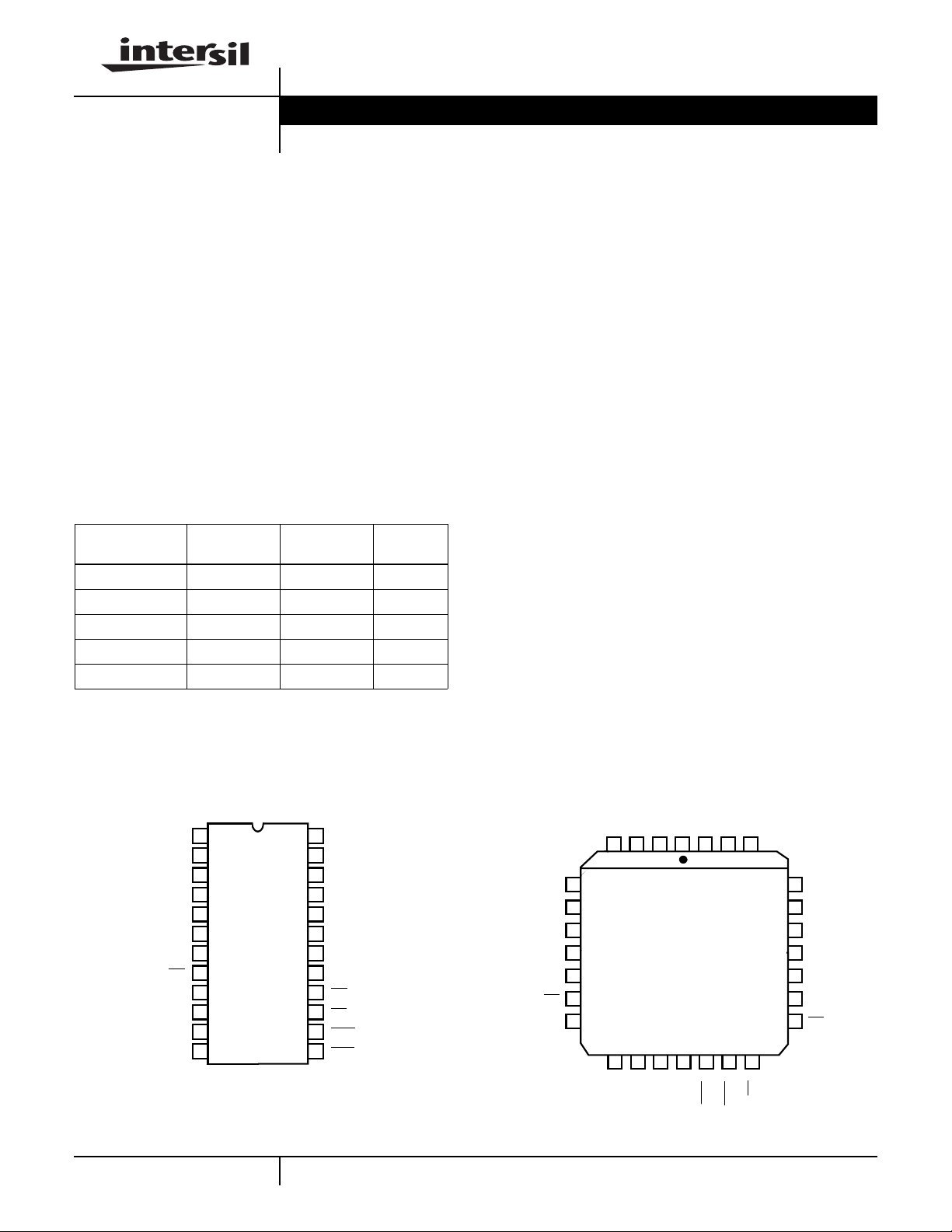
Pinouts
(PDIP, CERDIP, SOIC)
1
TIP
2
RING
+
V
3
B
4
C1*
5
C3
6
DG
7
RS
8
RD
9
TF
10
RF
V
-
11
B
12
BG
HC-5502B
TOP VIEW
47
HC-5502B
(PLCC)
TOP VIEW
B
RING
TIP
TX
AG
SHD
17 18
GKD
C4
262728
PD
RX
25
+IN
24
23
-IN
22
N/C
OUT
21
C2
20
RC
19
† OPTIONAL
24
TX
23
AG
22
C4
21
R
X
20
+IN
19
-IN
18
OUT
17
C2
16
RC
15
PD
14
GKD
13
SHD
CAUTION: These devices are sensitive to electrostatic discharge; follow proper IC Handling Procedures.
http://www.intersil.com or 407-727-9207 | Copyright © Intersil Corporation 1999
C1†
C3
DG
N/C
RS
RD
TF
10
11
V+
4
5
6
7
8
9
12
13 14
RF
N/C
23
1
15 16
-
B
BG
V
N/C

HC-5502B
Absolute Maximum Ratings (Note 1) Thermal Information
Supply Voltage
(VB-). . . . . . . . . . . . . . . . . . . . . . . . . . . . . . . . . . . . . . . -60 to 0.5V
(VB+) . . . . . . . . . . . . . . . . . . . . . . . . . . . . . . . . . . . . . . -0.5 to 15V
(VB+ - VB-) . . . . . . . . . . . . . . . . . . . . . . . . . . . . . . . . . . . . . . . .75V
Relay Drive Voltage (VRD). . . . . . . . . . . . . . . . . . . . . . . . -0.5 to 15V
Operating Conditions
Relay Driver Voltage (VRD) . . . . . . . . . . . . . . . . . . . . . . . . 5V to 12V
Positive Supply Voltage (VB+) . . . 4.75V to 5.25V or 10.8V to 13.2V
Negative Supply Voltage (VB-). . . . . . . . . . . . . . . . . . . .-42V to -58V
High Level Logic Input Voltage. . . . . . . . . . . . . . . . . . . . . . . . . . 2.4V
Low Level Logic Input Voltage . . . . . . . . . . . . . . . . . . . . . . . . . . 0.6V
Loop Resistance (RL) . . . . . . . . . . . . . . . . . . . . . . . . . 200 to 1200Ω
Operating Temperature Range
HC-5502B-5 . . . . . . . . . . . . . . . . . . . . . . . . . . . . . . . .0oC to 75oC
HC-5502B-9 . . . . . . . . . . . . . . . . . . . . . . . . . . . . . . -40oC to 85oC
CAUTION: Stresses above those listed in “Absolute Maximum Ratings” may cause permanent damage to the device. This is a stress only rating and operationofthe
device at these or any other conditions above those indicated in the operational sections of this specification is not implied.
NOTES:
1. Absolute maximum ratings are limiting values, applied individually, beyond which the serviceability of the circuit may be impaired.
Functional operability under any of these conditions is not necessarily implied.
2. θJA is measured with the component mounted on an evaluation PC board in free air.
Thermal Resistance (Typical, Note 2) θJA (oC/W)
CERDIP Package. . . . . . . . . . . . . . . . . . . . . . . . . . . 52
PDIP Package . . . . . . . . . . . . . . . . . . . . . . . . . . . . . 65
SOIC Package . . . . . . . . . . . . . . . . . . . . . . . . . . . . . 75
PLCC Package. . . . . . . . . . . . . . . . . . . . . . . . . . . . . 65
Maximum Junction Temperature (Hermetic Package). . . . . . .175oC
Maximum Junction Temperature (Plastic Package). . . . . . . . .150oC
Maximum Storage Temperature Range. . . . . . . . . . -65oC to 150oC
Maximum Lead Temperature (Soldering 10s) . . . . . . . . . . . . .300oC
(PLCC and SOIC - Lead Tips Only)
Die Characteristics
Transistor Count. . . . . . . . . . . . . . . . . . . . . . . . . . . . . . . . . . . . . .183
Diode Count. . . . . . . . . . . . . . . . . . . . . . . . . . . . . . . . . . . . . . . . . .33
Die Dimensions . . . . . . . . . . . . . . . . . . . . . . . . . .137 mils x 102 mils
Substrate Potential. . . . . . . . . . . . . . . . . . . . . . . . . . . . . . . . . . . . VB-
Process . . . . . . . . . . . . . . . . . . . . . . . . . . . . . . . . . . . . . . .Bipolar-DI
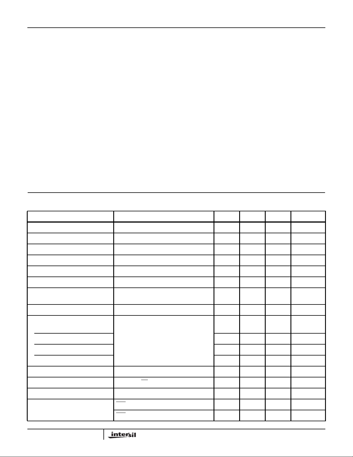
Electrical Specifications Unless Otherwise Specified, V
- = -48V, VB+ = 12V and 5V, AG = BG = DG = 0V, Typical Parameters
B
TA = 25oC. Min-Max Parameters are Over Operating Temperature Range
PARAMETER TEST CONDITIONS MIN TYP MAX UNITS
On Hook Power Dissipation I
Off Hook Power Dissipation RL = 600Ω, I
Off Hook IB+R
Off Hook IB+R
Off Hook IB-R
Off Hook Loop Current RL = 1200Ω, I
Off Hook Loop Current RL = 1200Ω, VB- = -42V, I
= 0, VB+ = 12V (Note 3) - 135 235 mW
LONG
= 0, VB+ = 12V (Note 3) - 450 690 mW
LONG
= 600Ω, I
L
= 600Ω, I
L
= 600Ω, I
L
= 0, TA = -40oC (Note 3) - - 6.0 mA
LONG
= 0, TA = 25oC (Note 3) - - 5.3 mA
LONG
= 0 (Note 3) - - 39 mA
LONG
= 0 (Note 3) - 21 - mA
LONG
= 0, TA = 25oC
LONG
17.5 - - mA
(Note 3)
Off Hook Loop Current RL = 200Ω, I
= 0 (Note 3) 25.5 30 34.5 mA
LONG
Fault Currents
TIP to Ground -14- mA
RING to Ground -47- mA
TIP to RING -30- mA
TIP and RING to Ground - 47 - mA
Ring Relay Drive V
OL
IOL = 62mA - 0.2 0.5 V
Ring Relay Driver Off Leakage VRD = 12V, RC = 1 = HIGH, TA = 25oC - - 100 µA
Ring Trip Detection Period RL = 600Ω, TA = 25oC - 2 3 Ring Cycles
Switch Hook Detection Threshold SHD = V
SHD = V
OL
OH
10 - - mA
--5 mA
48

HC-5502B
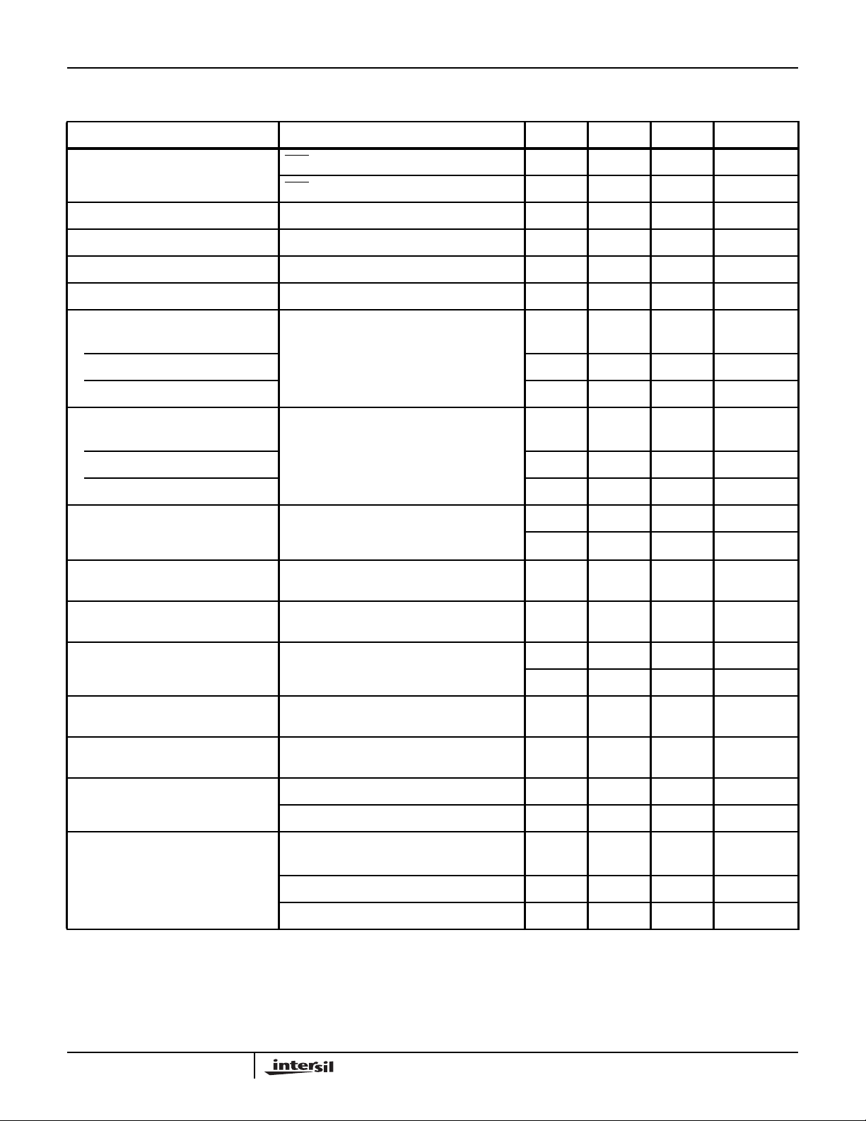
Electrical Specifications Unless Otherwise Specified, V
TA = 25oC. Min-Max Parameters are Over Operating Temperature Range (Continued)
PARAMETER TEST CONDITIONS MIN TYP MAX UNITS
Ground Key Detection Threshold GKD = V
GKD = V
Loop Current During Power Denial RL = 200Ω - ±2- mA
Dial Pulse Distortion 0-5 ms
Receive Input Impedance (Note 4) - 110 - kΩ
Transmit Output Impedance (Note 4) - 10 20 Ω
2-Wire Return Loss Referenced to 600Ω +2.16µF (Note 4)
SRL LO - 15.5 - dB
ERL -24- dB
SRL HI -31- dB
Longitudinal Balance 1V
2-Wire Off Hook IEEE Method
0oC ≤ TA≤ 75oC
2-Wire On Hook 60 63 - dB
4-Wire Off Hook 50 58 - dB
OL
OH
200Hz - 3400Hz, (Note 4)
RMS
- = -48V, VB+ = 12V and 5V, AG = BG = DG = 0V, Typical Parameters
B
20 - - mA
- - 10 mA
58 65 - dB
Low Frequency Longitudinal Balance R.E.A. Method, (Note 4)
RL = 600Ω,
0oC ≤ TA≤ 75oC
Insertion Loss
2-Wire to 4-Wire, 4-Wire to 2-Wire
Frequency Response 200 - 3400Hz Referenced to Absolute
Idle Channel Noise
2-Wire to 4-Wire, 4-Wire to 2-Wire
Absolute Delay
2-Wire to 4-Wire, 4-Wire to 2-Wire
Trans Hybrid Loss Balance Network Set Up for 600Ω
Overload Level
2-Wire to 4-Wire, 4-Wire to 2-Wire
Level Linearity At 1kHz, (Note 4) Referenced to 0dBm Level
2-Wire to 4-Wire, 4-Wire to 2-Wire +3 to -40dBm - - ±0.05 dB
At 1kHz, 0dBm Input Level, Referenced 600Ω - ±0.05 ±0.2 dB
Loss at 1kHz and 0dBm Signal Level (Note 4)
(Note 4) - 1 5 dBrnC
(Note 4) - - 2 µs
Termination at 1kHz
VB+ = 5V 1.5 V
VB+ = 12V 1.75 - - V
-40 to -50dBm - - ±0.1 dB
-50 to -55dBm - - ±0.3 dB
- - 23 dBrnC
- - -67 dBm0p
- ±0.02 ±0.05 dB
- -89 -85 dBm0p
36 40 - dB
PEAK
PEAK
49
 Loading...