Intersil Corporation HA-5340 Datasheet

HA-5340
Data Sheet September 1998 File Number 2859.3
700ns, Low Distortion, Precision Sample
and Hold Amplifier
The HA-5340 combines the advantages of two sample/ hold
architectures to create a new generation of monolithic
sample/hold. High amplitude, high frequency signals can be
sampled with very low distortion being introduced. The
combination of exceptionally fast acquisition time and
specified/characterized hold mode distortion is an industry
first. Additionally, the AC performance is only minimally
affected by additional hold capacitance.
To achieve this level of performance, the benefits of an
integrating output stage have been combined with the
advantages of a buff ered hold capacitor. To the user this
translates to a front-endstagethat has high bandwidth due to
charging only a small capacitive load and an output stage with
constant pedestal error which can be nulled out using the
offset adjust pins. Since the performance penalty for
additional hold capacitance is low , the designer can further
minimize pedestal error and droop rate without sacrificing
speed.
Low distortion, fast acquisition, and low droop rate are the
result, making the HA-5340 the obvious choice for high
speed, high accuracy sampling systems. For a Military
temperature range version request the HA-5340/883 data
sheet.
Ordering Information
TEMP.
PART NUMBER
RANGE (oC) PACKAGE
HA3-5340-5 0 to 75 14 Ld PDIP E14.3
HA9P5340-5 0 to 75 16 Ld SOIC M16.3
PKG.
NO.
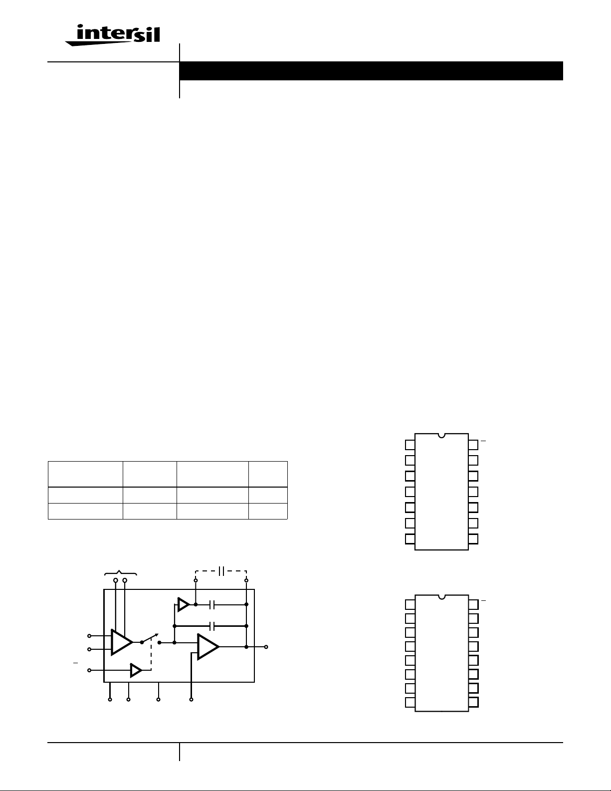
Functional Diagram
C
HOLD EXTERNAL
(OPTIONAL)
11
6
SIGNAL GND
C
HOLD
120pF
C
COMP
15pF
7
OUT
-IN
+IN
S/H
CONTROL
ADJUST OFFSET
437
1
2
14
95 13
V+
SUPPLYV-
GND
Features
• Fast Acquisition Time (0.01%) . . . . . . . . . . . . . . . . .700ns
• Fast Hold Mode Settling Time (0.01%). . . . . . . . . . . .200n
• Low Distortion (Hold Mode) . . . . . . . . . . . . . . . . . . -72dBc
(VIN = 200kHz, fS = 450kHz, 5V
• Bandwidth Minimally Affected By External C
P-P
)
H
• Fully Differential Analog Inputs
• Built-In 135pF Hold Capacitor
• Pin Compatible with HA-5320
Applications
• High Bandwidth Precision Data Acquisition Systems
• Inertial Navigation and Guidance Systems
• Ultrasonics
• SONAR
• RADAR
Pinouts
HA-5340
(PDIP)
TOP VIEW
-IN
+IN
OFFSET ADJ.
OFFSET ADJ.
SIG. GND
OUTPUT
-IN
+IN
OFFSET ADJ.
OFFSET ADJ.
NC
SIG. GND
OUTPUT
V-
V-
1
2
3
4
5
6
7
HA-5340
(SOIC)
TOP VIEW
1
2
3
4
5
6
7
8
S/H CONTROL
14
13
SUPPLY GND
12
NC
EXTERNAL
11
HOLD CAP.
10
NC
9
V+
8
NC
16
S/H CONTROL
SUPPLY GND
15
NC
14
NC
13
EXTERNAL
12
HOLD CAP.
NC
11
NC
10
V+
9
1
CAUTION: These devices are sensitive to electrostatic discharge; follow proper IC Handling Procedures.
1-888-INTERSIL or 321-724-7143
| Copyright © Intersil Corporation 1999

HA-5340
Absolute Maximum Ratings Thermal Information
Voltage Between V+ and V- Terminals. . . . . . . . . . . . . . . . . . . . 36V
Differential Input Voltage . . . . . . . . . . . . . . . . . . . . . . . . . . . . . . 24V
Digital Input Voltage. . . . . . . . . . . . . . . . . . . . . . . . . . . . . . +8V, -6V
Output Current, Continuous. . . . . . . . . . . . . . . . . . . . . . . . . . ±20mA
Operating Conditions
Temperature Range
HA-5340-5 . . . . . . . . . . . . . . . . . . . . . . . . . . . . . . . . 0oC to 75oC
Supply Voltage Range (Typical). . . . . . . . . . . . . . . . . ±12V to ±18V
CAUTION: Stresses above those listed in “Absolute Maximum Ratings” may cause permanent damage to the device. This is a stress only rating and operation of the
device at these or any other conditions above those indicated in the operational sections of this specification is not implied.
NOTES:
1. Maximum power dissipation must be designed to maintain the junction temperature below 150oC for the plastic packages.
2. θJA is measured with the component mounted on an evaluation PC board in free air.
Thermal Resistance (Typical, Note 2) θJA (oC/W) θJC (oC/W)
PDIP Package . . . . . . . . . . . . . . . . . . . 90 N/A
SOIC Package . . . . . . . . . . . . . . . . . . . 95 N/A
Maximum Junction Temperature (Plastic Package, Note 1) . .150oC
Maximum Storage Temperature Range. . . . . . . . . . -65oC to 150oC
Maximum Lead Temperature (Soldering 10s) . . . . . . . . . . . . 300oC
(SOIC - Lead Tips Only)
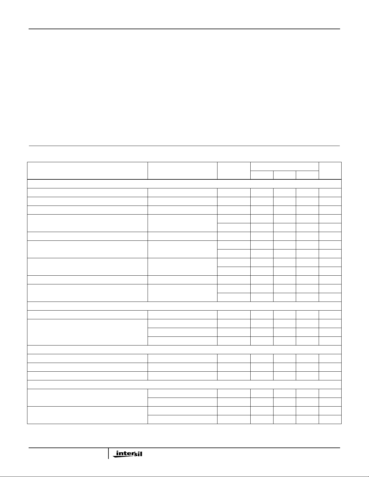
Electrical Specifications V
Gain Configuration (Output tied to -Input), R
PARAMETER TEST CONDITIONS TEMP. (
INPUT CHARACTERISTICS
Input Voltage Range Full -10 - +10 V
Input Resistance (Note 3) 25 - 1 - MΩ
Input Capacitance 25 - - 3 pF
Input Offset Voltage 25 - - 1.5 mV
Offset Voltage Temperature Coefficient Full - - 30 µV/oC
Bias Current 25 - ±70 - nA
Offset Current 25 - ±50 - nA
Common Mode Range Full -10 - +10 V
CMRR ±10V, Note 4 25 - 83 - dB
TRANSFER CHARACTERISTICS
Gain DC 25 110 140 - dB
Gain Bandwidth Product CH External = 0pF Full - 10 - MHz
TRANSIENT RESPONSE
Rise Time 200mV Step 25 - 20 30 ns
Overshoot 200mV Step 25 - 35 50 %
Slew Rate 10V Step 25 40 60 - V/µs
DIGITAL INPUT CHARACTERISTICS
Input Voltage V
Input Current VIL = 0V Full - 7 40 µA
= ±15.0V; CH = Internal = 135pF; Digital Input: VIL = +0.8V (Sample), VIH = +2.0V (Hold). Non-Inverting Unity
SUPPLY
CH External = 100pF Full - 9.6 - MHz
CH External = 1000pF Full - 6.7 - MHz
IH
V
IL
VIH = 5V Full - 4 40 µA
= 2kΩ, CL = 60pF, Unless Otherwise Specified
L
o
C)
Full - - 3.0 mV
Full - - ±350 nA
Full - - ±350 nA
Full 72 - - dB
Full 2.0 - - V
Full - - 0.8 V
HA-5340-5
UNITSMIN TYP MAX
2

HA-5340
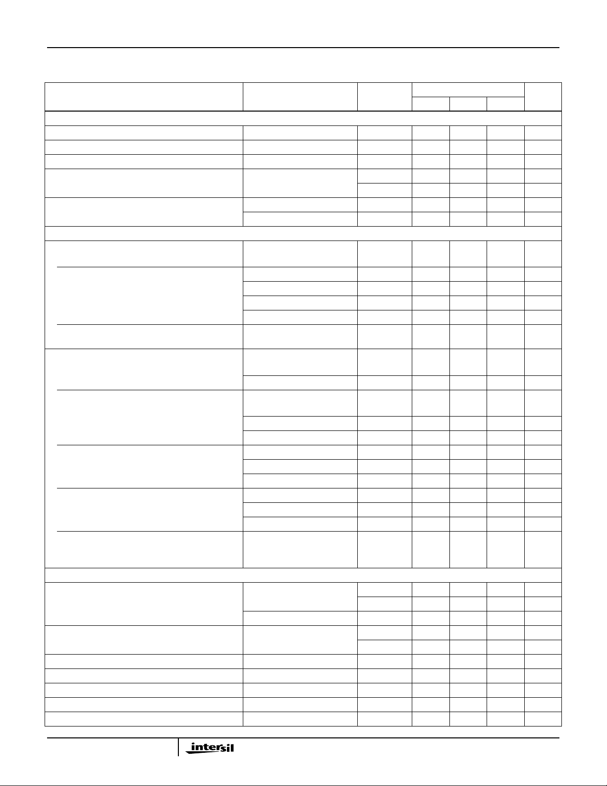
Electrical Specifications V
= ±15.0V; CH = Internal = 135pF; Digital Input: VIL = +0.8V (Sample), VIH = +2.0V (Hold). Non-Inverting Unity
SUPPLY
Gain Configuration (Output tied to -Input), RL = 2kΩ, CL = 60pF, Unless Otherwise Specified (Continued)
HA-5340-5
PARAMETER TEST CONDITIONS TEMP. (
o
C)
UNITSMIN TYP MAX
OUTPUT CHARACTERISTICS
Output Voltage Full -10 - +10 V
Output Current Full -10 - +10 mA
Full Power Bandwidth (Note 5) Full 0.6 0.9 - MHz
Output Resistance Hold Mode 25 - 0.05 0.1 Ω
Full - 0.07 0.15 Ω
Total Output Noise
DC to 10MHz
Sample Mode 25 - 325 400 µV
Hold Mode 25 - 325 400 µV
DISTORTION CHARACTERISTICS
SAMPLE MODE
Signal to Noise Ratio (RMS Signal to RMS Noise) V
= 200kHz, 20V
IN
Total Harmonic Distortion VIN = 200kHz, 5V
VIN = 200kHz, 10V
VIN = 200kHz, 20V
VIN = 500kHz, 5V
Intermodulation Distortion VIN = 10V
, f1 = 20kHz,
P-P
P-P
P-P
P-P
P-P
P-P
Full - 115 - dB
Full -90 -100 - dBc
Full -76 -82 - dBc
Full -70 -74 - dBc
Full -66 -75 - dBc
Full -78 -83 - dBc
f2 = 21kHz
HOLD MODE (50% Duty Cycle S/H)
Signal to Noise Ratio
(RMS Signal to RMS Noise) f
= 450kHz
S
VIN = 200kHz, 5V
VIN = 200kHz, 10V
P-P
P-P
25 - 76 - dB
25 - 76 - dB
Total Harmonic Distortion
= 450kHz VIN = 200kHz, 5V
f
S
VIN = 200kHz, 10V
VIN = 200kHz, 20V
fS = 450kHz VIN = 100kHz, 5V
VIN = 100kHz, 10V
VIN = 100kHz, 20V
fS = 2fIN(Nyquist) VIN = 20kHz, 5V
VIN = 50kHz, 5V
VIN = 100kHz, 5V
P-P
P-P
P-P
P-P
P-P
P-P
P-P
P-P
P-P
25 - -72 - dBc
25 - -66 - dBc
25 - -56 - dBc
25 - -84 - dBc
25 - -71 - dBc
25 - -61 - dBc
25 - -95 - dBc
25 - -91 - dBc
25 - -82 - dBc
Intermodulation Distortion
= 450kHz VIN = 10V
f
S
P-P
25 - -79 - dBc
(f1 = 20kHz, f2 = 21kHz)
SAMPLE AND HOLD CHARACTERISTICS
Acquisition Time 10V Step to 0.01% 25 - 700 - ns
Full - - 900 ns
10V Step to 0.1% 25 - 430 600 ns
Droop Rate CH = Internal 25 - 0.1 - µV/µs
Full - - 95 µV/µs
Hold Step Error VIL = 0V, VIH = 4.0V, tR = 5ns 25 - 15 - mV
Hold Mode Settling Time To ±1mV Full - 200 300 ns
Hold Mode Feedthrough 20V
, 200kHz, Sine Full - -76 - dB
P-P
EADT (Effective Aperture Delay Time) 25 - -15 - ns
Aperture Uncertainty 25 - 0.2 - ns
RMS
RMS
3
 Loading...