HA-5320
Data Sheet April 1999
1 Microsecond Precision Sample and
Hold Amplifier
The HA-5320 was designed for use in precision, high speed
data acquisition systems.
The circuit consists of an input transconductance amplifier
capable of providing large amounts of charging current, a low
leakage analog switch,and an output integrating amplifier.The
analog switch sees virtual ground as its load; therefore, charge
injection on the hold capacitor is constant over the entire
input/output voltage range. The pedestalvoltage resulting from
this charge injection can be adjusted to zerobyuse of the offset
adjust inputs. The device includes a hold capacitor . Ho w e v er, if
improved droop rate is required at the e xpense of acquisition
time, additional hold capacitance may be added e xternally.
This monolithic device is manufactured using the Intersil
Dielectric Isolation Process, minimizing stray capacitance
and eliminating SCRs. This allows higher speed and latchfree operation. For further information, please see
Application Note AN538.
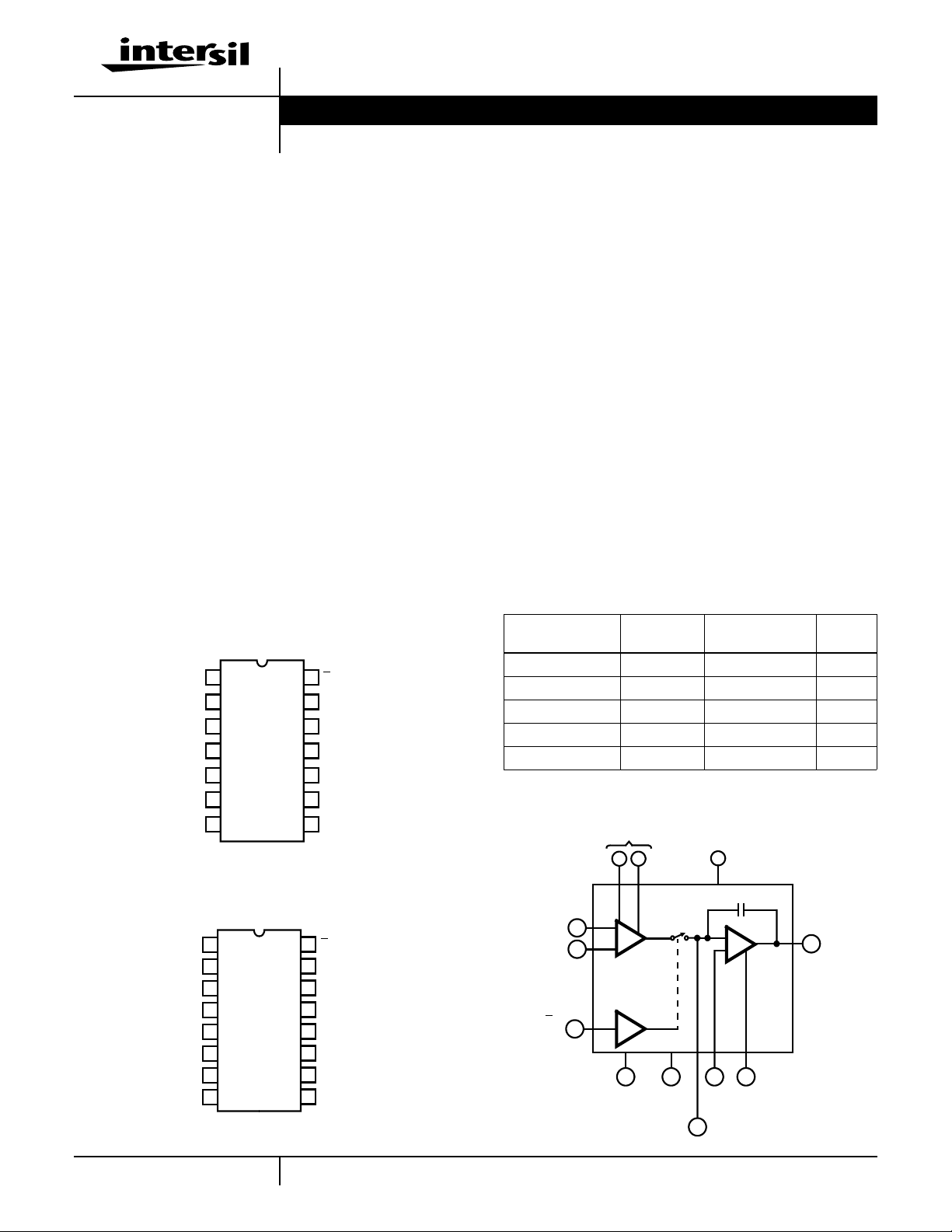
Pinouts
HA-5320
(PDIP, CERDIP)
TOP VIEW
-INPUT
+INPUT
OFFSET ADJUST
OFFSET ADJUST
SIG. GND
OUTPUT
-INPUT
+INPUT
OFFSET ADJUST
OFFSET ADJUST
SIG. GND
OUTPUT
NC
V-
V-
1
2
3
4
5
6
7
HA-5320
(SOIC)
TOP VIEW
1
2
3
4
5
6
7
8
S/H CONTROL
14
13
SUPPLY GND
12
NC
11
C
EXT
10
NC
9
V+
INTEGRATOR
8
BANDWIDTH
16
S/H CONTROL
SUPPLY GND
15
NC
14
C
13
EXT
NC
12
V+
11
INTEGRATOR
10
BANDWIDTH
NC
9
File Number 2857.4
Features
• Gain, DC. . . . . . . . . . . . . . . . . . . . . . . . . . . . . 2 x 10⁶ V/V
• Acquisition Time. . . . . . . . . . . . . . . . . . . . . 1.0µs (0.01%)
o
• Droop Rate. . . . . . . . . . . . . . . . . . . . . . 0.08µV/µs (25
C)
17µV/µs (Full Temperature)
• Aperture Time . . . . . . . . . . . . . . . . . . . . . . . . . . . . . 25ns
• Hold Step Error (See Glossary) . . . . . . . . . . . . . . . . . 5mV
• Internal Hold Capacitor
• Fully Differential Input
• TTL Compatible
Applications
• Precision Data Acquisition Systems
• Digital to Analog Converter Deglitcher
• Auto Zero Circuits
• Peak Detector
Ordering Information
TEMP.
PART NUMBER
RANGE (oC) PACKAGE
HA1-5320-2 -55 to 25 14 Ld CERDIP F14.3
HA1-5320-5 0 to 75 14 Ld CERDIP F14.3
HA3-5320-5 0 to 75 14 Ld PDIP E14.3
HA9P5320-5 0 to 75 16 Ld SOIC M16.3
HA9P5320-9 -40 to 85 16 Ld SOIC M16.3
PKG.
NO.
Functional Diagram
OFFSET
-INPUT
+INPUT
S/H
CONTROL
ADJUST
3 4
HA-5320
1
2
14
13
SUPPLY
GND
V+
9
100pF
-
+
5 6 8
V-
SIG.
GND
C
11
EXT
7
INTEGRATOR
BANDWIDTH
OUTPUT
1
CAUTION: These devices are sensitive to electrostatic discharge; follow proper IC Handling Procedures.
1-888-INTERSIL or 321-724-7143
| Copyright © Intersil Corporation 1999

HA-5320
Absolute Maximum Ratings Thermal Information
Supply Voltage. . . . . . . . . . . . . . . . . . . . . . . . . . . . . . . . . . . . . . .40V
Differential Input Voltage . . . . . . . . . . . . . . . . . . . . . . . . . . . . . . .24V
Digital Input Voltage. . . . . . . . . . . . . . . . . . . . . . . . . . . . . +8V, -15V
Output Current, Continuous (Note 1). . . . . . . . . . . . . . . . . . . ±20mA
Operating Conditions
Temperature Range
HA-5320-2 . . . . . . . . . . . . . . . . . . . . . . . . . . . . . . -55oC to 125oC
HA-5320-5 . . . . . . . . . . . . . . . . . . . . . . . . . . . . . . . . 0oC to 75oC
HA-5320-9 . . . . . . . . . . . . . . . . . . . . . . . . . . . . . . . -40oCto85oC
Supply Voltage Range (Typical, Note 2) . . . . . . . . . ±13.5V to ±20V
CAUTION: Stresses above those listed in “Absolute Maximum Ratings” may cause permanent damage to the device. This is a stress only rating and operation of the
device at these or any other conditions above those indicated in the operational sections of this specification is not implied.
NOTES:
1. Internal Power Dissipation may limit Output Current below 20mA.
2. Specification based on a one time characterization. This parameter is not guaranteed.
3. θJA is measured with the component mounted on an evaluation PC board in free air.
Thermal Resistance (Typical, Note 3) θJA (oC/W) θJC (oC/W)
CERDIP Package. . . . . . . . . . . . . . . . . 70 18
PDIP Package . . . . . . . . . . . . . . . . . . . 75 N/A
SOIC Package . . . . . . . . . . . . . . . . . . . 90 N/A
Maximum Junction Temperature (Ceramic Package) . . . . . . . . .175oC
Maximum Junction Temperature (Plastic Package) . . . . . . . .150oC
Maximum Storage Temperature Range. . . . . . . . . . -65oC to 150oC
Maximum Lead Temperature (Soldering 10s) . . . . . . . . . . . . 300oC
(SOIC - Lead Tips Only)
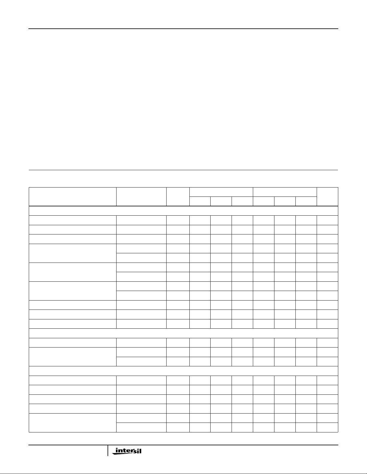
Electrical Specifications V
Unity Gain Configuration (Output tied to -Input), Unless Otherwise Specified
PARAMETER
INPUT CHARACTERISTICS
Input Voltage Range Full ±10 - - ±10 - - V
Input Resistance 25 1 5 - 1 5 - MΩ
Input Capacitance 25 - - 5 - - 5 pF
Offset Voltage 25 - 0.2 - - 0.5 - mV
Bias Current 25 - 70 200 - 100 300 nA
Offset Current 25 - 30 100 - 30 300 nA
Common Mode Range Full ±10 - - ±10 - - V
CMRR V
Offset Voltage Temperature Coefficient Full - 5 15 - 5 20 µV/
TRANSFER CHARACTERISTICS
Gain DC, (Note 12) 25 10
Gain Bandwidth Product
= +1, Note 5)
(A
V
OUTPUT CHARACTERISTICS
Output Voltage Full ±10 - - ±10 - - V
Output Current 25 ±10 - - ±10 - - mA
Full Power Bandwidth Note 4 25 - 600 - - 600 - kHz
Output Resistance Hold Mode 25 - 1.0 - - 1.0 - Ω
Total Output Noise (DC to 10MHz) Sample 25 - 125 200 - 125 200 µV
= ±5.0V; CH = Internal; Digital Input: VIL = +0.8V (Sample), VIH = +2.0V (Hold),
SUPPLY
TEST
CONDITIONS
= ±5V 25 80 90 - 72 90 - dB
CM
CH = 100pF 25 - 2.0 - - 2.0 - MHz
= 1000pF 25 - 0.18 - - 0.18 - MHz
C
H
Hold 25 - 125 200 - 125 200 µV
TEMP.
o
C)
(
Full - - 2.0 - - 1.5 mV
Full - - 200 - - 300 nA
Full - - 100 - - 300 nA
HA-5320-2/-9 HA-5320-5
6
2 x 10
6
- 3 x 1052 x 10
6
- V/V
UNITSMIN TYP MAX MIN TYP MAX
o
RMS
RMS
C
2

HA-5320
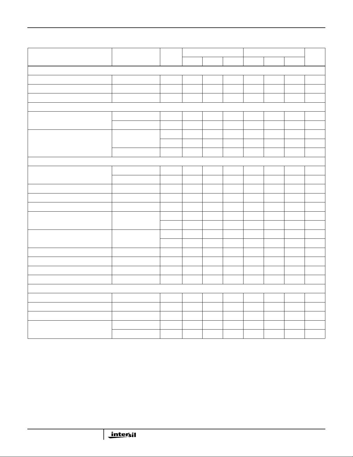
Electrical Specifications V
= ±5.0V; CH = Internal; Digital Input: VIL = +0.8V (Sample), VIH = +2.0V (Hold),
SUPPLY
Unity Gain Configuration (Output tied to -Input), Unless Otherwise Specified (Continued)
HA-5320-2/-9 HA-5320-5
UNITSMIN TYP MAX MIN TYP MAX
PARAMETER
TEST
CONDITIONS
TEMP.
o
(
C)
TRANSIENT RESPONSE
Rise Time Note 5 25 - 100 - - 100 - ns
Overshoot Note 5 25 - 15 - - 15 - %
Slew Rate Note 6 25 - 45 - - 45 - V/µs
DIGITAL INPUT CHARACTERISTICS
Input Voltage V
Input Current V
IH
V
IL
= 0V 25 - - 4 - - 4 µA
IL
Full 2.0 - - 2.0 - - V
Full - - 0.8 - - 0.8 V
Full - - 10 - - 10 µA
= +5V Full - - 0.1 - - 0.1 µA
V
IH
SAMPLE AND HOLD CHARACTERISTICS
Acquisition Time (Note 7) To 0.1% 25 - 0.8 1.2 - 0.8 1.2 µs
To 0.01% 25 - 1.0 1.5 - 1.0 1.5 µs
Aperture Time (Note 8) 25 - 25 - - 25 - ns
Effective Aperture Delay Time 25 -50 -25 0 -50 -25 0 ns
Aperture Uncertainty 25 - 0.3 - - 0.3 - ns
Droop Rate 25 - 0.08 0.5 - 0.08 0.5 µV/µs
Full - 17 100 - 1.2 100 µV/µs
Drift Current Note 9 25 - 8 50 - 8 50 pA
Full - 1.7 10 - 0.12 10 nA
Charge Transfer Note 9 25 - 0.5 1.1 - 0.5 1.1 pC
Hold Step Error Note 9 25 - 5 11 - 5 11 mV
Hold Mode Settling Time To 0.01% Full - 165 350 - 165 350 ns
Hold Mode Feedthrough 10V
, 100kHz Full - 2 - - 2 - mV
P-P
POWER SUPPLY CHARACTERISTICS
Positive Supply Current Note 10 25 - 11 13 - 11 13 mA
Negative Supply Current Note 10 25 - -11 -13 - -11 -13 mA
Supply Voltage Range Note 2 ±13.5 −±20 ±13.5 - ±20 V
Power Supply Rejection V+, Note 11 Full 80 - - 80 - - dB
V-, Note 11 Full 65 - - 65 - - dB
NOTES:
= 20V
4. V
O
5. VO = 200mV
; RL = 2kΩ; CL = 50pF; unattenuated output.
P-P
; RL = 2kΩ; CL = 50pF.
P-P
6. VO = 20V Step; RL = 2kΩ; CL = 50pF.
7. VO = 10V Step; RL = 2kΩ; CL = 50pF.
8. Derived from computer simulation only; not tested.
9. VIN = 0V, VIH = +3.5V, tR < 20ns (VIL to VIH).
10. Specified for a zero differential input voltage between +IN and -IN. Supply current will increase with differential input (as may occur in the Hold
mode) to approximately ±46mA at 20V.
11. Based on a 1V delta in each supply, i.e. 15V ±0.5VDC.
12. RL = 1kΩ, CL = 30pF.
3
 Loading...