Intersil Corporation HA-5222-883 Datasheet

January 1996
HA-5222/883
Dual, Low Noise, Wideband,
Precision Operational Amplifier
Features
• This Circuit is Processed in Accordance to MIL-STD883 and is Fully Conformant Under the Provisions of
Paragraph 1.2.1.
• Gain Bandwidth Product. . . . . . . . . . . . . 100MHz (Min)
• Unity Gain Bandwidth . . . . . . . . . . . . . . . . 30MHz (Min)
• High Slew Rate. . . . . . . . . . . . . . . . . . . . . . 25V/µs (Min)
• Low Offset Voltage. . . . . . . . . . . . . . . . . . 0.75mV (Max)
• High Open Loop Gain . . . . . . . . . . . . . . . . .106dB (Min)
• Channel Separation (at 10kHz). . . . . . . . . . 110dB (Typ)
• Low Voltage Noise (at 1kHz) . . . . . . . . 5.9nV/√
• Low Current Noise (at 1kHz). . . . . . . . 2.7pA/√
• High Output Current . . . . . . . . . . . . . . . . . ±30mA (Min)
• Low Supply Current (per Op Amp.) . . . . . . 10mA (Max)
40MHz (Typ)
37V/µs (Typ)
0.30mV (Typ)
128dB (Typ)
Hz (Max)
3.3nV/√
1.3pA/√
Hz (Typ)
Hz (Max)
Hz (Typ)
±56mA (Typ)
8mA (Typ)
Applications
• Precision Test Systems
• Active Filtering
• Small Signal Video
• Accurate Signal Processing
• RF Signal Conditioning
Description
The HA-5222/883 is a dual, high performance, dielectrically
isolated, monolithic op amp, featuring precision DC characteristics while providing excellent AC characteristics.
Designed for audio, video, and other demanding applications, noise (3.3nV/√
tion (<0.005% typ), and DC errors are kept to a minimum.
The precision performance is shown by low offset voltage
(0.3mV typ), low bias currents (40nA typ), low offset currents (15nA typ), and high open loop gain (128dB typ). The
combination of these excellent DC characteristics with fast
settling time (0.4µs typ) make the HA-5222/883 ideally
suited for precision signal conditioning.
The unique design of the HA-5222/883 gives this device outstanding AC characteristics, including high unity gain bandwidth (40MHz typ) and high slew rate (37V/µs typ), not
normally associated with precision op amps. Other key specifications include high CMRR (95dB typ) and high PSRR
(100dB typ). The combination of these specifications will
allow the HA-5222/883 to be used in RF signal conditioning
as well as video amplifiers.
Hz at 1kHz typ), total harmonic distor-
Ordering Information
PART
NUMBER
HA7-5222/883 -55oC to +125oC 8 Lead CerDIP
TEMPERATURE
RANGE PACKAGE
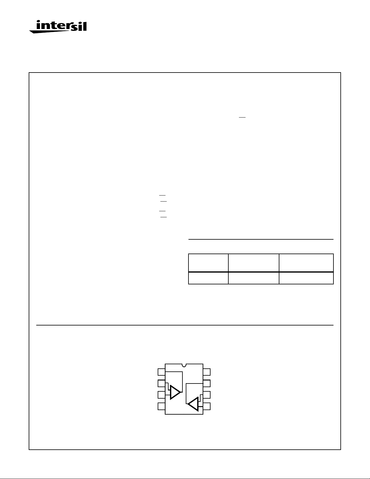
Pinout
HA-5222/883
(CERDIP)
TOP VIEW
1
OUT1
-IN1
2
1
-
+IN1
V-
CAUTION: These devices are sensitive to electrostatic discharge; follow proper IC Handling Procedures.
1-888-INTERSIL or 321-724-7143
| Copyright © Intersil Corporation 1999
+
3
4
3-169
8
V+
7
OUT2
6
2
-
+
-IN2
5
+IN2
Spec Number
File Number 3717.1
511062-883

Specifications HA-5222/883
Absolute Maximum Ratings Thermal Information (Typical)
Voltage Between V+ and V- Terminals . . . . . . . . . . . . . . . . . . . . 36V
Differential Input Voltage. . . . . . . . . . . . . . . . . . . . . . . . . . . . . . . . 5V
Voltage at Either Input Terminal . . . . . . . . . . . . . . . . . . . . . . V+ to V-
Peak Output Current (Pulsed at 1ms, 10% Duty Cycle). . . . .100mA
Continuous Output Current. . . . . . . . . . . . . . Short Circuit Protected
Junction Temperature. . . . . . . . . . . . . . . . . . . . . . . . . . . . . . +175oC
Storage Temperature Range . . . . . . . . . . . . . . . . . -65oC to +150oC
ESD Rating. . . . . . . . . . . . . . . . . . . . . . . . . . . . . . . . . . . . . . <2000V
Lead Temperature (Soldering 10s). . . . . . . . . . . . . . . . . . . . +300oC
CAUTION: Stresses above those listed in “Absolute Maximum Ratings” may cause permanent damage to the device. This is a stress only rating and operation
of the device at these or any other conditions above those indicated in the operational sections of this specification is not implied.
Operating Conditions
Operating Temperature Range. . . . . . . . . . . . . . . . -55oC to +125oC
Operating Supply Voltage . . . . . . . . . . . . . . . . . . . . . . . . . . ±5V to ±15V
TABLE 1. DC ELECTRICAL PERFORMANCE CHARACTERISTICS
Device Tested at: V
PARAMETERS SYMBOL CONDITIONS
Input Offset Voltage V
Input Bias Current +I
Input Offset Current I
Common Mode Range +CMR V+ = +3V, V- = -27V 1 +25oC12-V
Large Signal Voltage
Gain
Common Mode
Rejection Ratio
Output Voltage Swing +V
SUPPLY
= ±15V, R
= 1kΩ, V
LOAD
VCM = 0V 1 +25oC -0.75 0.75 mV
IO
VCM = 0V,
B
= 0V, Unless Otherwise Specified.
OUT
+RS = 100.1kΩ,
-RS = 100Ω
-I
VCM = 0V, +RS = 100Ω,
B
-RS = 100.1kΩ
IO
VCM = 0V,
+RS = 100.1kΩ,
-RS = 100.1kΩ
-CMR V+ = +27V, V- = -3V 1 +25oC - -12 V
+A
-A
VOL
VOL
V
= 0V and +10V 4 +25oC 106 - dB
OUT
V
= 0V and -10V 4 +25oC 106 - dB
OUT
+CMRR ∆VCM = +10V,
V+ = +5V, V- = -25V,
V
= -10V
OUT
-CMRR ∆VCM = -10V,
V+ = +25V, V- = -5V,
V
= +10V
OUT
OUT
-V
OUT
RL = 1kΩ 4 +25oC 12.0 - V
RL = 1kΩ 4 +25oC - -12.0 V
Thermal Resistance θ
JA
CerDIP Package . . . . . . . . . . . . . . . . . . . 96oC/W 16oC/W
Package Power Dissipation Limit at +75oC
CerDIP Package . . . . . . . . . . . . . . . . . . . . . . . . . . . . . . . . .1.04W
Package Power Dissipation Derating Factor Above +75oC
CerDIP Package . . . . . . . . . . . . . . . . . . . . . . . . . . . . .10.4mW/oC
V
≤ 1/2 (V+ - V-)
INCM
RL≥ 1kΩ
GROUP A
SUBGROUPS TEMPERATURE
LIMITS
UNITSMIN MAX
2, 3 +125oC, -55oC -1.5 1.5 mV
1 +25oC -80 80 nA
2, 3 +125oC, -55oC -200 200 nA
1 +25oC -80 80 nA
2, 3 +125oC, -55oC -200 200 nA
1 +25oC -50 50 nA
2, 3 +125oC, -55oC -150 150 nA
2, 3 +125oC, -55oC12 - V
2, 3 +125oC, -55oC - -12 V
5, 6 +125oC, -55oC 100 - dB
5, 6 +125oC, -55oC 100 - dB
1 +25oC88-dB
2, 3 +125oC, -55oC86 - dB
1 +25oC88-dB
2, 3 +125oC, -55oC86 - dB
5, 6 +125oC, -55oC 11.5 - V
5, 6 +125oC, -55oC - -11.5 V
θ
JC
3-170
Spec Number 511062-883

Specifications HA-5222/883
TABLE 1. DC ELECTRICAL PERFORMANCE CHARACTERISTICS (Continued)
Device Tested at: V
PARAMETERS SYMBOL CONDITIONS
Output Current +I
Quiescent Power Supply
Current
Power Supply
Rejection Ratio
SUPPLY
= ±15V, R
OUT
-I
OUT
+I
CC
-I
CC
+PSRR ∆V
-PSRR ∆V
= 1kΩ, V
LOAD
V
= +10V, RL = 1kΩ 4 +25oC30-mA
OUT
V
= -10V, RL = 1kΩ 4 +25oC - -30 mA
OUT
V
= 0V, I
OUT
V
= 0V, I
OUT
SUP
V+ = +20V, V- = -15V,
V+ = +10V, V- = -15V
SUP
V+ = +15V, V- = -20V,
V+ = +15V, V- = -10V
= 0V, Unless Otherwise Specified.
OUT
GROUP A
SUBGROUPS TEMPERATURE
= 0mA 1 +25oC - 20 mA
OUT
= 0mA 1 +25oC -20 - mA
OUT
= 10V,
= 10V,
LIMITS
UNITSMIN MAX
5, 6 +125oC, -55oC30 - mA
5, 6 +125oC, -55oC - -30 mA
2, 3 +125oC, -55oC - 22 mA
2, 3 +125oC, -55oC -22 - mA
1 +25oC90-dB
2, 3 +125oC, -55oC86 - dB
1 +25oC90-dB
2, 3 +125oC, -55oC86 - dB
TABLE 2. AC ELECTRICAL PERFORMANCE CHARACTERISTICS
Table 2 Intentionally Left Blank. See AC Specifications in Table 3.
TABLE 3. ELECTRICAL PERFORMANCE CHARACTERISTIC
Device Characterized at: V
SUPPLY
= ±15V, R
= 1kΩ, Unless Otherwise Specified.
LOAD
PARAMETERS SYMBOL CONDITIONS NOTES TEMPERATURE
Input Noise Voltage
E
RS = 0Ω, fO = 10Hz 1, 5 +25oC - 16.0 nV/√Hz
N
Density
RS = 0Ω, fO = 100Hz 1, 5 +25oC - 6.6 nV/√Hz
RS = 0Ω, fO = 1kHz 1, 5 +25oC - 5.9 nV/√Hz
Input Noise Current
I
RS = 500kΩ, fO = 10Hz 1, 5 +25oC - 24.0 pA/√Hz
N
Density
RS = 500kΩ, fO = 100Hz 1, 5 +25oC - 6.6 pA/√Hz
RS = 500kΩ, fO = 1kHz 1, 5 +25oC - 2.7 pA/√Hz
Gain Bandwidth Product GBWP V
OUT
= 200mV
P-P
,
1 +25oC 100 - MHz
fO = 100kHz
-55oC to +125oC 88 - MHz
LIMITS
UNITSMIN MAX
Unity Gain Bandwidth UGBW V
Slew Rate ±SR V
Full Power Bandwidth FPBW V
= 200mV 1 +25oC 30 - MHz
OUT
-55oC to +125oC 25 - MHz
OUT
= ±2.5V,
1 -55oC to +125oC25 - V/µs
CL = 50pF
= 10V 1, 2 -55oC to +125oC 398 - kHz
PEAK
Spec Number
3-171
511062-883
 Loading...