

Intersil Corporation HA-5221 Datasheet
TM
HA-5221
Data Sheet April 2000
100MHz, Low Noise, Precision
Operational Amplifier
The HA-5221 is a single high performance dielectrically
isolated, op amp, featuring precision DC characteristics while
providing excellent A C char acteristics. Designed for audio,
video,and other demanding applications, noise (3.4nV/√
1kHz), total harmonic distortion (<0.005%), and DC errors are
kept to a minimum.
The precision performance is shown by low offset voltage
(0.3mV), low bias currents (40nA), low offset currents
(15nA), and high open loop gain (128dB). The combination
of these excellent DC characteristics with the fast settling
time (0.4µs) makes the HA-5221 ideally suited for precision
signal conditioning.
The unique design of the HA-5221 gives it outstanding AC
characteristics not normally associated with precision op
amps, high unity gain bandwidth (35MHz) and high slew rate
(25V/µs). Other key specifications include high CMRR (95dB)
and high PSRR (100dB). The combination of these
specifications will allow the HA-5221 to be used in RF signal
conditioning as well as video amplifiers.
For MIL-STD-883C compliant product and Ceramic LCC
packaging, consult the HA-5221/883C data sheet. (Intersil
AnswerFAX (321-724-7800) Document #3716.)
Hz at
File Number 2915.5
Features
• Gain Bandwidth Product. . . . . . . . . . . . . . . . . . . . 100MHz
• Unity Gain Bandwidth. . . . . . . . . . . . . . . . . . . . . . . 35MHz
• Slew Rate. . . . . . . . . . . . . . . . . . . . . . . . . . . . . . . . 25V/µs
• Low Offset Voltage . . . . . . . . . . . . . . . . . . . . . . . . . 0.3mV
• High Open Loop Gain. . . . . . . . . . . . . . . . . . . . . . . 128dB
• Low Noise Voltage at 1kHz. . . . . . . . . . . . . . . . 3.4nV/√
Hz
• High Output Current. . . . . . . . . . . . . . . . . . . . . . . . . 56mA
• Low Supply Current . . . . . . . . . . . . . . . . . . . . . . . . . . 8mA
Applications
• Precision Test Systems
• Active Filtering
• Small Signal Video
• Accurate Signal Processing
• RF Signal Conditioning
Pinout
HA-5221
(CERDIP, SOIC)
TOP VIEW
Ordering Information
PART NUMBER
(BRAND)
HA7-5221-5 0 to 75 8 Ld CERDIP F8.3A
HA9P5221-5
(H52215)
TEMP.
RANGE (oC) PACKAGE
0 to 75 8 Ld SOIC M8.15
PKG.
NO.
-BAL
-IN
+IN
V-
1
2
+
3
4
8
7
6
5
+BAL
V+
OUT
NC
1
1-888-INTERSIL or 321-724-7143 | Intersil and Design is a trademark of Intersil Corporation. | Copyright © Intersil Corporation 2000
CAUTION: These devices are sensitive to electrostatic discharge; follow proper IC Handling Procedures.
HA-5221
Absolute Maximum Ratings Thermal Information
Supply Voltage Between V+ and V- Terminals. . . . . . . . . . . . . . 35V
Differential Input Voltage (Note 1) . . . . . . . . . . . . . . . . . . . . . . . . 5V
Output Current Short Circuit Duration . . . . . . . . . . . . . . . . Indefinite
Operating Conditions
Temperature Range
HA-5221-5 . . . . . . . . . . . . . . . . . . . . . . . . . . . . . . . . 0oC to 75oC
CAUTION: Stresses above those listed in “Absolute Maximum Ratings” may cause permanent damage to the device. This is a stress only rating and operation of the
device at these or any other conditions above those indicated in the operational sections of this specification is not implied.
NOTES:
1. Input is protected by back-to-back zener diodes. See applications section.
2. θJA is measured with the component mounted on an evaluation PC board in free air.
Thermal Resistance (Typical, Note 2) θJA (oC/W) θJC (oC/W)
CERDIP Package. . . . . . . . . . . . . . . . . 135 50
SOIC Package . . . . . . . . . . . . . . . . . . . 157 N/A
Maximum Junction Temperature (Hermetic Package) . . . . . . . 175oC
Maximum Junction Temperature (Plastic Package) . . . . . . . 150oC
Maximum Storage Temperature Range. . . . . . . . . . -65oC to 150oC
Maximum Lead Temperature (Soldering 10s) . . . . . . . . . . . . 300oC
(SOIC - Lead Tips Only)
Electrical Specifications V
PARAMETER TEST CONDITIONS TEMP. (oC) MIN TYP MAX UNITS
INPUT CHARACTERISTICS
Input Offset Voltage 25 - 0.30 0.75 mV
Average Offset Voltage Drift Full - 0.5 - µV/oC
Input Bias Current 25 - 40 100 nA
Input Offset Current 25 - 15 100 nA
Input Offset Voltage Match 25 - 400 750 µV
Common Mode Range 25 ±12 - - V
Differential Input Resistance 25 - 70 - kΩ
Input Noise Voltage f = 0.1Hz to 10Hz 25 - 0.25 - µV
Input Noise Voltage Density (Notes 3, 11) f = 10Hz 25 - 6.2 10 nV/√Hz
= ±15V, Unless Otherwise Specified
SUPPLY
Full - 0.35 1.5 mV
Full - 70 200 nA
Full - 30 150 nA
Full - - 1500 µV
f = 100Hz 25 - 3.6 6 nV/√Hz
P-P
f = 1000Hz 25 - 3.4 4.0 nV/√Hz
Input Noise Current Density (Notes 3, 11) f = 10Hz 25 - 4.7 8.0 pA/√Hz
f = 100Hz 25 - 1.8 2.8 pA/√Hz
f = 1000Hz 25 - 0.97 1.8 pA/√Hz
THD+N Note 4 25 - <0.005 - %
TRANSFER CHARACTERISTICS
Large Signal Voltage Gain Note 5 25 106 128 - dB
Full 100 120 - dB
CMRR VCM = ±10V Full 86 95 - dB
Unity Gain Bandwidth -3dB 25 - 35 - MHz
2
HA-5221
Electrical Specifications V
= ±15V, Unless Otherwise Specified (Continued)
SUPPLY
PARAMETER TEST CONDITIONS TEMP. (oC) MIN TYP MAX UNITS
Gain Bandwidth Product 1kHz to 400kHz 25 - 100 - MHz
Minimum Stable Gain Full 1 - - V/V
OUTPUT CHARACTERISTICS
Output Voltage Swing RL = 333Ω Full ±10 - - V
RL = 1kΩ 25 ±12 ±12.5 - V
RL = 1kΩ Full ±11.5 ±12.1 - V
Output Current V
= ±10V Full ±30 ±56 - mA
OUT
Output Resistance 25 - 10 - Ω
Full Power Bandwidth Note 6 25 239 398 - kHz
TRANSIENT RESPONSE (Note 11)
Slew Rate Notes 7, 11 Full 15 25 - V/µs
Rise Time Notes 8, 11 Full - 13 20 ns
Overshoot Notes 8, 11 Full - 28 50 %
Settling Time (Notes 9, 10) 0.1% 25 - 0.4 - µs
0.01% 25 - 1.5 - µs
POWER SUPPLY
PSRR VS = ±10V to ±20V Full 86 100 - dB
Supply Current Full - 8 11 mA
NOTES:
3. Refer to typical performance curve in data sheet.
4. A
= 10, fO = 1kHz, VO = 5V
VCL
5. V
= 0 to ±10V, RL = 1kΩ, CL = 50pF.
OUT
6. Full Power Bandwidth is calculated by: FPBW = .
7. V
8. V
= ±2.5V, RL = 1kΩ, CL = 50pF.
OUT
= ±100mV, RL = 1kΩ, CL = 50pF.
OUT
, RL = 600Ω, 10Hz to 100kHz, minimum resolution of test equipment is 0.005%.
RMS
Slew Rate
-------------------------- -
2πV
PEAK
V
PEAK
10V=,
9. Settling time is specified for a 10V step and AV = -1.
10. See Test Circuits.
11. Guaranteed by characterization.
Test Circuits and Waveforms
V
IN
+
-
1kΩ
50pF
V
OUT
FIGURE 1. TRANSIENT RESPONSE TEST CIRCUIT
3
Test Circuits and Waveforms (Continued)
HA-5221
2.5V
0V
-2.5V
2.5V
0V
-2.5V
100mV
0V
V
IN
-100mV
100mV
0V
V
OUT
-100mV
V
= ±100mV
V
= 2.5V
OUT
Vertical Scale = 2V/Div.,
Horizontal Scale = 200ns/Div.
OUT
Vertical Scale = 100mV/Div.,
Horizontal Scale = 200ns/Div.
FIGURE 2. LARGE SIGNAL RESPONSE FIGURE 3. SMALL SIGNAL RESPONSE
V
SETTLE
5K
V
IN
2K
5K
2K
V
+
OUT
NOTES:
12. AV= -1.
13. Feedback and summing resistors must be matched (0.1%).
14. HP5082-2810 clipping diodes recommended.
15. Tektronix P6201 FET probe used at settling point.
FIGURE 4. SETTLING TIME TEST CIRCUIT
Application Information
Operation at Various Supply Voltages
The HA-5221 operates over a wide range of supply voltages
with little variation in performance. The supplies may be
varied from ±5V to ±15V.See typical performance curves for
variations in supply current, slew rate and output voltage
swing.
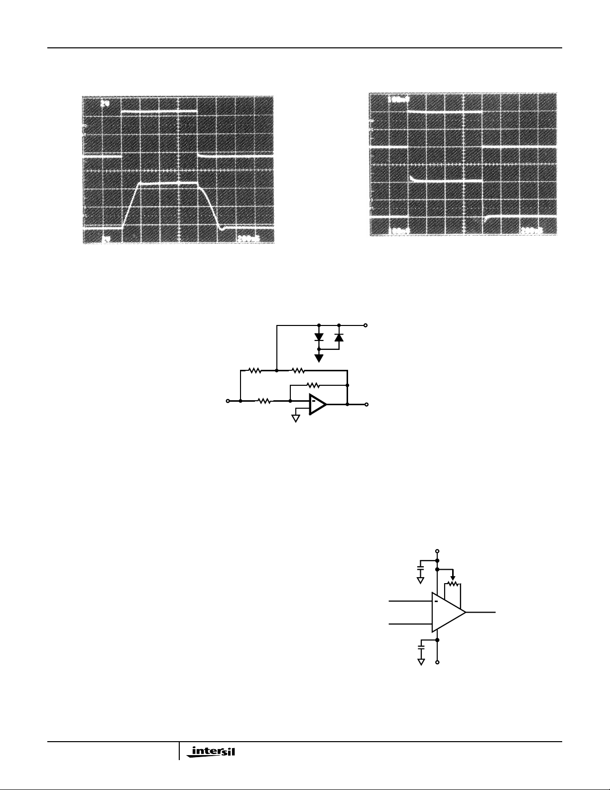
Offset Adjustment
The following diagram shows the offset voltage adjustment
configuration for the HA-5221. By moving the potentiometer
wiper towards pin 8 (+BAL), the op amps output voltage will
increase; towards pin 1 (-BAL) decreases the output voltage.
A 20kΩ trim pot will allow an offset voltage adjustment of
about 10mV.
+15V
7
R
2
3
P
1
8
6
+
4
-15V
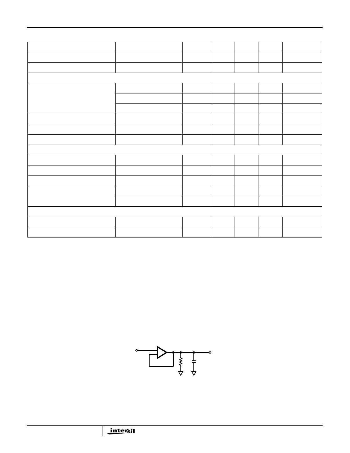
Capacitive Loading Considerations
When driving capacitive loads >80pF, a small resistor, 50Ω
to 100Ω, should be connected in series with the output and
inside the feedback loop.
4
 Loading...