

Page 1
®
http://www.BDTIC.com/Intersil
HA-5190, HA-5195
Data Sheet August 2002 FN2914.4
150MHz, Fast Settling Operational
Amplifiers
HA-5190/5195 are operational amplifiers featuring a
combination of speed, precision, and bandwidth. Employing
monolithic bipolar construction coupled with Dielectric
Isolation, these devices are capable of delivering 200V/µs
slew rate with a settling time of 70ns (0.1%, 5V output step).
These truly differential amplifiers are designed to operate at
gains ≥ 5 without the need for external compensation. Other
outstanding HA-5190/5195 features are 150MHz gain
bandwidth product and 6.5MHz full power bandwidth. In
addition to these dynamic characteristics, these amplifiers
also have excellent input characteristics such as 3mV offset
voltage and 6.0nV/√Hz
input voltage noise at 1kHz.
With 200V/µs slew rate and 70ns settling time, these devices
make ideal output amplifiers for accurate, high speed D/A
converters or the main components in high speed
sample/hold circuits. The 5190/5195 are also ideally suited
for a variety of pulse and wideband video amplifiers. Please
refer to Application Notes AN525 and AN526 for some of
these application designs.
At temperatures above 75
o
C a heat sink is required for the
HA-5190 (see Note 2 and Application Note AN556). For
military versions, please request the HA-5190/883 data sheet.
Ordering Information
TEMP.
PART NUMBER
HA1-5190-2 -55 to 125 14 Ld CERDIP F14.3
HA1-5195-5 0 to 75 14 Ld CERDIP F14.3
RANGE (oC) PACKAGE
PKG.
NO.
Features
• Fast Settling Time (0.1%). . . . . . . . . . . . . . . . . . . . . 70ns
• Very High Slew Rate . . . . . . . . . . . . . . . . . . . . . . 200V/µs
• Wide Gain-Bandwidth (A
≥ 5). . . . . . . . . . . . . . . 150MHz
V
• Full Power Bandwidth . . . . . . . . . . . . . . . . . . . . . 6.5MHz
• Low Offset Voltage . . . . . . . . . . . . . . . . . . . . . . . . . . . 3mV
• Input Noise Voltage . . . . . . . . . . . . . . . . . . . . . . 6nV/√Hz
• Bipolar D.I. Construction
Applications
• Fast, Precise D/A Converters
• High Speed Sample-Hold Circuits
• Pulse and Video Amplifiers
• Wideband Amplifiers
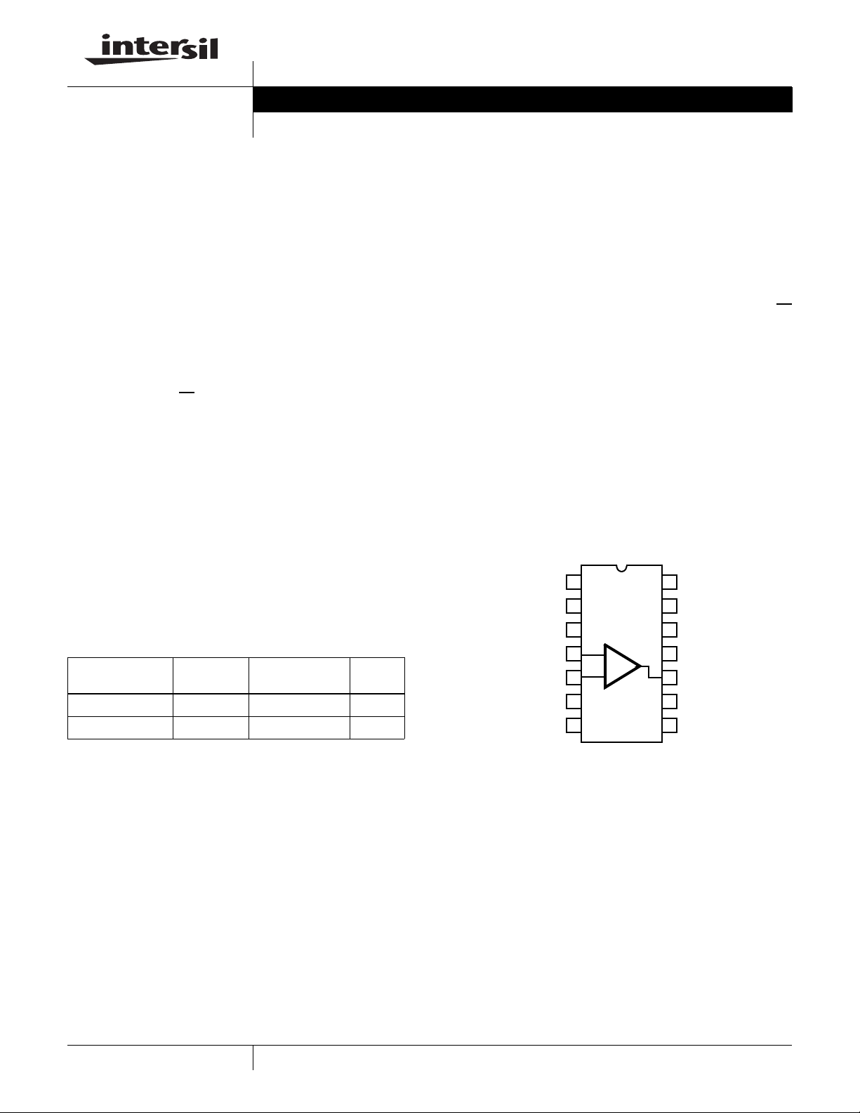
Pinout
HA-5190/95 (CERDIP)
TOP VIEW
NC
NC
NC
-IN
+IN
NC
1
2
3
4
-
+
5
6
V-
7
14
NC
13
NC
12
NC
11
V+
10
OUT
9
NC
8
NC
1
CAUTION: These devices are sensitive to electrostatic discharge; follow proper IC Handling Procedures.
1-888-INTERSIL or 321-724-7143
| Intersil (and design) is a trademark of Intersil Americas Inc.
Copyright © Intersil Americas Inc. 2002. All Rights Reserved
Page 2

HA-5190, HA-5195
http://www.BDTIC.com/Intersil
Absolute Maximum Ratings T
Supply Voltage (V+ to V-). . . . . . . . . . . . . . . . . . . . . . . . . . . . . . 35V
Differential Input Voltage . . . . . . . . . . . . . . . . . . . . . . . . . . . . . . . 6V
Output Current . . . . . . . . . . . . . . . . . . . . . . . . . . . . . . . 50mA (Peak)
Operating Conditions
Temperature Range
HA-5190-2 . . . . . . . . . . . . . . . . . . . . . . . . . . . . . . -55
HA-5195-5 . . . . . . . . . . . . . . . . . . . . . . . . . . . . . . . . 0
CAUTION: Stresses above those listed in “Absolute Maximum Ratings” may cause permanent damage to the device. This is a stress only rating and operation of the
device at these or any other conditions above those indicated in the operational sections of this specification is not implied.
NOTES:
1. Heat sinking may be required, especially at T
is measured with the component mounted on an evaluation PC board in free air.
2. θ
JA
Electrical Specifications V
PARAMETER
INPUT CHARACTERISTICS
Offset Voltage 25 - 3 5 - 3 6 mV
Average Offset Voltage Drift Full - 20 - - 20 - µV/
Bias Current 25 - 5 15 - 5 15 µA
Offset Current 25 - 1 4 - 1 4 µA
Input Resistance 25 - 10 - - 10 - kΩ
Input Capacitance 25 - 1 - - 1 - pF
Common Mode Range Full ±5- -±5- - V
Input Noise Current f = 1kHz, R
Input Noise Voltage f = 1kHz, RG = 0Ω 25 - 6 - - 6 - nV/√Hz
TRANSFER CHARACTERISTICS
Large Signal Voltage Gain (Note 3) 25 15 30 - 10 30 - kV/V
Common Mode Rejection Ratio ∆V
Minimum Stable Gain 25 5 - - 5 - - V/V
Gain-Bandwidth-Product V
OUTPUT CHARACTERISTICS
Output Voltage Swing (Note 3) Full ±5 ±8-±5 ±8- V
Output Current (Note 3) 25 ±25 ±30 - ±25 ±30 - mA
Output Resistance Open Loop 25 - 30 - - 30 - Ω
Full Power Bandwidth (Notes 3, 4) 25 5 6.5 - 5 6.5 - MHz
TRANSIENT RESPONSE (Note 5)
Rise Time 25 - 13 18 - 13 18 ns
Overshoot 25 - 8 - - 8 - %
Slew Rate 25 160 200 - 160 200 - V/µs
Settling Time (Note 5) 5V Step to 0.1% 25 70 - - 70 - - ns
=25oC Thermal Information
A
Thermal Resistance (Typical, Note 2) θ
CERDIP Package. . . . . . . . . . . . . . . . . . . 75 20
Maximum Junction Temperature (Hermetic Package, Note 1) . . 175
Maximum Storage Temperature Range. . . . . . . . . . -65
Maximum Lead Temperature (Soldering 10s) . . . . . . . . . . . . 300
o
C to 125oC
o
C to 75oC
≥ 75oC.
A
= ±15V, Unless Otherwise Specified
SUPPLY
TEST
CONDITIONS TEMP (
= 0Ω 25 - 5 - - 5 - pA/√Hz
G
= ±5V Full 74 95 - 74 95 - dB
CM
= 90mV, AV = 10 25 - 150 - 150 - - MHz
OUT
5V Step to 0.01% 25 - 100 - - 100 - ns
2.5V Step to 0.1% 25 - 50 - - 50 - ns
2.5V Step to 0.01% 25 - 80 - - 80 - ns
o
C)
Full - - 10 - - 10 mV
Full - - 20 - - 20 µA
Full - - 6 - - 6 µA
Full 5 - - 5 - - kV/V
HA-5190-2 HA-5195-5
(oC/W) θJC (oC/W)
JA
o
C to 150oC
UNITSMIN TYP MAX MIN TYP MAX
o
o
C
o
C
C
2
Page 3
HA-5190, HA-5195
http://www.BDTIC.com/Intersil
Electrical Specifications V
PARAMETER
= ±15V, Unless Otherwise Specified (Continued)
SUPPLY
TEST
CONDITIONS TEMP (
o
C)
HA-5190-2 HA-5195-5
UNITSMIN TYP MAX MIN TYP MAX
POWER SUPPLY CHARACTERISTICS
Supply Current Full - 19 28 - 19 28 mA
Power Supply Rejection Ratio ∆V
= ±10V to ±20V Full 70 90 - 70 90 - dB
S
NOTES:
3. R
= 200Ω, CL < 10pF, V
L
4. Full power bandwidth guaranteed based on slew rate measurement using: .
5. Refer to Test Circuits section of the data sheet.
OUT
= ±5V.
FPBW
Slew Rate
---------------------------- -=
2πV
PEAK
Test Circuits and Waveforms
IN
+
-
1.6kΩ
400Ω
FIGURE 1. LARGE AND SMALL SIGNAL RESPONSE TEST CIRCUIT
200Ω
OUT
NOTES:
6. A
V
7. C
L
= 5.
< 10pF.
V
-5V
V
-1V
SETTLE
OUT
IN
Vertical Scale: V
IN
POINT
+5V
90%
10%
+1V
= 2.0V/Div., V
IN
Horizontal Scale: 100ns/Div.
LARGE SIGNAL RESPONSE
400Ω
1kΩ
5kΩ
V
OUT
V
IN
OUT
= 4.0/Div.
Vertical Scale: VIN = 50mV/Div., V
= 100mV/Div.
OUT
Horizontal Scale: 100ns/Div
SMALL SIGNAL RESPONSE
0.001µF
V+
NOTES:
= -5.
8. A
1µF
-
+
0.001µF
OUT
PROBE
MONITOR
V
9. Load Capacitance should be less than 10pF.
10. It is recommended that resistors be carbon composition and that
feedback and summing network ratios be matched to 0.1%.
11. Settle Point (Summing Node) capacitance should be less than
V-
1µF
2kΩ
10pF. For optimum settling time results, it is recommended that
the test circuit be constructed directly onto the device pins. A
Tektronix 568 Sampling Oscilloscope with S-3A sampling heads
is recommended as a settle point monitor.
FIGURE 2. SETTLING TIME TEST CIRCUIT
3
Page 4

Schematic Diagram
http://www.BDTIC.com/Intersil
Q
P24
R
28
Q
P20
Q
P32
Q
Q
P44
P35
Q
N39
Q
N42
D
D
Q
P16
Q
N13
HA-5190, HA-5195
V+
R
1
R
6
R
7
Q
N21
Q
D
34
D
37
38
41
R
14
R
15
P33
Q
P36
Q
N40
Q
N43
R
10
R
11
Q
N17
R
2
Q
P23
Q
N14
R
16
Q
N56
Q
N22
R
8
R
9
Q
P19
+IN
Q
N18
R
Q
12
P55
R
13
Q
P15
Q
N1QN2
R24R
R
26
Q
P7
Q
N9
Q
N11
R
3
Q
P4
Q
P3
C
1C2
C
3
25
-IN
R
27
Q
P8
R
17
Q
Q
R
29
Q
N10QN45
Q
N12
R
4
P6
P5
Q
N49
Q
N50
Q
N53
D
51
D
52
Q
N47
R
R
18
30
R
32
OUT
R
33
Q
P54
Q
N46
Q
N48
R
31
V-
Application Information
Power Supply Decoupling
Although not absolutely necessary, it is recommended that
all power supply lines be decoupled with 0.01µF ceramic
capacitors to ground. Decoupling capacitors should be
located as near to the amplifier terminals as possible.
Stability Considerations
HA-5190/5195 is stable at gains > 5. Gains < 5 are covered
below. Feedback resistors should be of carbon composition
located as near to the input terminals as possible.
Wiring Considerations
Video pulse circuits should be built on a ground plane.
Minimum point to point connections directly to the amplifier
terminals should be used. When ground planes cannot be
used, good single point grounding techniques should be
applied.
4
Output Short Circuit
HA-5190/5195 does not have output short circuit protection.
Short circuits to ground can be tolerated for approximately
10 seconds. Short circuits to either supply will result in
immediate destruction of the device.
Heavy Capacitive Loads
When driving heavy capacitive loads (>100pF) a small
resistor (100Ω) should be connected in series with the output
and inside the feedback loop.
Page 5

HA-5190, HA-5195
http://www.BDTIC.com/Intersil
Typical Applications (Also see Application Notes AN525 and AN526)
IN
11pF
(NOTE)
OUTPUT
INPUT
+
C
1
-
R
750Ω (NOTE)
F
200Ω
Vertical Scale: 2V/Div.
Horizontal Scale: 100ns/Div
OUT
OUTPUT
.
INPUT
IN
1kΩ (NOTE)
+
-
R
1kΩ (NOTE)
Vertical Scale: 2V/Div.
Horizontal Scale: 100ns/Div
F
NOTE: Values were determined experimentally for optimum speed and settling time. RF and C1 should be optimized for each
particular application to ensure best overall frequency response.
FIGURE 3. SUGGESTED COMPENSATION FOR NONINVERTING UNITY GAIN AMPLIFIER
OUT
200Ω
1kΩ
1kΩ
IN
-
+
OUT
200Ω
OUTPUT
INPUT
Vertical Scale: 2V/Div.
Horizontal Scale: 50ns/Div
.
FIGURE 4. SUGGESTED COMPENSATION FOR INVERTING UNITY GAIN AMPLIFIER
V+
+
IN
-
200Ω
1.6kΩ
400Ω
120Ω
75Ω
50Ω
1µF1µF
+
HA-5190
-
1µF
200Ω
V-
HA-5033
1µF
50Ω
5kΩ
1kΩ
FIGURE 5. VIDEO PULSE AMPLIFIER/75Ω COAXIAL DRIVER FIGURE 6. VIDEO PULSE AMPLIFIER COAXIAL LINE DRIVER
5
Page 6

HA-5190, HA-5195
http://www.BDTIC.com/Intersil
Typical Performance Curves V
5
4
3
2
OFFSET VOLTAGE
1
INPUT BIAS CURRENT (µA)
0
0 40 80 160
TEMPERATURE (oC)
BIAS CURRENT
= ±15V, TA = 25oC, Unless Otherwise Specified
S
2.0
1.6
1.2
0.8
0.4
120-40-80
0
FIGURE 7. INPUT OFFSET VOLTAGE AND BIAS CURRENT vs
TEMPERATURE
18
)
16
P-P
14
12
10
8
6
OUTPUT VOLTAGE SWING (V
100
80
60
PHASE
20
OFFSET VOLTAGE (mV)
0
OPEN LOOP VOLTAGE GAIN (dB)
-20
10K1K
GAIN
100K
1M4010M
FREQUENCY (Hz)
100M
0
45
90
135
180
225
PHASE (DEGREES)
FIGURE 8. OPEN LOOP FREQUENCY RESPONSE
1.2
C
o
1.1
1.0
0.9
0.8
NORMALIZED PARAMETERS
0.7
REFERRED TO VALUES AT 25
BANDWIDTH
SLEW RATE
4
100K
FREQUENCY (Hz)
1M
10M
100M10K1K
04080 160
TEMPERATURE (oC)
FIGURE 9. OUTPUT VOLTAGE SWING vs FREQUENCY FIGURE 10. NORMALIZED AC PARAMETERS vs
TEMPERATURE
1.2
1.1
BANDWIDTH
1.0
SLEW RATE
0.9
NORMALIZED VALUE REFERRED TO
LOAD CAPACITANCE EQUAL TO 10pF
0.8
LOAD CAPACITANCE (pF)
20010010
FIGURE 11. NORMALIZED AC PARAMETERS vs LOAD
CAPACITANCE
250
1000
100
INPUT NOISE CURRENT
10
INPUT NOISE VOLTAGE
INPUT NOISE VOLTAGE (nV/√Hz)
1
1
FREQUENCY (Hz)
FIGURE 12. INPUT NOISE VOLTAGE AND NOISE CURRENT vs
FREQUENCY
120-40-80
1000
100
10
INPUT NOISE CURRENT (pA/√Hz)
1
100K10 10K1K100
6
Page 7

HA-5190, HA-5195
http://www.BDTIC.com/Intersil
Typical Performance Curves V
12
10
8
6
4
OUTPUT VOLTAGE SWING (V)
2
200 400 600 1.2K
LOAD RESISTANCE (Ω)
= ±15V, TA = 25oC, Unless Otherwise Specified (Continued)
S
5
2.5
0
-2.5
-5
OUTPUT VOLTAGE STEP (V)
8000
1K
10 40 60
5mV
5mV 0.5mV
30200
50
SETTLING TIME (ns)
0.5mV
70 80 90 100 110
FIGURE 13. OUTPUT VOLTAGE SWING vs LOAD RESISTANCE FIGURE 14. SETTLING TIME FOR VARIOUS OUTPUT STEP
VOLTAGES
120
100
80
120
100
80
POSITIVE
SUPPLY
60
40
20
COMMON MODE REJECTION RATIO (dB)
0
FREQUENCY (Hz)
100K
FIGURE 15. COMMON MODE REJECTION RATIO vs
FREQUENCY
24
20
16
12
8
4
POWER SUPPLY CURRENT (mA)
V
SUPPLY
V
SUPPLY
1M10K1K100
= ±15V
= ±10V
60
NEGATIVE
40
20
POWER SUPPLY REJECTION RATIO (dB)
0
SUPPLY
100K
FREQUENCY (Hz)
FIGURE 16. POWER SUPPLY REJECTION RATIO vs
FREQUENCY
1M10K1K100
0
0-80
40-40
TEMPERATURE (oC)
80
120
160
FIGURE 17. POWER SUPPLY CURRENT vs TEMPERATURE
7
Page 8

Die Characteristics
http://www.BDTIC.com/Intersil
DIE DIMENSIONS:
HA-5190, HA-5195
SUBSTRATE POTENTIAL (Powered Up):
54 mils x 88 mils x 19 mils
1360µm x 2240µm x 483µm
METALLIZATION:
Type: Al, 1% Cu
Thickness: 16k
PAS SIVATION:
Type: Nitride (Si3N4) over Silox (SiO2, 5% Phos.)
Silox Thickness: 12k
Nitride Thickness: 3.5kÅ ±1.5kÅ
Å ±2kÅ
Å ±2kÅ
Metallization Mask Layout
-IN V+
V-
TRANSISTOR COUNT:
49
PROCESS:
Bipolar Dielectric Isolation
HA-5190
OUTPUT
V-+IN
8
Page 9

HA-5190, HA-5195
http://www.BDTIC.com/Intersil
Ceramic Dual-In-Line Frit Seal Packages (CERDIP)
c1
LEAD FINISH
-A-
-B-
bbb C A - B
S
BASE
PLANE
SEATING
PLANE
S1
b2
b
ccc C A - BMD
D
A
A
e
S
S
NOTES:
1. Index area: A notch or a pin one identification mark shall be located adjacent to pin one and shall be located within the shaded
area shown. The manufacturer’s identification shall not be used
as a pin one identification mark.
2. The maximum limits of lead dimensions b and c or M shall be
measured at the centroid of the finished lead surfaces, when
solder dip or tin plate lead finish is applied.
3. Dimensions b1 and c1 apply to lead base metal only. Dimension
M applies to lead plating and finish thickness.
4. Corner leads (1, N, N/2, and N/2+1) may be configured with a
partial lead paddle. For this configuration dimension b3 replaces
dimension b2.
5. This dimension allows for off-center lid, meniscus, and glass
overrun.
6. Dimension Q shall be measured from the seating plane to the
base plane.
7. Measure dimension S1 at all four corners.
8. N is the maximum number of terminal positions.
9. Dimensioning and tolerancing per ANSI Y14.5M - 1982.
10. Controlling dimension: INCH.
-D-
BASE
E
D
S
S
Q
A
-C-
L
METAL
b1
M
(b)
SECTION A-A
α
(c)
M
eA
eA/2
aaa CA - B
M
c
D
S
S
F14.3 MIL-STD-1835 GDIP1-T14 (D-1, CONFIGURATION A)
14 LEAD CERAMIC DUAL-IN-LINE FRIT SEAL PACKAGE
INCHES MILLIMETERS
SYMBOL
A - 0.200 - 5.08 -
b 0.014 0.026 0.36 0.66 2
b1 0.014 0.023 0.36 0.58 3
b2 0.045 0.065 1.14 1.65 -
b3 0.023 0.045 0.58 1.14 4
c 0.008 0.018 0.20 0.46 2
c1 0.008 0.015 0.20 0.38 3
D - 0.785 - 19.94 5
E 0.220 0.310 5.59 7.87 5
e 0.100 BSC 2.54 BSC -
eA 0.300 BSC 7.62 BSC -
eA/2 0.150 BSC 3.81 BSC -
L 0.125 0.200 3.18 5.08 -
Q 0.015 0.060 0.38 1.52 6
S1 0.005 - 0.13 - 7
o
α
90
105
o
90
o
105
aaa - 0.015 - 0.38 -
bbb - 0.030 - 0.76 -
ccc - 0.010 - 0.25 -
M - 0.0015 - 0.038 2, 3
N14 148
NOTESMIN MAX MIN MAX
o
Rev. 0 4/94
-
All Intersil semiconductor products are manufactured, assembled and tested under ISO9000 quality systems certification.
Intersil semiconductor products are sold by description only. Intersil Corporation reserves the right to make changes in circuit design and/or specifications at any time without
notice. Accordingly, the reader is cautioned to verify that data sheets are current before placing orders. Information furnished by Intersil is believed to be accurate and reliable. However, no responsibility is assumed by Intersil or its subsidiaries for its use; nor for any infringements of patents or other rights of third parties which may result from
its use. No license is granted by implication or otherwise under any patent or patent rights of Intersil or its subsidiaries.
For information regarding Intersil Corporation and its products, see web site http://www.intersil.com
9
 Loading...