Intersil Corporation HA-5147-883 Datasheet

June 1998
HA-5147/883
100MHz, Ultra Low Noise, Precision,
High Slew Rate Operational Amplifier
Features
• This Circuit is Processed in Accordance to MIL-STD883 and is Fully Conformant Under the Provisions of
Paragraph 1.2.1.
• High Slew Rate. . . . . . . . . . . . . . . . . . . . . . 28V/µs (Min)
• Wide Gain Bandwidth (A
• Low Noise (at 1kHz). . . . . . . . . . . . . . . 4.5nV/√
≥ 10) . . . . . . . 100MHz (Min)
V
Hz (Max)
• Low Offset Voltage. . . . . . . . . . . . . . . . . . . .100µV (Max)
o
• Low Offset Drift With Temperature. . . . 1.8µV/
C (Max)
• High CMRR. . . . . . . . . . . . . . . . . . . . . . . . . . 100dB (Min)
• High Voltage Gain . . . . . . . . . . . . . . . . . . 700kV/V (Min)
Applications
• High Speed Signal Conditioners
• Wide Bandwidth Instrumentation Amplifiers
• Low Level Transducer Amplifiers
• Fast, Low Level Voltage Comparators
• Highest Quality Audio Preamplifiers
• Pulse/RF Amplifiers
Description
The HA-5147/883 monolithic operational amplifier features
an unparalleled combination of precision DC and wideband
high speed characteristics. Utilizing the Intersil DI technology and advanced processing techniques, this unique
design unites low noise precision instrumentation performance with high speed wideband capability.
This amplifier’s impressive list of features include low V
OS
wide gain-bandwidth, high open loop gain, and high CMRR.
Additionally, this flexible device operates over a wide supply
range while consuming only 120mW of power.
Using the HA-5147/883 allows designers to minimize errors
while maximizing speed and bandwidth in applications
requiring gains greater than ten.
This device is ideally suited for low level transducer signal
amplifier circuits. Other applications which can utilize the
HA-5147/883’s qualities include instrumentation amplifiers,
pulse or RF amplifiers, audio preamplifiers, and signal conditioning circuits.
Ordering Information
TEMP.
PART NUMBER
HA4-5147/883 -55 to 125 20 Ld CLCC J20.A
HA7-5147/883 -55 to 125 8 Ld CERDIP F8.3A
RANGE (oC) PACKAGE
PKG.
NO.
,
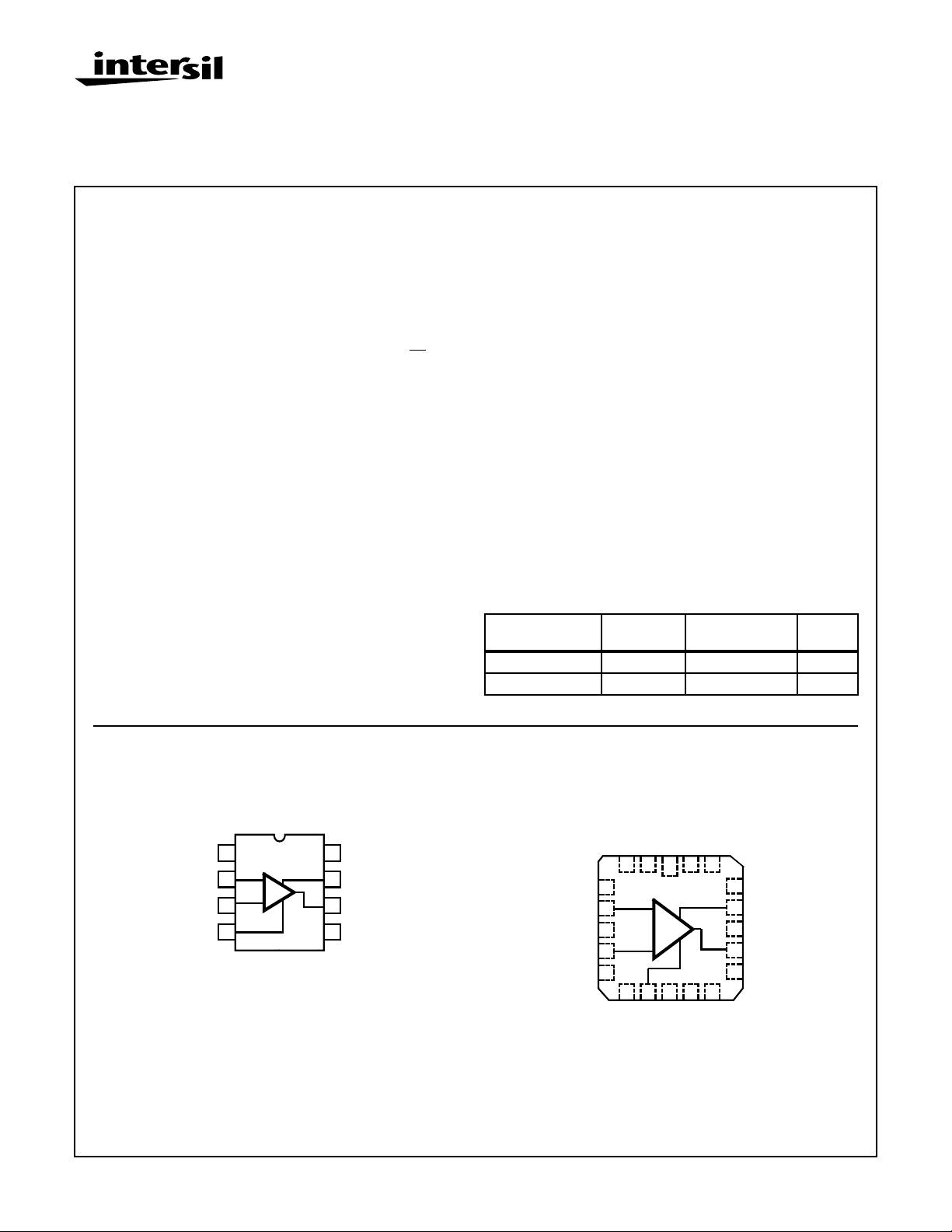
Pinouts
HA-5147/883
(CERDIP)
TOP VIEW
1
BAL
-IN
2
-
+IN
V-
CAUTION: These devices are sensitive to electrostatic discharge; follow proper IC Handling Procedures.
1-888-INTERSIL or 321-724-7143
+
3
4
| Copyright © Intersil Corporation 1999
8
BAL
7
V+
6
OUT
NC
5
1
NC
-IN
NC
+IN
NC
HA-5147/883
(CLCC)
TOP VIEW
NC
BALNCNC
3212019
4
5
6
7
8
+
9101112
NCV-NC
BAL
18
NC
V+
17
16
NC
OUT
15
NC
14
13
NC
NC
Spec Number 511009-883
File Number 3715.2

HA-5147/883
Absolute Maximum Ratings Thermal Information
Voltage Between V+ and V- Terminals. . . . . . . . . . . . . . . . . . . . 44V
Differential Input Voltage (Note 1). . . . . . . . . . . . . . . . . . . . . . . .0.7V
Voltage at Either Input Terminal . . . . . . . . . . . . . . . . . . . . . . V+ to V-
Input Current. . . . . . . . . . . . . . . . . . . . . . . . . . . . . . . . . . . . . . .25mA
Output Current . . . . . . . . . . . . . . . . . . . Full Short Circuit Protection
ESD Rating. . . . . . . . . . . . . . . . . . . . . . . . . . . . . . . . . . . . . . <2000V
Operating Conditions
Temperature Range . . . . . . . . . . . . . . . . . . . . . . . . . -55oC to 125oC
Supply Voltage . . . . . . . . . . . . . . . . . . . . . . . . . . . . . . . . . . . . . . . . . ±15V
V
≤ 1/2 (V+ - V-)
INCM
RL≥ 600Ω
CAUTION: Stresses above those listed in “Absolute Maximum Ratings” may cause permanent damage to the device. This is a stress only rating and operation
of the device at these or any other conditions above those indicated in the operational sections of this specification is not implied.
NOTES:
1. For differential input voltages greater than 0.7V, the input current must be limited to 25mA to protect the back-to-back input diodes.
2. θJA is measured with the component mounted on an evaluation PC board in free air.
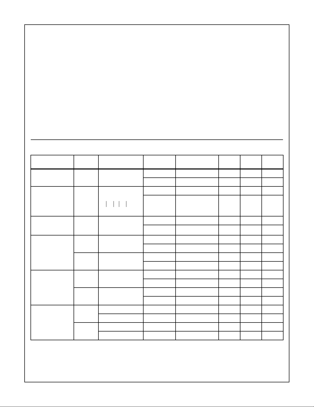
TABLE 1. DC ELECTRICAL PERFORMANCE SPECIFICATIONS
Device Tested at: V
PARAMETER SYMBOL CONDITIONS
Input Offset Voltage V
Input Bias Current I
SUPPLY
= ±15V, R
IO
B
SOURCE
= 50Ω, R
LOAD
= 100kΩ, V
VCM = 0V 1 25 -100 100 µV
VCM = 0V,
RS = 10kΩ, 50Ω
+I
+
BI–B
------------------------------
2
Thermal Resistance (Typical, Note 2) θJA (oC/W) θJC (oC/W)
CERDIP Package . . . . . . . . . . . . . . . . 115 28
CLCC Package . . . . . . . . . . . . . . . . . . 65 15
Package Power Dissipation Limit at 75oC for TJ≤ 175oC
CERDIP Package . . . . . . . . . . . . . . . . . . . . . . . . . . . . . . . 870mW
CLCC Package . . . . . . . . . . . . . . . . . . . . . . . . . . . . . . . . . .1.54W
Package Power Dissipation Derating Factor Above 75oC
CERDIP Package . . . . . . . . . . . . . . . . . . . . . . . . . . . . .8.7mW/oC
CLCC Package . . . . . . . . . . . . . . . . . . . . . . . . . . . . . .15.4mW/oC
Maximum Junction Temperature (TJ) . . . . . . . . . . . . . . . . . . . 175oC
Maximum Storage Temperature Range . . . . . . . . . .-65oC to 150oC
Maximum Lead Temperature (Soldering 10s) . . . . . . . . . . . . . 300oC
= 0V, Unless Otherwise Specified.
OUT
GROUP A
SUBGROUPS TEMP. (oC) MIN MAX UNITS
2, 3 125, -55 -300 300 µV
1 25 - 80 nA
2, 3 125, -55 - 150 nA
Input Offset Current I
Common Mode
+CMR V+ = +4.7V,
Range
Large Signal Voltage
+A
Gain
Common Mode
+CMRR ∆VCM = +11V 1 25 100 - dB
Rejection Ratio
-CMRR ∆VCM = -11V 1 25 100 - dB
VCM = 0V,
IO
+RS = 10kΩ,
-RS = 10kΩ
V- = -25.3V
-CMR V+ = +25.3V,
V- = -4.7V
V
VOL
= 0V and +10V,
OUT
RL = 2kΩ
-A
VOL
V
= 0V and -10V,
OUT
RL = 2kΩ
∆VCM = +10V 2, 3 125, -55 100 - dB
∆VCM = -10V 2, 3 125, -55 100 - dB
1 25 -75 75 nA
2, 3 125, -55 -135 135 nA
1 25 10.3 - V
2, 3 125, -55 10.3 - V
1 25 - -10.3 V
2, 3 125, -55 - -10.3 V
4 25 700 - kV/V
5, 6 125, -55 300 - kV/V
4 25 700 - kV/V
5, 6 125, -55 300 - kV/V
Spec Number 511009-883
2

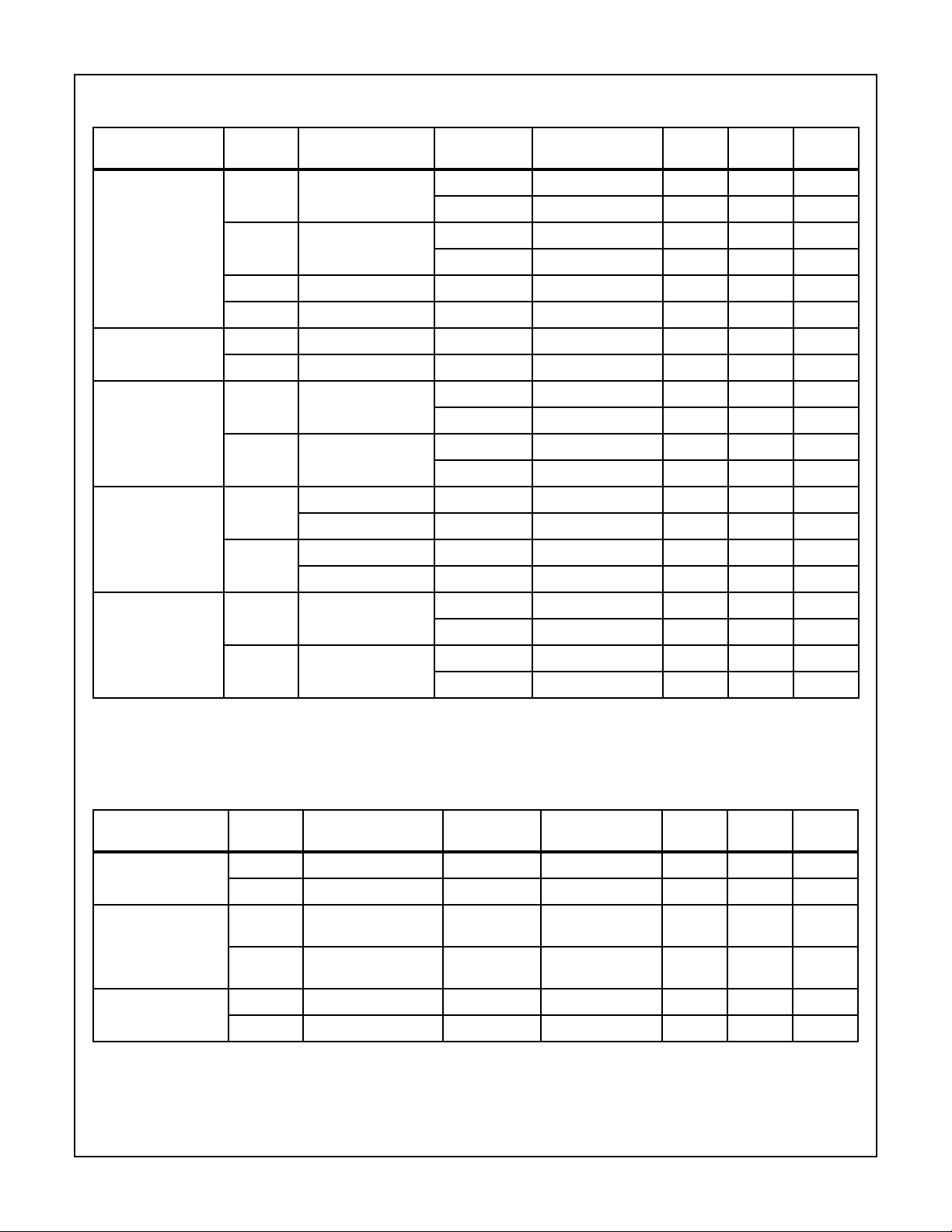
TABLE 1. DC ELECTRICAL PERFORMANCE SPECIFICATIONS (Continued)
Device Tested at: V
SUPPLY
= ±15V, R
SOURCE
PARAMETER SYMBOL CONDITIONS
= 50Ω, R
HA-5147/883
= 100kΩ, V
LOAD
GROUP A
SUBGROUPS TEMP. (oC) MIN MAX UNITS
= 0V, Unless Otherwise Specified.
OUT
Output Voltage Swing +V
OUT1RL
= 2kΩ 4 25 11.5 - V
5, 6 125, -55 11.5 - V
-V
OUT1RL
= 2kΩ 4 25 - -11.5 V
5, 6 125, -55 - -11.5 V
+V
-V
Output Current +I
Quiescent Power
Supply Current
OUT2RL
OUT2RL
OUT
-I
OUT
+I
CC
-I
CC
= 600Ω 42510-V
= 600Ω 4 25 - -10 V
V
= -10V 4 25 16.5 - mA
OUT
V
= +10V 4 25 - -16.5 mA
OUT
V
OUT
=0V,I
= 0mA 1 25 - 4 mA
OUT
2, 3 125, -55 - 4 mA
V
OUT
=0V,I
= 0mA 1 25 -4 - mA
OUT
2, 3 125, -55 -4 - mA
Power Supply
Rejection Ratio
Offset Voltage
Adjustment
+PSRR ∆V
-PSRR ∆V
= +14V 1 25 86 - dB
SUP
∆V
= +13.5V 2, 3 125, -55 86 - dB
SUP
= +14V 1 25 86 - dB
SUP
∆V
= +13.5V 2, 3 125, -55 86 - dB
SUP
+VIOAdj Note 3 1 25 VIO-1 - mV
2, 3 125, -55 VIO-1 - mV
-VIOAdj Note 3 1 25 VIO+1 - mV
2, 3 125, -55 VIO+1 - mV
NOTE:
3. Offset adjustment range is [VIO(Measured) ±1mV] minimum referred to output. This test is for functionality only to assure adjustment
through 0V.
TABLE 2. AC ELECTRICAL PERFORMANCE SPECIFICATIONS
Device Tested at: V
SUPPLY
= ±15V, R
SOURCE
PARAMETER SYMBOL CONDITIONS
Slew Rate +SR V
-SR V
Rise and Fall Time t
r
= -3V to +3V 7 25 28 - V/µs
OUT
= +3V to -3V 7 25 28 - V/µs
OUT
V
= 0 to +200mV
OUT
10% ≤ tr≤ 90%
t
V
f
= 0 to -200mV
OUT
10% ≤ tf≤ 90%
Overshoot +OS V
-OS V
= 0 to +200mV 7 25 - 40 %
OUT
= 0 to -200mV 7 25 - 40 %
OUT
= 50Ω, R
LOAD
= 2kΩ, C
LOAD
= 50pF, A
= +10V/V, Unless Otherwise Specified.
VCL
GROUP A
SUBGROUPS TEMP. (oC) MIN MAX UNITS
7 25 - 50 ns
7 25 - 50 ns
Spec Number 511009-883
3
 Loading...