Intersil Corporation HA-5134 Datasheet

HA-5134
Data Sheet August 1998 File Number 2926.3
4MHz, Precision, Quad Operational
Amplifier
The HA-5134 is a precision quad operational amplifier that is
pin compatible with the OP-400, LT1014, OP11, RM4156,
and LM148 as well as the HA-4741. Each amplifier features
guaranteed maximum values for offset voltage of 200µV,
offset voltage drift of 2µV/
the full temperature range while CMRR/PSRR is guaranteed
greater than 94dB and A
over the full temperature range.
Precision performance of the HA-5134 is enhanced by a
noise voltage density of 7nV/√
density of 1pA/√
Hz at 1kHz and channel separation of
120dB. Each unity-gain stable quad amplifier is fabricated
using the dielectric isolation process to assure performance
in the most demanding applications.
The HA-5134 is ideal for compact circuits such as
instrumentation amplifiers, state-variable filters, and lowlevel transducer amplifiers. Other applications include
precision data acquisition, precision integrators, and
accurate threshold detectors in designs where board space
is a limitation.
Formilitary gradeproduct,refertotheHA-5134/883 data sheet.
o
C,and offset current of 75nA over
is guaranteed above 500kV/V
VOL
Hz at 1kHz, noise current
Features
• Low Offset Voltage . . . . . . . . . . . . . . . . . . . . 200µV(Max)
o
• Low Offset Voltage Drift . . . . . . . . . . . . . . . 2µV/
C(Max)
• High Channel Separation. . . . . . . . . . . . . . . . . . . . 120dB
• Low Noise. . . . . . . . . . . . . . . . . . . . . . . . . . . . . . 7nV/√
Hz
• Unity Gain Bandwidth. . . . . . . . . . . . . . . . . . . . . . . . 4MHz
• High CMRR/PSRR. . . . . . . . . . . . . . . . . . . . . 120dB (Typ)
Applications
• Instrumentation Amplifiers
• State-Variable Filters
• Precision Integrators
• Threshold Detectors
• Precision Data Acquisition Systems
• Low-Level Transducer Amplifiers
Pinout
HA-5134
(CERDIP)
TOP VIEW
Ordering Information
TEMP.
PART NUMBER
HA1-5134-5 0 to 75 14 Ld CERDIP F14.3
RANGE (oC) PACKAGE
PKG.
NO.
OUT 1
-IN 1
+IN 1
V+
+IN 2
-IN 2
OUT 2
1
2
-
1
+
3
4
5
+
2
-
6
7
14
OUT 4
13
-
4
+
+
3
-
-IN 4
12
+IN 4
11
V-
10
+IN 3
9
-IN 3
8
OUT 3
1
CAUTION: These devices are sensitive to electrostatic discharge; follow proper IC Handling Procedures.
1-888-INTERSIL or 321-724-7143
| Copyright © Intersil Corporation 1999

HA-5134
Absolute Maximum Ratings Thermal Information
Voltage Between V+ and V- Terminals. . . . . . . . . . . . . . . . . . . . 40V
Differential Input Voltage (Note 2) . . . . . . . . . . . . . . . . . . . . . . . . 6V
Output Current. . . . . . . . . . . . . . . . . . . . Full Short Circuit Protection
Operating Conditions
Temperature Range
HA-5134-5 . . . . . . . . . . . . . . . . . . . . . . . . . . . . . . . . 0oC to 75oC
CAUTION: Stresses above those listed in “Absolute Maximum Ratings” may cause permanent damage to the device. This is a stress only rating and operation of the
device at these or any other conditions above those indicated in the operational sections of this specification is not implied.
NOTES:
1. θJA is measured with the component mounted on an evaluation PC board in free air.
2. For differential input voltages greater than 6V, the input current must be limited to 25mA to protect the back-to-back input diodes.
3. Maximum power dissipation, including output load, must be designed to maintain the maximum junction temperature below 175oC.
Thermal Resistance (Typical, Note 1) θJA (oC/W) θJC (oC/W)
CERDIP Package. . . . . . . . . . . . . . . . . 80 30
Maximum Junction Temperature (Note 3) . . . . . . . . . . . . . . . . 175oC
Maximum Storage Temperature Range. . . . . . . . . . -65oC to 150oC
Maximum Lead Temperature (Soldering 10s) . . . . . . . . . . . . 300oC
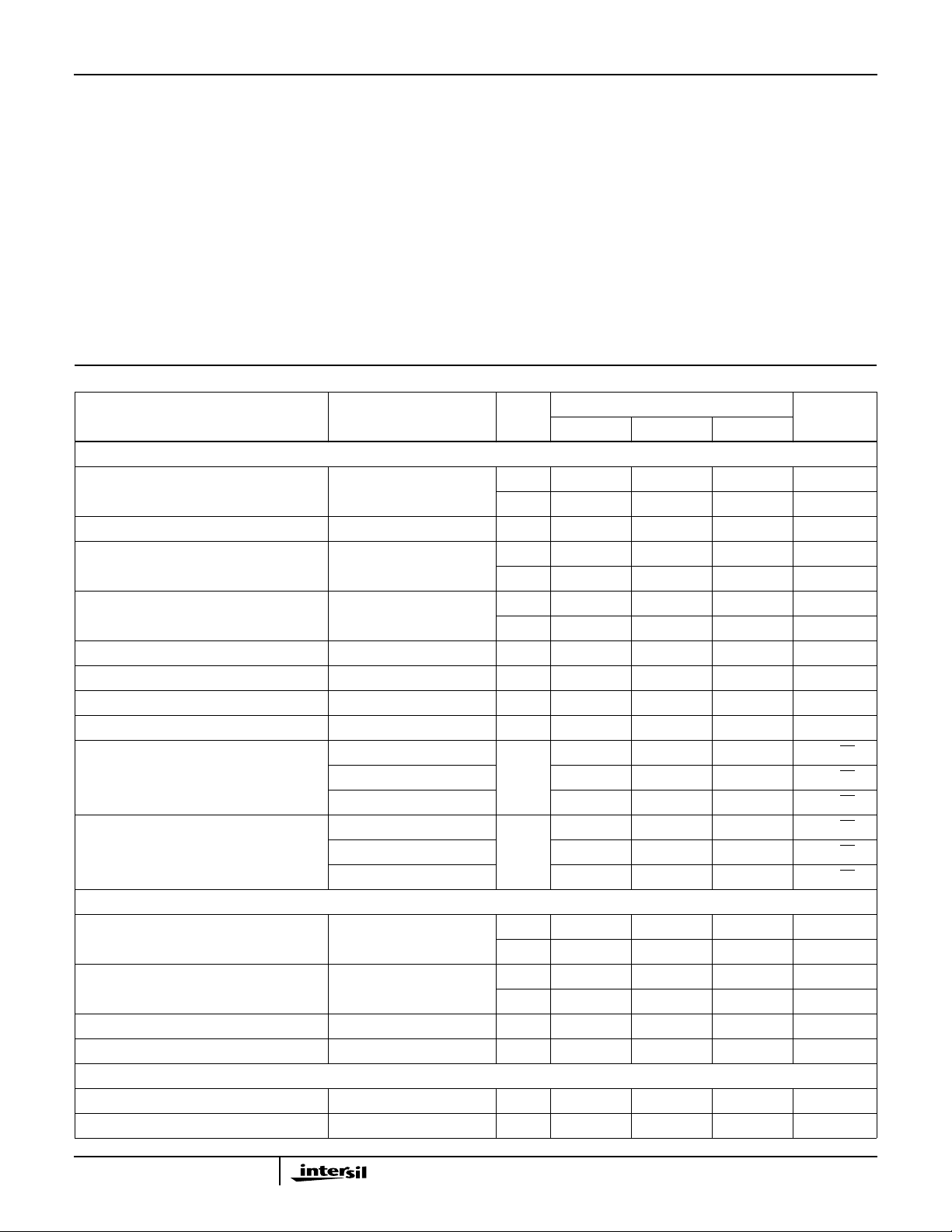
Electrical Specifications V
PARAMETER TEST CONDITIONS
INPUT CHARACTERISTICS
Offset Voltage 25 - 50 200 µV
Average Offset Voltage Drift Full - 0.3 2 µV/oC
Bias Current 25 - ±10 ±50 nA
Offset Current 25 - 10 50 nA
Average Offset Current Drift Full - 0.05 - nA/oC
Common Mode Range Full ±10 - - V
Differential Input Resistance 25 - 30 - MΩ
Input Noise Voltage 0.1Hz to 10Hz 25 - 0.2 - µV
Input Noise Voltage Density f = 10Hz 25 - 10 - nV/√Hz
Input Noise Current Density f = 10Hz 25 - 3 - pA/√Hz
TRANSFER CHARACTERISTICS
Large Signal Voltage Gain V
Common Mode Rejection Ratio VCM = ±10V 25 100 120 - dB
Minimum Stable Gain 25 1 - - V/V
Unity-Gain Bandwidth 25 - 4 - MHz
OUTPUT CHARACTERISTICS
Output Voltage Swing Full 12 13.5 - V
Output Current 25 - 20 - mA
= ±15V, RL = 2kΩ, CL = 50pF, RS≤ 100Ω, Unless Otherwise Specified
SUPPLY
TEMP
(oC)
Full - 75 350 µV
Full - ±20 ±75 nA
Full - 15 75 nA
f = 100Hz - 7.5 - nV/√Hz
f = 1kHz - 7 - nV/√Hz
f = 100Hz - 1.5 - pA/√Hz
f = 1kHz - 1 - pA/√Hz
= ±10V 25 800 1200 - kV/V
OUT
Full 500 750 - kV/V
Full 94 115 - dB
HA-5134-5
UNITSMIN TYP MAX
P-P
2

HA-5134
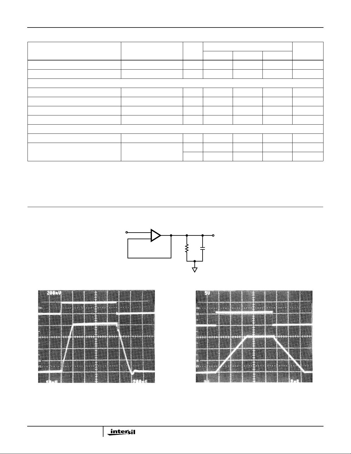
Electrical Specifications V
PARAMETER TEST CONDITIONS
Full Power Bandwidth (Note 4) 25 12 16 - kHz
Channel Separation (Note 7) V
TRANSIENT RESPONSE (Note 5)
Rise Time AV = +1, V
Slew Rate AV = +1 25 0.75 1.0 - V/µs
Overshoot AV = +1 25 - 20 40 %
Settling Time (Note 6) 25 - 13 - µs
POWER SUPPLY CHARACTERISTICS
Supply Current All Amps Full - 6.5 8 mA
Power Supply Rejection Ratio VS = ±5V to ±18V 25 100 120 - dB
NOTES:
4. Full power bandwidth guaranteed based on slew rate measurement using: .
5. Refer to Test Circuits section of the data sheet.
6. Specified to 0.01% of a 10V step, AV = -1.
7. Guaranteed but not tested.
= ±15V, RL = 2kΩ, CL = 50pF, RS≤ 100Ω, Unless Otherwise Specified (Continued)
SUPPLY
PEAK
HA-5134-5
;V
PEAK
TEMP
(oC)
= ±10V 25 120 136 - dB
OUT
= 200mV 25 - 200 400 ns
OUT
Full 94 115 - dB
Slew Rate
FPBW
------------------------------ -
2π V
UNITSMIN TYP MAX
10V==
Test Circuits and Waveforms
FIGURE 1. SLEW RATE AND TRANSIENT RESPONSE TEST CIRCUIT
IN
+
-
2kΩ
OUT
50pF
Vertical: 50mV/Div., Horizontal: 200ns/Div.
TA = 25oC, VS = ±15V, AV = +1, RL = 2kΩ, CL = 50pF
SMALL SIGNAL RESPONSE
3
Vertical: 2V/Div., Horizontal: 2µs/Div.
TA = 25oC, VS = ±15V, AV = +1, RL = 2kΩ, CL = 50pF
LARGE SIGNAL RESPONSE
 Loading...