Intersil Corporation HA5022-883 Datasheet
256
CAUTION: These devices are sensitive to electrostatic discharge; follow proper IC Handling Procedures.
http://www.intersil.com or 407-727-9207
| Copyright © Intersil Corporation 1999
HA5022/883
Dual 125MHz Video Current
Feedback Amplifier with Disable
Description
The HA5022/883 is a dual version of the popular Intersil HA-
5020. It features wide bandwidth and high slew rate, and is
optimized for video applications and gains between 1 and
10. It is a current feedback amplifier and thus yields less
bandwidth degradation at high closed loop gains than voltage feedback amplifiers.
The low differential gain and phase, 0.1dB gain flatness, and
ability to drive two back terminated 75Ω cables, make this
amplifier ideal for demanding video applications.
The HA5022/883 also features a disable function that significantly reduces supply current while forcing the output to a
true high impedance state. This functionality allows 2:1 video
multiplexers to be implemented with a single IC.
The current feedback design allows the user to take advantage of the amplifier’s bandwidth dependency on the feedback resistor. By reducing R
F
, the bandwidth can be
increased to compensate for decreases at higher closed
loop gains or heavy output loads.
Ordering Information
PART
NUMBER
TEMPERATURE
RANGE PACKAGE
HA5022MJ/883 -55oC to +125oC 16 Lead CerDIP
Features
• This Circuit is Processed in Accordance to MIL-STD883 and is Fully Conformant Under the Provisions of
Paragraph 1.2.1.
• Dual Version of HA-5020
• Individual Output Enable/Disable
• Wide Unity Gain Bandwidth . . . . . . . . . . . . . . . 125MHz
• Slew Rate . . . . . . . . . . . . . . . . . . . . . . . . . . . . . . 475V/µs
• Differential Gain. . . . . . . . . . . . . . . . . . . . . . . . . . . 0.03%
• Differential Phase. . . . . . . . . . . . . . . . . . . . . . . 0.03 Deg.
• Supply Current (per Amplifier) . . . . . . . . . . . . . . .7.5mA
• Crosstalk Rejection at 10MHz. . . . . . . . . . . . . . . . -60dB
• ESD Protection. . . . . . . . . . . . . . . . . . . . . . . . . . . . 2000V
• Guaranteed Specifications at ±5V Supplies
Applications
• Video Multiplexers; Video Switching and Routing
• Video Gain Block
• Video Distribution Amplifier/RGB Amplifier
• Flash A/D Driver
• Current to Voltage Converter
• Radar and Imaging Systems
• Medical Imaging
January 1995
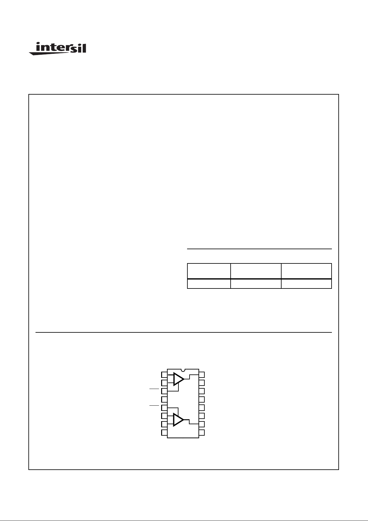
Pinout
HA5022/883
(CERDIP)
TOP VIEW
14
15
16
9
13
12
11
10
1
2
3
4
5
7
6
8
-IN1
+IN1
DIS1
VDIS2
+IN2
NC
-IN2
OUT1
NC
V+
NC
NC
OUT2
NC
NC
+
-
+
-
Spec Number 511107-883
File Number 3729.1

257
Specifications HA5022/883
Spec Number 511107-883
Absolute Maximum Ratings Thermal Information
Voltage Between V+ and V- . . . . . . . . . . . . . . . . . . . . . . . . . . . . 36V
Differential Input Voltage . . . . . . . . . . . . . . . . . . . . . . . . . . . . . . 10V
Voltage at Either Input Terminal . . . . . . . . . . . . . . . . . . . . . . V+ to V-
Output Current . . . . . . . . . . . . . . . . . . . . Full Short Circuit Protected
Junction Temperature. . . . . . . . . . . . . . . . . . . . . . . . . . . . . . +175oC
ESD Rating. . . . . . . . . . . . . . . . . . . . . . . . . . . . . . . . . . . . . .< 2000V
Storage Temperature Range . . . . . . . . . . . . . .-65oC ≤ TA≤ +150oC
Lead Temperature (Soldering 10s). . . . . . . . . . . . . . . . . . . . +300oC
Thermal Resistance θ
JA
θ
JC
CerDIP Package . . . . . . . . . . . . . . . . . 75oC/W 20oC/W
Maximum Package Power Dissipation at +75oC
CerDIP Package . . . . . . . . . . . . . . . . . . . . . . . . . . . . . . . . .1.33W
Package Power Dissipation Derating Factor above +75oC
CerDIP Package . . . . . . . . . . . . . . . . . . . . . . . . . . . . .13.3mW/oC
CAUTION: Stresses above those listed in “Absolute Maximum Ratings” may cause permanent damage to the device. This is a stress only rating and operation
of the device at these or any other conditions above those indicated in the operational sections of this specification is not implied.
Operating Conditions
Operating Supply Voltage (±VS) . . . . . . . . . . . . . . . . . . . . ±5V to ±15V
Operating Temperature Range. . . . . . . . . . . . .-55oC ≤ TA≤ +125oC
V
INCM
≤ 1/2(V+ - V-) RL≥ 50Ω
V
DISABLE
= V+ or 0V RF= 1kΩ
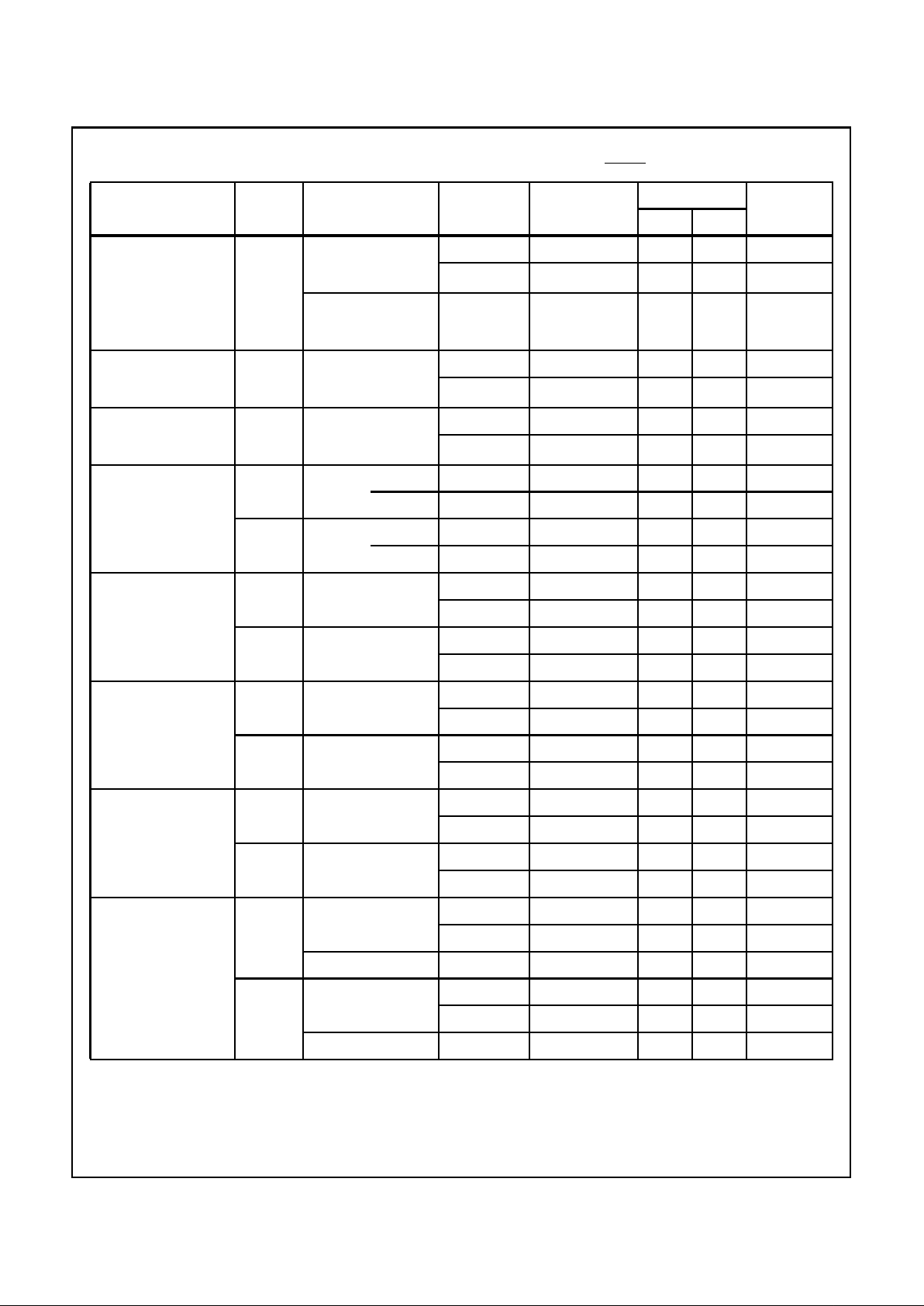
TABLE 1. DC ELECTRICAL PERFORMANCE CHARACTERISTICS
Device Tested at: V
SUPPLY
= ±5V, AV= +1, RF=1kΩ, R
SOURCE
= 0Ω, RL = 400Ω, V
OUT
= 0V, V
DISABLE
= V+, Unless Otherwise Specified.
PARAMETERS SYMBOL CONDITIONS
GROUP A
SUBGROUPS TEMPERATURE
LIMITS
UNITSMIN MAX
Input Offset Voltage V
IO
VCM= 0V 1 +25oC-33mV
2, 3 +125
o
C, -55oC-5 5 mV
Common Mode
Rejection Ratio
CMRR ∆VCM= ±2.5V
V+ = 2.5V, V- = -7.5V
V+ = 7.5V, V- = -2.5V
1 +25oC53- dB
2 +125
o
C38- dB
∆VCM= ±2.25V
V+ = 2.75V , V- = -7.25V
V+ = 7.25V , V- = -2.75V
3 -55oC38-dB
Power Supply
Rejection Ratio
PSRR ∆V
SUP
= ±1.5V
V+ = 6.5V, V- = -5V
V+ = 3.5V, V- = -5V
1 +25oC60- dB
2, 3 +125
o
C, -55oC55 - dB
Delta Input Offset
Voltage
Between Channels
∆V
IO
VCM = 0 1 +25oC - 3.5 mV
2,3 +125oC, -55oC - 3.5 mV
Non-Inverting Input (+IN)
Current
I
BSP
VCM= 0V 1 +25oC-88µA
2, 3 +125
o
C, -55oC -20 20 µA
+IN Current Common
Mode Sensitivity
CMS
IBP
∆VCM= ±2.5V
V+ = 2.5V, V- = -7.5V
V+ = 7.5V, V- = -2.5V
1 +25oC - 0.15 µA/V
2 +125
o
C - 2.0 µA/V
∆VCM= ±2.25V
V+ = 2.75V , V- = -7.25V
V+ = 7.25V , V- = -2.75V
3 -55oC - 2.0 µA/V
∆Inverting Input (-IN)
Current Between
Channels
∆I
BSN
VCM = 0 1 +25oC -15 15 µA
2, 3 +125
o
C -30 30 µA
Inverting Input (-IN)
Current
I
BSN
VCM= 0V 1 +25oC -12 12 µA
2, 3 +125oC, -55oC -30 30 µA
258
Specifications HA5022/883
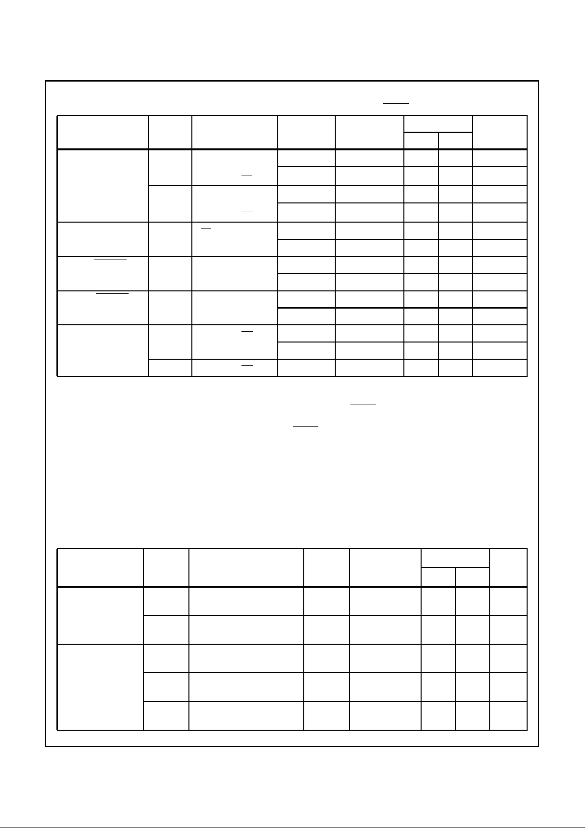
-IN Current Common
Mode Sensitivity
CMS
IBN
∆VCM= ±2.5V
V+ = 2.5V, V- = -7.5V
V+ = 7.5V, V- = -2.5V
1 +25oC - 0.4 µA/V
2 +125
o
C-5µA/V
∆VCM= ±2.25V
V+ = 2.75V , V- = -7.25V
V+ = 7.25V , V- = -2.75V
3 -55oC-5µA/V
-IN Current Power
Supply Sensitivity
PSS
IBN
∆V
SUP
= ±1.5V
V+ = 6.5V, V- = -5V
V+ = 3.5V, V- = -5V
1 +25oC - 0.2 µA/V
2, 3 +125
o
C, -55oC - 0.5 µA/V
+IN Current Power
Supply Sensitivity
PSS
IBP
∆V
SUP
= ±1.5V
V+ = 6.5V, V- = -5V
V+ = 3.5V, V- = -5V
1 +25oC - 0.1 µA/V
2, 3 +125oC, -55oC - 0.3 µA/V
Output Voltage
Swing
V
OP
AV = +1
RL = 150Ω
VIN= -3V 1 +25oC 2.5 - V
V
IN
= -3V 2, 3 +125oC, -55oC 2.5 - V
V
ON
AV = +1
RL = 150Ω
VIN= +3V 1 +25oC - -2.5 V
V
IN
= +3V 2, 3 +125oC, -55oC - -2.5 V
Short Circuit Output
Current
+I
SC
VIN= ±2.5V
V
OUT
=0V
1 +25oC50-mA
2, 3 +125
o
C, -55oC50 - mA
-I
SC
VIN= ±2.5V
V
OUT
=0V
1 +25oC - -40 mA
2, 3 +125
o
C, -55oC - -40 mA
Output Current +I
OUT
Note 1 1 +25oC20-mA
2, 3 +125
o
C, -55oC 16.6 - mA
-I
OUT
Note 1 1 +25oC - -20 mA
2, 3 +125
o
C, -55oC - -16.6 mA
Quiescent Power
Supply Current
I
CC
RL= 400Ω 1 +25oC - 10 mA/Op Amp
2, 3 +125
o
C, -55oC - 10 mA/Op Amp
I
EE
RL= 400Ω 1 +25oC -10 - mA/Op Amp
2, 3 +125
o
C, -55oC -10 - mA/Op Amp
Transimpedance +A
ZOL1RL
= 400Ω
V
OUT
= ±2.5V
1 +25oC1-MΩ
2 +125
o
C 0.5 - MΩ
V
OUT
= ±2.25V 3 -55oC 0.5 - MΩ
-A
ZOL1RL
= 400Ω
V
OUT
= ±2.5V
1 +25oC1-MΩ
2 +125oC 0.5 - MΩ
V
OUT
= ±2.25V 3 -55oC 0.5 - MΩ
TABLE 1. DC ELECTRICAL PERFORMANCE CHARACTERISTICS (Continued)
Device Tested at: V
SUPPLY
= ±5V, AV= +1, RF=1kΩ, R
SOURCE
= 0Ω, RL = 400Ω, V
OUT
= 0V, V
DISABLE
= V+, Unless Otherwise Specified.
PARAMETERS SYMBOL CONDITIONS
GROUP A
SUBGROUPS TEMPERATURE
LIMITS
UNITSMIN MAX
Spec Number 511107-883
259
Specifications HA5022/883
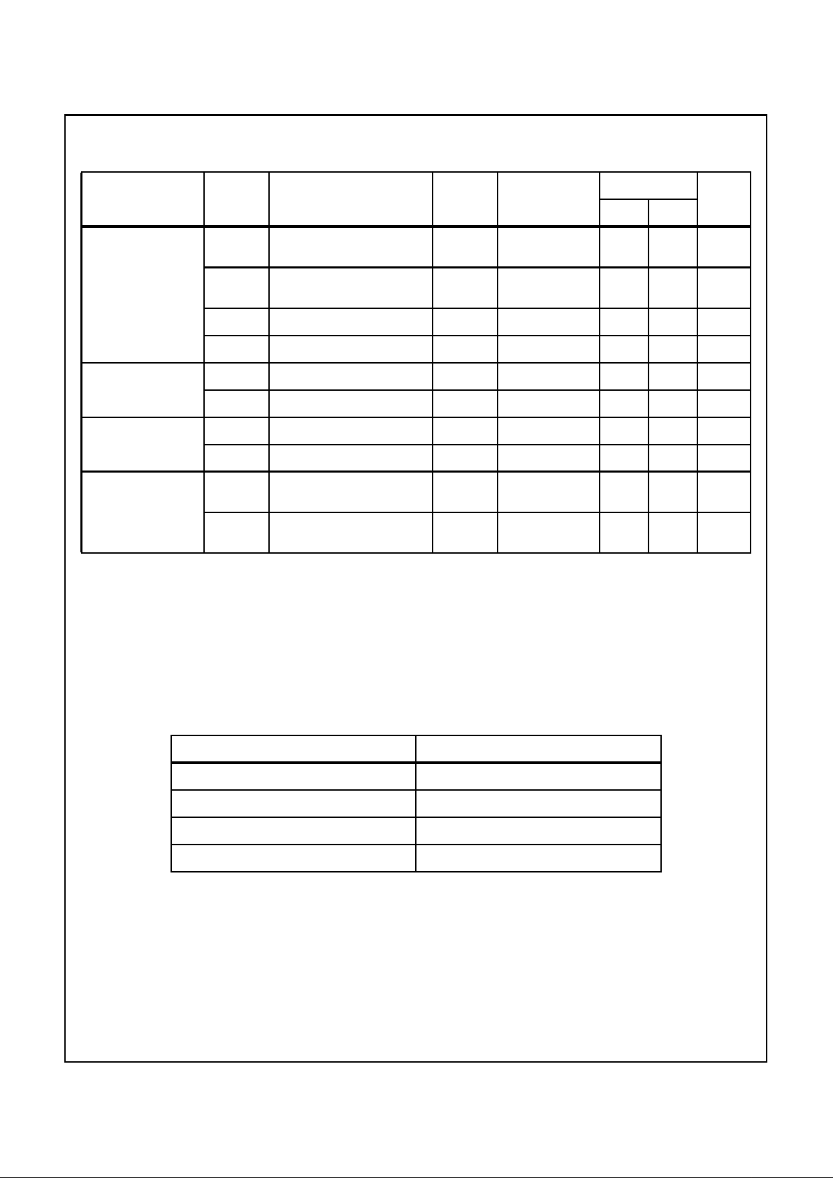
Disabled Output Current +I
LEAK
VIN= 0V,
V
OUT
= +2.5V
RL= Open, V
DIS
=0V
1 +25oC-1µA
2, 3 +125
o
C, -55oC- 2 µA
-I
LEAK
VIN= 0V,
V
OUT
= -2.5V
RL= Open, V
DIS
=0V
1 +25oC-1µA
2, 3 +125oC, -55oC- 2 µA
Disable Pin Input Current I
LOGIC
V
DIS
= 0V 1 +25oC -1.0 - mA
2, 3 +125
o
C, -55oC -1.5 - mA
Minimum DISABLE Pin
Current to Disable
I
DIS
Note 2 1 +25oC - 350 µA
2, 3 +125
o
C, -55oC - 350 µA
Maximum DISABLE Pin
Current to Enable
I
EN
Note 3 1 +25oC20- µA
2, 3 +125
o
C, -55oC20 - µA
Disabled Power Supply
Current
I
CCDIS
RL= Open, V
DIS
= 0V 1 +25oC - 7.5 mA/Op Amp
2, 3 +125
o
C, -55oC - 7.5 mA/Op Amp
I
EEDIS
RL= Open, V
DIS
= 0V 1 +25oC 7.5 - mA/Op Amp
NOTES:
1. Guaranteed from V
OUT
Test with RL= 150Ω, by: I
OUT=VOUT
/150Ω.
2. RL = 100Ω, VIN = 2.5V. This is the minimum current which must be pulled out of the Disable pin in order to disable the output. The output
is considered disabled when -10mV ≤ V
OUT
≤ +10mV.
3. VIN = 0V. This is the maximum current that can be pulled out of the Disable pin with the HA5022/883 remaining enabled. The HA5022/883
is considered disabled when the supply current has decreased by at least 0.5mA.
TABLE 2. AC ELECTRICAL PERFORMANCE CHARACTERISTICS
Table 2 Intentionally Left Blank.
TABLE 3. ELECTRICAL PERFORMANCE CHARACTERISTICS
Device Characterized at: V
SUPPLY
= ±5V, AV = +2, RF= 681Ω, RL = 400Ω, Unless Otherwise Specified.
PARAMETERS SYMBOL CONDITIONS NOTES TEMPERATURE
LIMITS
UNITSMIN MAX
-3dB Bandwidth BW(+1) AV = +1, RF = 1K
V
OUT
= 100mV
RMS
1 +125oC, -55oC 70 - MHz
BW(+2) AV = +2,
V
OUT
= 100mV
RMS
1 +125oC, -55oC 70 - MHz
Gain Flatness GF5 AV = +2, f ≤5MHz
V
OUT
= 100mV
RMS
1 +125oC, -55oC-±0.045 dB
GF10 AV = +2, f ≤10MHz
V
OUT
= 100mV
RMS
1 +125oC, -55oC-±0.085 dB
GF20 AV = +2, f ≤20MHz
V
OUT
= 100mV
RMS
1 +125oC, -55oC-±0.65 dB
TABLE 1. DC ELECTRICAL PERFORMANCE CHARACTERISTICS
(Continued)
Device Tested at: V
SUPPLY
= ±5V, AV= +1, RF=1kΩ, R
SOURCE
= 0Ω, RL = 400Ω, V
OUT
= 0V, V
DISABLE
= V+, Unless Otherwise Specified.
PARAMETERS SYMBOL CONDITIONS
GROUP A
SUBGROUPS TEMPERATURE
LIMITS
UNITSMIN MAX
Spec Number 511107-883
260
Specifications HA5022/883
Slew Rate +SR(+1) AV = +1, RF = 1K
V
OUT
= -2V to +2V
1, 4 +125oC, -55oC 300 - V/µs
-SR(+1) AV = +1, RF = 1K
V
OUT
= +2V to -2V
1, 4 +125oC, -55oC 270 - V/µs
+SR(+2) AV = +2, V
OUT
= -2V to +2V 1, 4 +125oC, -55oC 465 - V/µs
-SR(+2) AV = +2, V
OUT
= +2V to -2V 1, 4 +125oC, -55oC 350 - V/µs
Rise and Fall Time T
R
AV = +2, V
OUT
= -0.5V to -0.5V 1, 2 +125oC, -55oC - 5.5 ns
T
F
AV = +2, V
OUT
=+0.5V to +0.5V 1, 2 +125oC, -55oC - 6.0 ns
Overshoot +OS AV = +2, V
OUT
= -0.5V to +0.5V 1, 3 +125oC, -55oC - 35 %
-OS AV = +2, V
OUT
= +0.5V to -0.5V 1, 3 +125oC, -55oC - 27 %
Propagation Delay +T
P
AV = +2, RF = 681Ω
V
OUT
= 0V to 1V
1, 2 +125oC, -55oC - 10 ns
-T
P
AV = +2, RF = 681Ω
V
OUT
= 1V to 0V
1, 2 +125oC, -55oC - 9.5 ns
NOTES:
1. Parameters listed in Table 3 are controlled via design or process parameters and are not directly tested at final production. These parameters are lab characterized upon initial design release, or upon design changes. These parameters are guaranteed by characterization
based upon data from multiple production runs which reflect lot-to-lot and within lot variation.
2. Measured between 10% and 90% points.
3. For 200ps input transition times. Overshoot decreases as input transition times increase, especially for AV= +1. Please refer to
Performance Curves.
4. Measured between 25% and 75% points.
TABLE 4. ELECTRICAL TEST REQUIREMENTS
MIL-STD-883 TEST REQUIREMENTS SUBGROUPS (SEE TABLE 1)
Interim Electrical Parameters (Pre Burn-In) 1
Final Electrical Test Parameters 1 (Note 1), 2, 3, 4
Group A Test Requirements 1, 2, 3, 4
Groups C and D Endpoints 1
NOTE:
1. PDA applies to Subgroup 1 only.
TABLE 3. ELECTRICAL PERFORMANCE CHARACTERISTICS (Continued)
Device Characterized at: V
SUPPLY
= ±5V, AV = +2, RF= 681Ω, RL = 400Ω, Unless Otherwise Specified.
PARAMETERS SYMBOL CONDITIONS NOTES TEMPERATURE
LIMITS
UNITSMIN MAX
Spec Number 511107-883

261
HA5022/883
Test Circuits and Waveforms
FIGURE 1. TEST CIRCUIT (Applies to Table 1)
FIGURE 2. TEST CIRCUIT FOR TRANSIMPEDANCE MEASUREMENTS
FIGURE 3. SMALL SIGNAL PULSE RESPONSE CIRCUIT
FIGURE 4. LARGE SIGNAL PULSE RESPONSE CIRCUIT
FIGURE 5. SMALL SIGNAL RESPONSE
Vertical Scale: V
IN
= 100mV/Div., V
OUT
= 100mV/Div.
Horizontal Scale: 20ns/Div.
FIGURE 6. LARGE SIGNAL RESPONSE
Vertical Scale: VIN = 1V/Div., V
OUT
= 1V/Div.
Horizontal Scale: 50ns/Div.
V+
ICC
10 0.1
13
DUT
-
+
1, 7
2, 6
4
1K
V
IN
-
+
HA-5177
200pF
100K (0.01%)
V
Z
V
X
x100
-
+
470pF
V
IO
=
V
X
100
+I
BIAS
=
V
Z
100K
10 0.1
V-
I
EE
-I
BIAS
=
V
X
50K
K6
400
100
V
OUT
NOTE: All Resistors = ±1% (Ω)
All Capacitors = ±10% (µF)
Unless Otherwise Noted
16, 10
+
+
0.1
100
0.1
K1
NC
1K
0.1
1K
510
510
0.1
K2
2
1
K2 = POSITION 1:
K2 = POSITION 2:
0.1
Chip Components Recommended
K5
50
K3
3, 5
0.1
V
D
NC
+
-
50
50
DUT
HP4195
NETWORK
ANALYZER
V
IN
V
OUT
R
L
RF, 1K
100Ω
50Ω
+
-
DUT
V
IN
V
OUT
R
L
RF, 681
400Ω
50Ω
+
-
DUT
R
I
681Ω
Spec Number 511107-883
262
HA5022/883
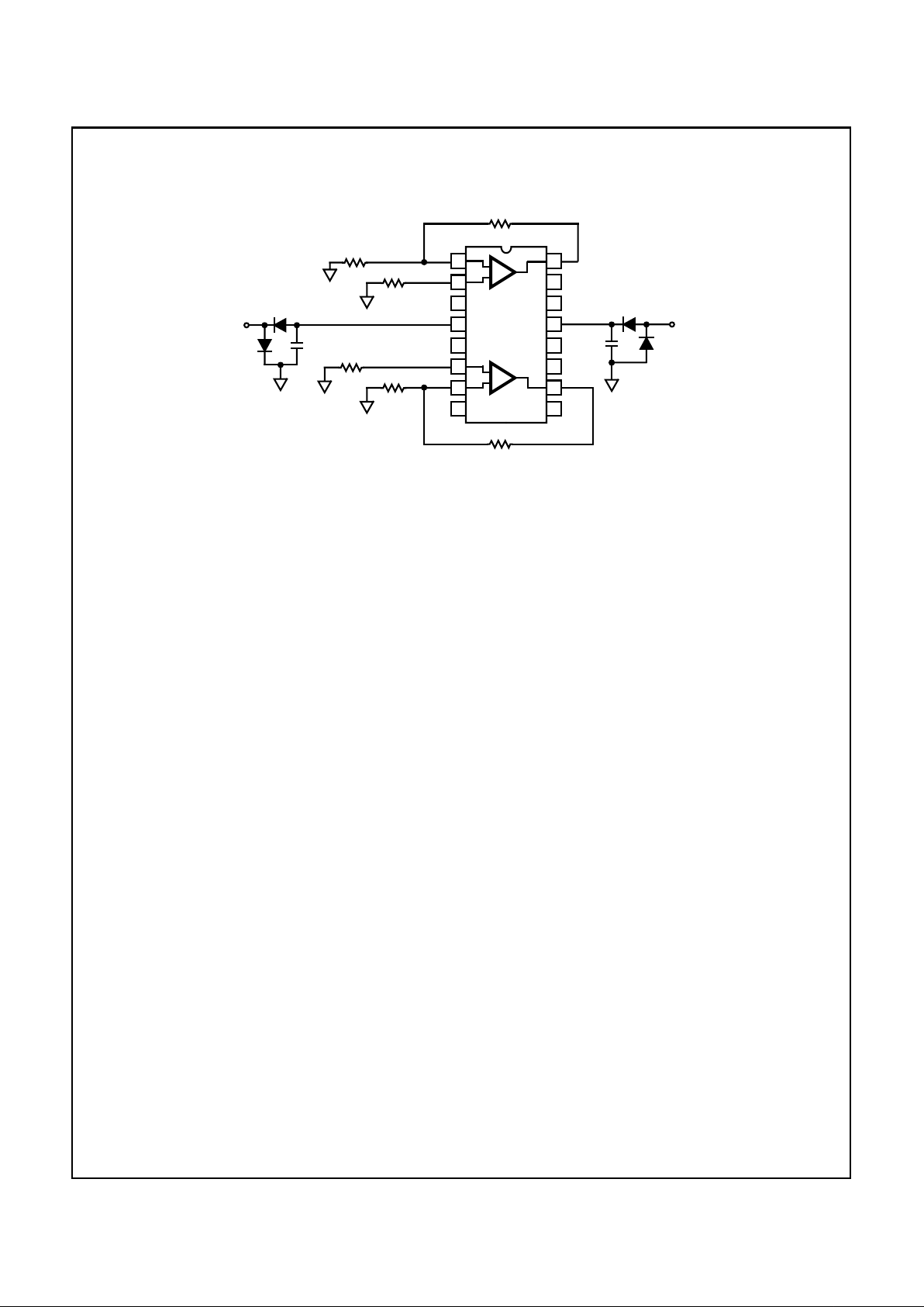
Burn-In Circuit
HA5022MJ/883 CERAMIC DIP
NOTES:
R1 = R2 = R4 = R5 = 1kΩ, ±5% (Per Socket)
R3 = R6 = 10kΩ, ±5% (Per Socket)
C1 = C2 = 0.01µF (Per Socket) or 0.1µF (Per Row) Minimum
D1 = D2 = 1N4002 or Equivalent (Per Board)
D3 = D4 = 1N4002 or Equivalent (Per Socket)
V+ = +5.5V ± 0.5V
V- = -5.5V ± 0.5V
V+
C1 D1
D2 C2
V-
D4 D3
R2
R1
R3
14
15
16
9
13
12
11
10
1
2
3
4
5
7
6
8
R4
R5
R6
+
-
+
-
Spec Number 511107-883
 Loading...