Intersil Corporation HA-5020-883 Datasheet

January 1996
HA-5020/883
100MHz Current Feedback
Video Amplifier with Disable
Features
• This Circuit is Processed in Accordance to MIL-STD883 and is Fully Conformant Under the Provisions of
Paragraph 1.2.1.
• Wide Unity Gain Bandwidth . . . . . . . . . . 105MHz (Min)
• Slew Rate . . . . . . . . . . . . . . . . . . . . . . . . . . . . . . 800V/µs
• Output Current. . . . . . . . . . . . . . . . . . . . . . ±30mA (Min)
• Drives 3.5V into 75Ω
• Differential Gain. . . . . . . . . . . . . . . . . . . . . . . . . .0.025%
• Differential Phase. . . . . . . . . . . . . . . . . . . . . . .0.025 Deg
• Low Input Noise Voltage . . . . . . . . . . . . . . . . 4.5nV/√
Hz
• Low Supply Current. . . . . . . . . . . . . . . . . . . 10mA (Max)
• Wide Supply Range . . . . . . . . . . . . . . . . . . . ±5V to ±15V
• Output Enable/Disable
• High Performance Replacement for EL2020/883
Applications
• Unity Gain Video/Wideband Buffer
• Video Gain Block
• Video Distribution Amp/Coax Cable Driver
• Flash A/D Driver
• Waveform Generator Output Driver
• Current to Voltage Converter; D/A Output Buffer
• Radar Systems
• Imaging Systems
Description
The HA-5020/883 is a wide bandwidth, high slew rate
amplifier optimized for video applications and gains between
1 and 10. Manufactured on Intersil’s Reduced Feature
Complementary Bipolar DI process, this amplifier uses current mode feedback to maintain higher bandwidth at a given
gain than conventional voltage feedback amplifiers. Since it
is a closed loop device, the HA-5020/883 offers better gain
accuracy and lower distortion than open loop buffers.
The HA-5020/883 features low diff erential gain and phase and
will drive two double terminated 75Ω coax cables to video
levels with low distortion. Adding a gain flatness performance
of 0.1dB makes this amplifier ideal for demanding video
applications. The bandwidth and slew rate of the HA-5020/
883 are relatively independent of closed loop gain. The
105MHz unity gain bandwidth only decreases to 77MHz at a
gain of 10. The HA-5020/883 used in place of a conventional
op amp will yield a significant improvement in the speed
power product. To further reduce power , the HA-5020/883 has
a disable function which significantly reduces supply current,
while forcing the output to a true high impedance state. This
allows the outputs of multiple amplifiers to be wire-OR’d into
multiplexer configurations. The device also includes output
short circuit protection and output offset voltage adjustment.
The HA-5020/883 offers significant enhancements over
competing amplifiers, such as the EL2020. Improvements
include unity gain bandwidth, slew rate, video performance,
lower supply current, and superior DC specifications.
Ordering Information
PART
NUMBER
HA7-5020/883 -55oC to +125oC 8 Lead CerDIP
HA4-5020/883 -55oC to +125oC 20 Lead Ceramic LCC
TEMPERATURE
RANGE PACKAGE
Pinouts
HA-5020/883
(CERDIP)
TOP VIEW
BAL
1
2
-IN
+IN
V-
CAUTION: These devices are sensitive to electrostatic discharge; follow proper IC Handling Procedures.
1-888-INTERSIL or 321-724-7143
-
+
3
4
| Copyright © Intersil Corporation 1999
8
DISABLE
7
V+
6
OUT
5
BAL
3-94
NC
NC
-IN
NC
+IN
4
5
6
7
8
HA-5020/883
(CLCC)
TOP VIEW
DISABLE
NC
NC
BAL
NC
321 19
9101112
V-
NC
20
-
+
13
NC
NC
BAL
Spec Number
18
NC
17
NC
16
V+
15
NC
14
OUT
511080-883
File Number 3541.2
Specifications HA-5020/883
Absolute Maximum Ratings Thermal Information (Typical)
Voltage Between V+ and V- Terminals . . . . . . . . . . . . . . . . . . . . 36V
Differential Input Voltage. . . . . . . . . . . . . . . . . . . . . . . . . . . . . . . . 8V
Voltage at Either Input Terminal . . . . . . . . . . . . . . . . . . . . . . V+ to V-
Peak Output Current. . . . . . . . . . . . . . . . Full Short Circuit Protected
Junction Temperature (TJ) . . . . . . . . . . . . . . . . . . . . . . . . . . +175oC
Storage Temperature Range . . . . . . . . . . . . . . . . . -65oC to +150oC
ESD Rating. . . . . . . . . . . . . . . . . . . . . . . . . . . . . . . . . . . . . .< 2000V
Lead Temperature (Soldering 10s). . . . . . . . . . . . . . . . . . . . +300oC
CAUTION: Stresses above those listed in “Absolute Maximum Ratings” may cause permanent damage to the device. This is a stress only rating and operation
of the device at these or any other conditions above those indicated in the operational sections of this specification is not implied.
Operating Conditions
Operating Temperature Range. . . . . . . . . . . . . . . . -55oC to +125oC
Operating Supply Voltage. . . . . . . . . . . . . . . . . . . . . . . . . . ±5V to ±15V
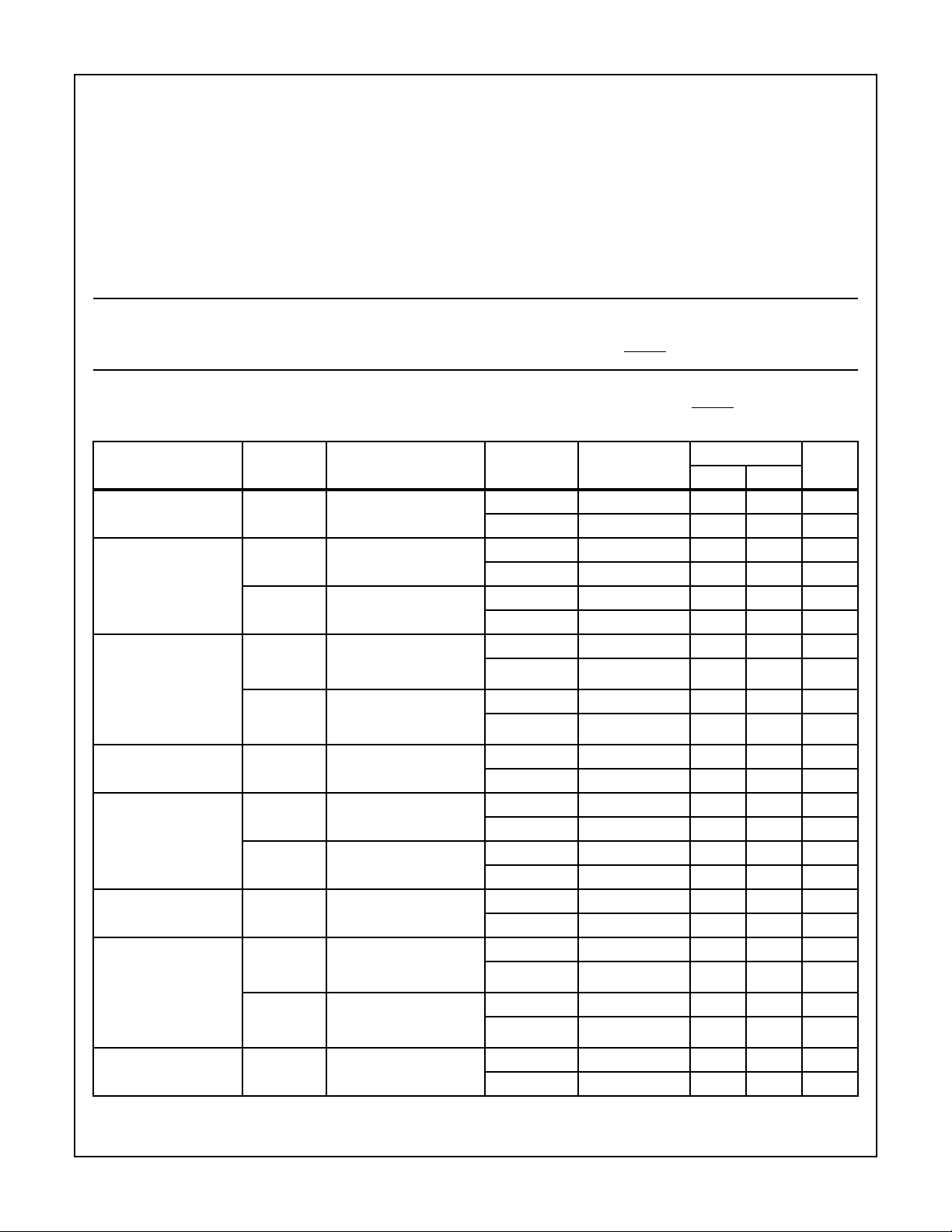
TABLE 1. DC ELECTRICAL PERFORMANCE CHARACTERISTICS
Device Tested at: Supply Voltage = ±15V, R
Unless Otherwise Specified.
SOURCE
= 0Ω, A
VCL
Thermal Package Characteristics θ
CerDIP Package . . . . . . . . . . . . . . . . . . . . . . 115oC/W 30oC/W
Ceramic LCC Package . . . . . . . . . . . . . . . . . 75oC/W 23oC/W
Package Power Dissipation Limit at +75oC for TJ≤ +175oC
CerDIP Package . . . . . . . . . . . . . . . . . . . . . . . . . . . . . . . . . 0.87W
Ceramic LCC Package . . . . . . . . . . . . . . . . . . . . . . . . . . . . 1.33W
Package Power Dissipation Derating Factor Above +75oC
CerDIP Package . . . . . . . . . . . . . . . . . . . . . . . . . . . . . .8.7mW/oC
Ceramic LCC Package . . . . . . . . . . . . . . . . . . . . . . . . 13.3mW/oC
V
≤ 1/2(V+ - V-) RF = 1kΩ
INCM
RL≥ 400Ω V
= +1, RF = 1kΩ, R
LOAD
= 400Ω, V
DISABLE
= 0V, V
OUT
= V+ or 0V
DISABLE
= V+,
JA
θ
JC
PARAMETERS SYMBOL CONDITIONS
Input Offset Voltage V
Common Mode
+CMRR ∆VCM = +10V, V+ = 5V,
Rejection Ratio
IO
VCM = 0V 1 +25oC-88mV
V- = -25V
-CMRR ∆VCM = -10V, V+ = 25V,
V- = -5V
Power Supply Rejection
Ratio
+PSRR ∆V
V+ = 4.5V, V- = -15V;
SUP
= 13.5V,
V+ = 18V, V- = -15V
-PSRR ∆V
SUP
= 13.5V,
V+ = 15V, V- = -4.5V;
V+ = 15V, V- = -18V
Non-Inverting (+IN)
I
BP
VCM = 0V 1 +25oC-88µA
Current
+IN Common Mode
Rejection
IBPCMP ∆VCM = +10V, V+ = 5V,
V- = -25V
IBPCMN ∆VCM = -10V, V+ = 25V,
V- = -5V
Non-Inverting (+IN) Input
+R
Calculated 1/IBPCMP 1 +25oC10-MΩ
IN
Impedance
+IN Power Supply
Rejection
IBPPSP ∆V
V+ = 4.5V, V- = -15V;
SUP
= 13.5V,
V+ = 18V, V- = -15V
IBPPSN ∆V
SUP
= 13.5V,
V+ = 15V, V- = -4.5V;
V+ = 15V, V- = -18V
Inverting Input (-IN)
I
BN
VCM = 0V 1 +25oC -20 20 µA
Current
GROUP A
SUBGROUP TEMPERATURE
LIMITS
UNITSMIN MAX
2, 3 +125oC, -55oC -10 10 mV
1 +25oC60-dB
2, 3 +125oC, -55oC50 - dB
1 +25oC60-dB
2, 3 +125oC, -55oC50 - dB
1 +25oC64-dB
2, 3 +125oC, -55oC60 - dB
1 +25oC64-dB
2, 3 +125oC, -55oC60 - dB
2, 3 +125oC, -55oC -20 20 µA
1 +25oC - 0.1 µA/V
2, 3 +125oC, -55oC - 0.5 µA/V
1 +25oC - 0.1 µA/V
2, 3 +125oC, -55oC - 0.5 µA/V
2, 3 +125oC, -55oC2 - MΩ
1 +25oC - 0.06 µA/V
2, 3 +125oC, -55oC - 0.2 µA/V
1 +25oC - 0.06 µA/V
2, 3 +125oC, -55oC - 0.2 µA/V
2, 3 +125oC, -55oC -50 50 µA
3-95
Spec Number 511080-883
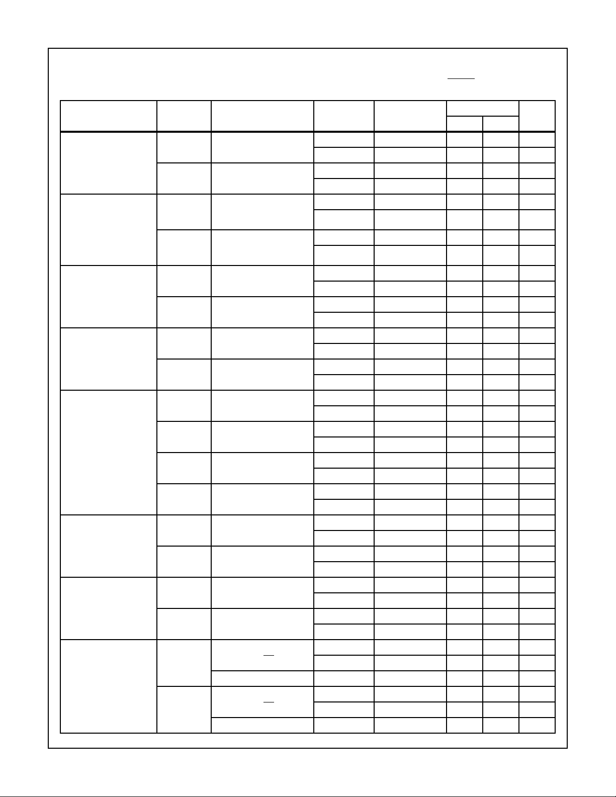
TABLE 1. DC ELECTRICAL PERFORMANCE CHARACTERISTICS (Continued)
Device Tested at: Supply Voltage = ±15V, R
Unless Otherwise Specified.
Specifications HA-5020/883
SOURCE
= 0Ω, A
= +1, RF = 1kΩ, R
VCL
LOAD
= 400Ω, V
OUT
= 0V, V
DISABLE
= V+,
LIMITS
UNITSMIN MAX
PARAMETERS SYMBOL CONDITIONS
-IN Common Mode
Rejection
IBNCMP ∆VCM = +10V, V+ = 5V,
V- = -25V
IBNCMN ∆VCM = -10V, V+ = 25V,
V- = -5V
-IN Power Supply
Rejection
IBNPSP ∆V
V+ = 4.5V, V- = -15V;
SUP
= 13.5V,
V+ = 18V, V- = -15V
IBNPSN ∆V
SUP
= 13.5V,
V+ = 15V, V- = -4.5V;
V+ = 15V, V- = -18V
GROUP A
SUBGROUP TEMPERATURE
1 +25oC - 0.4 µA/V
2, 3 +125oC, -55oC - 0.5 µA/V
1 +25oC - 0.4 µA/V
2, 3 +125oC, -55oC - 0.5 µA/V
1 +25oC - 0.2 µA/V
2, 3 +125oC, -55oC - 0.5 µA/V
1 +25oC - 0.2 µA/V
2, 3 +125oC, -55oC - 0.5 µA/V
Common Mode Range +CMR V+ = 5V, V- = -25V 1 +25oC10-V
2, 3 +125oC, -55oC10 - V
-CMR V+ = 25V, V- = -5V 1 +25oC - -10 V
2, 3 +125oC, -55oC - -10 V
Transimpedance +A
-A
Output Voltage Swing +V
ZOL1
ZOL1
OUT
RL = 400Ω, V
10V
RL = 400Ω, V
-10V
OUT
OUT
= 0 to
= 0 to
1 +25oC1-MΩ
2, 3 +125oC, -55oC1 - MΩ
1 +25oC1-MΩ
2, 3 +125oC, -55oC1 - MΩ
VIN = 12.8V 1, 2 +25oC, +125oC12 - V
3 -55oC11-V
-V
OUT
VIN = -12.8V 1, 2 +25oC, +125oC - -12 V
3 -55oC - -11 V
+V
-V
Output Current +I
OUT5
OUT5
OUT
V+ = 5V, V- = -5V,
VIN = 3V
V+ = 5V, V- = -5V,
VIN = -3V
1 +25oC2-V
2, 3 +125oC, -55oC2 - V
1 +25oC - -2 V
2, 3 +125oC, -55oC - -2 V
Note 1 1, 2 +25oC, +125oC30 - mA
3 -55oC 27.5 - mA
-I
OUT
Note 1 1, 2 +25oC, +125oC - -30 mA
3 -55oC - -27.5 mA
Short Circuit Output
Current
+I
SC
RL = Open, VIN = 10V 1 +25oC50-mA
2, 3 +125oC, -55oC50 - mA
-I
SC
RL = Open, VIN = -10V 1 +25oC - -50 mA
2, 3 +125oC, -55oC - -50 mA
Disabled Output Current +I
LEAK
VIN = 0V, V
RL = Open, V
OUT
DIS
= +10V,
= 0V
1 +25oC-11µA
3 -55oC-11µA
VIN = 2V 2 +125oC-11µA
-I
LEAK
VIN = 0V, V
RL = Open, V
OUT
= -10V,
= 0V
DIS
1 +25oC-11µA
3 -55oC-11µA
VIN = -2V 2 +125oC-11µA
3-96
Spec Number 511080-883
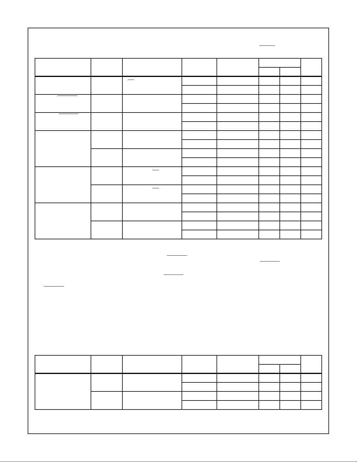
TABLE 1. DC ELECTRICAL PERFORMANCE CHARACTERISTICS (Continued)
Device Tested at: Supply Voltage = ±15V, R
Unless Otherwise Specified.
Specifications HA-5020/883
SOURCE
= 0Ω, A
= +1, RF = 1kΩ, R
VCL
LOAD
= 400Ω, V
OUT
= 0V, V
DISABLE
= V+,
LIMITS
UNITSMIN MAX
PARAMETERS SYMBOL CONDITIONS
Disable Pin Input Current I
LOGIC
V
= 0V 1, 2 +25oC, +125oC-1 0 mA
DIS
GROUP A
SUBGROUP TEMPERATURE
3 -55oC -1.5 0 mA
Minimum DISABLE Pin
Current to Disable
Maximum DISABLE Pin
Current to Enable
Quiescent Power Supply
Current
I
DIS
Note 2 1 +25oC - 350 µA
2, 3 +125oC, -55oC - 350 µA
I
EN
Note 3 1 +25oC20-µA
2, 3 +125oC, -55oC20 - µA
I
CC
RL = 400Ω 1 +25oC - 10 mA
2, 3 +125oC, -55oC - 10 mA
I
EE
RL = 400Ω 1 +25oC -10 - mA
2, 3 +125oC, -55oC -10 - mA
Disabled Power Supply
Current
I
CCDIS
I
EEDIS
RL = 400Ω, V
RL = 400Ω, V
= 0V 1 +25oC - 5.6 mA
DIS
2, 3 +125oC, -55oC - 7.5 mA
= 0V 1 +25oC -5.6 - mA
DIS
2, 3 +125oC, -55oC -7.5 - mA
Offset Voltage
Adjustment
+V
-V
ADJ
ADJ
Note 4 1 +25oC30-mV
2, 3 +125oC, -55oC25 - mV
Note 4 1 +25oC - -30 mV
2, 3 +125oC, -55oC - -25 mV
NOTES:
1. Guaranteed from V
OUT
test by I
OUT
= V
OUT
/400Ω.
2. This is the minimum current which must be sourced from the DISABLE pin, to disable the output. The output is considered disabled when
V
≤ 10mV. Conditions are: VIN = 10V, RL = 100Ω. The test is performed by sourcing 350µA from the DISABLE pin, and testing that
OUT
the output decreases below the test limit (10mV).
3. This is the maximum current that can be sourced from the DISABLE pin with the device remaining enabled. The device is considered
disabled when the supply current decreases by at least 0.5mA. Conditions are: RL = 400Ω. Test is performed by sourcing 20µA from the
DISABLE pin, and testing that the supply current decreases by no more than the test limit (0.5mA).
4. The offset adjustment range is referred to the output. The inv erting input current (-I
1 and 5, wiper connected to V+. Since -I
flows through RF, an adjustment of offset voltage results. The amount of offset adjustment is
BIAS
proportional to the value of RF. Test conditions are: RL = Open, 10kΩ from pin 5 to V+, 1kΩ from pin 1 to V+, for +V
from pin 5 to V+, 10kΩ from pin 1 to V+, for -V
ADJ
.
) can be adjusted with an external pot between pins
BIAS
; RL = Open, 1kΩ
ADJ
TABLE 2. AC ELECTRICAL PERFORMANCE CHARACTERISTICS
Device Tested at: Supply Voltage = ±15V, R
PARAMETERS SYMBOL CONDITIONS
SOURCE
= 50Ω, R
LOAD
= 400Ω, C
LOAD
≤ 10pF, A
GROUP A
SUBGROUP TEMPERATURE
= +1V/V, Unless Otherwise Specified.
VCL
LIMITS
UNITSMIN MAX
Slew Rate +SR VIN= -10V to +10V 4 +25oC 600 - V/µs
5, 6 +125oC, -55oC 400 - V/µs
-SR VIN= +10V to -10V 4 +25oC 600 - V/µs
5, 6 +125oC, -55oC 400 - V/µs
Spec Number 511080-883
3-97
Specifications HA-5020/883
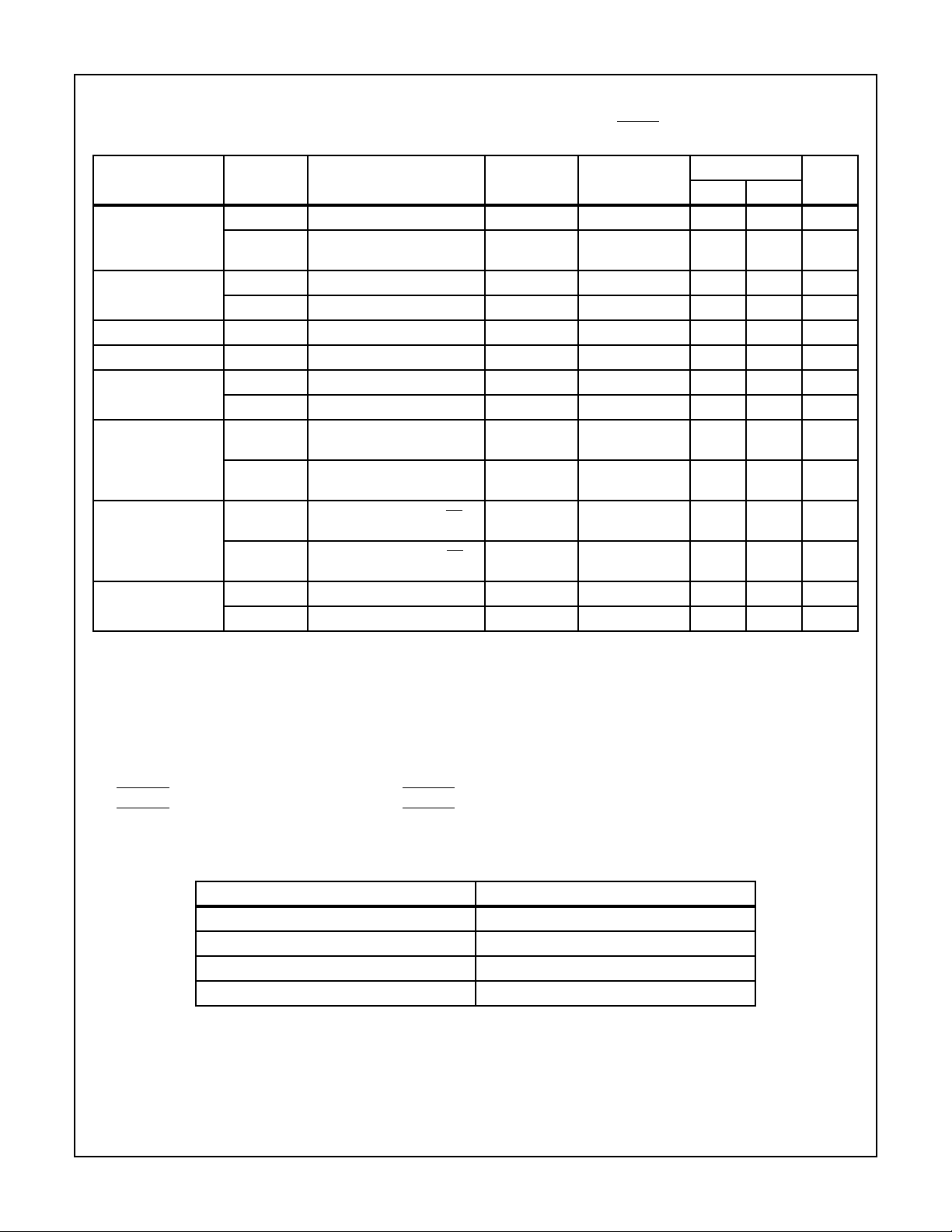
TABLE 3. ELECTRICAL PERFORMANCE CHARACTERISTICS
Device Characterized at: Supply Voltage = ±15V, R
Unless Otherwise Specified.
PARAMETERS SYMBOL CONDITIONS NOTES TEMPERATURE
-3dB Bandwidth BW
BW
1
10
VO = 100mV
VO = 100mV
RF = 360Ω, RL = Open
Gain Flatness GF
GF
Rise Time t
Fall Time t
R
F
VO = 100mV
5
VO = 100mV
10
VO = 0V to 1V, RL = 100Ω 1, 2 +25oC - 3.7 ns
VO = 1V to 0V, RL = 100Ω 1, 3 +25oC - 4.0 ns
Overshoot +OVS VO = 0V to 1V, RL = 100Ω 1 +25oC - 18.0 %
-OVS VO = 1V to 0V, RL = 100Ω 1 +25oC - 16.6 %
Slew Rate +SR
VO = -10V to 10V, AV = +10,
10
RF = 360Ω, RL = Open
-SR
VO = 10V to -10V, AV = +10,
10
RF = 360Ω, RL = Open
Disable Time +t
Enable Time +t
DIS
-t
DIS
EN
-t
EN
VO = 2V to 0V, 50% of V
90% V
O
VO = -2V to 0V, 50% of V
90% V
O
VO = 0V to 2V, 50% to 90% 1, 7 +25oC - 1.45 µs
VO = 0V to -2V, 50% to 90% 1, 7 +25oC - 1.49 µs
NOTES:
1. Parameters listed in Table 3 are controlled via design or process parameters and are not directly tested at final production. These param-
eters are lab characterized upon initial design release, or upon design changes. These parameters are guaranteed by characterization
based upon data from multiple production runs which reflect lot to lot and within lot variation.
2. Measured from 10% to 90% of the output waveform.
3. Measured from 90% to 10% of the output waveform.
4. Measured from 25% to 75% of the output waveform.
5. Measured from 75% to 25% of the output waveform.
6. DISABLE = +15V to 0V. Measured from the 50% of DISABLE to V
7. DISABLE = 0V to +15V. Measured from the 50% of DISABLE to V
SOURCE
= 50Ω, R
= 400Ω, RF = 1kΩ, V
LOAD
DISABLE
= V+, C
LOAD
≤ 10pF, A
LIMITS
, AV = +1 1 +25oC 105 - MHz
RMS
, AV = +10,
RMS
, f = 5MHz 1 +25oC -0.075 +0.075 dB
RMS
, f = 10MHz 1 +25oC -0.2 +0.2 dB
RMS
1 +25oC 77 - MHz
1, 4 +25oC 1070 - V/µs
1, 5 +25oC 860 - V/µs
DIS
DIS
to
to
1, 6 +25oC - 3.13 µs
1, 6 +25oC - 2.44 µs
= ±200mV.
OUT
= ±1.8V.
OUT
VCL
= +1V/V,
UNITSMIN MAX
TABLE 4. ELECTRICAL TEST REQUIREMENTS
MIL-STD-883 TEST REQUIREMENTS SUBGROUPS (SEE TABLES 1 AND 2)
Interim Electrical Parameters (Pre Burn-In) 1
Final Electrical Test Parameters 1 (Note 1), 2, 3, 4, 5, 6
Group A Test Requirements 1, 2, 3, 4, 5, 6
Groups C and D Endpoints 1
NOTE:
1. PDA applies to Subgroup 1 only.
3-98
Spec Number 511080-883
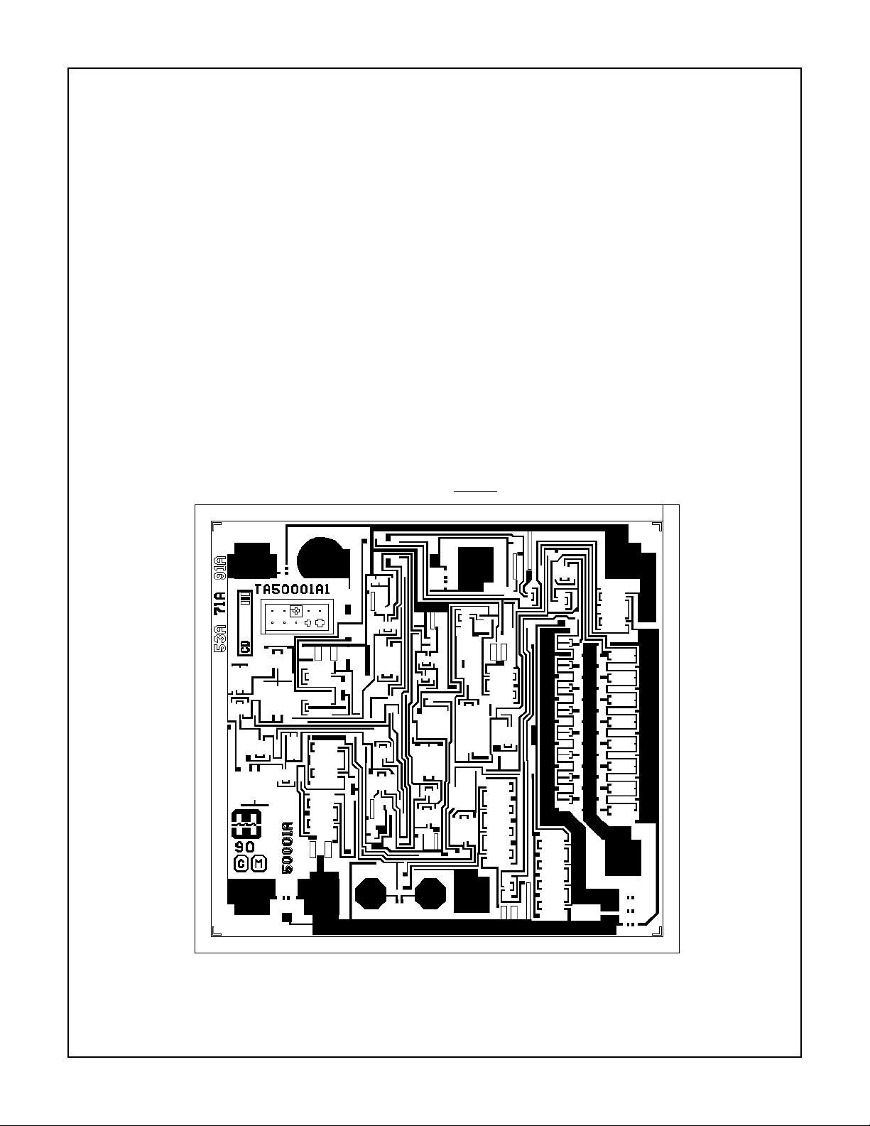
Die Characteristics
DIE DIMENSIONS:
65 x 60 x 19 mils ± 1 mils
1640µm x 1520µm x 483µm ± 25.4µm
METALLIZATION:
Type: Al, 1% Cu
Thickness: 16k
WORST CASE CURRENT DENSITY:
5.77 x 10
Å ± 2kÅ
4
A/cm2 at 30mA
SUBSTRATE POTENTIAL (Powered Up): V-
GLASSIVATION:
Type: Nitride over Silox
Silox Thickness: 12k
Å ± 2kÅ
Nitride Thickness: 3.5kÅ ± 1kÅ
TRANSISTOR COUNT: 62
PROCESS: Bipolar Dielectric Isolation
Metallization Mask Layout
HA-5020/883
HA-5020/883
-IN
+IN
BAL DISABLE V+
21 8 7
6
43
5
OUT
3-99
BALV-
Spec Number 511080-883
 Loading...