intersil HA-5020 DATA SHEET
®
HA-5020
Data Sheet June 5, 2006 FN2845.11
100MHz Current Feedback
Video Amplifier With Disable
The HA-5020 is a wide bandwidth, high slew rate amplifier
optimized for video applications and gains between 1 and
10. Manufactured on Intersil’s Reduced Feature
Complementary Bipolar DI process, this amplifier uses
current mode feedback to maintain higher bandwidth at a
given gain than conventional voltage feedback amplifiers.
Since it is a closed loop device, the HA-5020 offers better
gain accuracy and lower distortion than open loop buffers.
The HA-5020 features low differential gain and phase and
will drive two double terminated 75Ω coax cables to video
levels with low distortion. Adding a gain flatness
performance of 0.1dB makes this amplifier ideal for
demanding video applications. The bandwidth and slew rate
of the HA-5020 are relatively independent of closed loop
gain. The 100MHz unity gain bandwidth only decreases to
60MHz at a gain of 10. The HA-5020 used in place of a
conventional op amp will yield a significant improvement in
the speed power product. T o further reduce power, HA-5020
has a disable function which significantly reduces supply
current, while forcing the output to a true high impedance
state. This allows the outputs of multiple amplifiers to be
wire-OR’d into multiplexer configurations. The device also
includes output short circuit protection and output offset
voltage adjustment.
For multi channel versions of the HA-5020 see the HA5022
dual with disable, HA5023 dual, HA5013 triple and HA5024
quad with disable op amp data sheets.
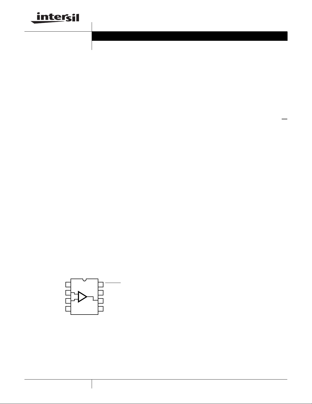
Pinout
HA-5020
(PDIP, SOIC)
TOP VIEW
Features
• Wide Unity Gain Bandwidth . . . . . . . . . . . . . . . . . 100MHz
• Slew Rate. . . . . . . . . . . . . . . . . . . . . . . . . . . . . . . 800V/µs
• Output Current . . . . . . . . . . . . . . . . . . . . . . . ±30mA (Min)
• Drives 3.5V into 75Ω
• Differential Gain . . . . . . . . . . . . . . . . . . . . . . . . . . . 0.03%
• Differential Phase. . . . . . . . . . . . . . . . . . . . . . . . . . . .0.03°
• Low Input Voltage Noise . . . . . . . . . . . . . . . . . 4.5nV/√Hz
• Low Supply Current . . . . . . . . . . . . . . . . . . . . 10mA (Max)
• Wide Supply Range . . . . . . . . . . . . . . . . . . . ±5V to ±15V
• Output Enable/Disable
• High Performance Replacement for EL2020
• Pb-Free Plus Anneal Available (RoHS Compliant)
Applications
• Unity Gain Video/Wideband Buffer
• Video Gain Block
• Video Distribution Amp/Coax Cable Driver
• Flash A/D Driver
• Waveform Generator Output Driver
• Current to Voltage Converter; D/A Output Buffer
• Radar Systems
• Imaging Systems
BAL
IN-
IN+
1
2
-
+
3
4
V-
8
DISABLE
7
V+
6
OUT
5
BAL
1
CAUTION: These devices are sensitive to electrostatic discharge; follow proper IC Handling Procedures.
1-888-INTERSIL or 1-888-468-3774
| Intersil (and design) is a registered trademark of Intersil Americas Inc.
Copyright Intersil Americas Inc. 2002, 2005-2006. All Rights Reserved
All other trademarks mentioned are the property of their respective owners.
HA-5020
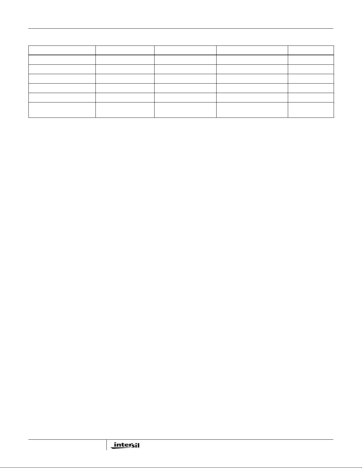
Ordering Information
PART NUMBER PART MARKING TEMP. RANGE (°C) PACKAGE PKG. DWG. #
HA3-5020-5 HA3-5020-5 0 to 75 8 Ld PDIP E8.3
HA3-5020-5Z (Note) HA3-5020-5Z 0 to 75 8 Ld PDIP (Pb-free) E8.3
HA9P5020-5 50205 0 to 75 8 Ld SOIC M8.15
HA9P5020-5Z (Note) 50205Z 0 to 75 8 Ld SOIC (Pb-free) M8.15
HA9P5020-5X96 50205 0 to 75 8 Ld SOIC Tape and Reel M8.15
HA9P5020-5ZX96 (Note) 50205Z 0 to 75 8 Ld SOIC Tape and Reel
(Pb-free)
NOTE: Intersil Pb-free plus anneal products employ special Pb-free material sets; molding compounds/die attach materials and 100% matte tin plate
termination finish, which are RoHS compliant and compatible with both SnPb and Pb-free soldering operations. Intersil Pb-free products are MSL
classified at Pb-free peak reflow temperatures that meet or exceed the Pb-free requirements of IPC/JEDEC J STD-020.
M8.15
2
FN2845.11
June 5, 2006
HA-5020
Absolute Maximum Ratings (Note 1) Thermal Information
Voltage Between V+ and V- Terminals . . . . . . . . . . . . . . . . . . . 36V
DC Input Voltage . . . . . . . . . . . . . . . . . . . . . . . . . . . . . . . ±V
Differential Input Voltage . . . . . . . . . . . . . . . . . . . . . . . . . . . . . . 10V
SUPPLY
Output Current . . . . . . . . . . . . . . . . . . . . . . . Short Circuit Protected
Operating Conditions
Temperature Range
HA-5020-5 . . . . . . . . . . . . . . . . . . . . . . . . . . . . . . . . . . . 0°C to 75°C
CAUTION: Stresses above those listed in “Absolute Maximum Ratings” may cause permanent damage to the device. This is a stress only rating and operation of the
device at these or any other conditions above those indicated in the operational sections of this specification is not implied.
NOTES:
1. Maximum power dissipation, including output load, must be designed to maintain junction temperature below 150°C for plastic packages.
is measured with the component mounted on a low effective thermal conductivity test board in free air. See Tech Brief TB379 for details.
1. θ
JA
Thermal Resistance (Typical, Note 2) θ
PDIP Package . . . . . . . . . . . . . . . . . . . 120 N/A
(°C/W) θJC (°C/W)
JA
SOIC Package . . . . . . . . . . . . . . . . . . . 165 N/A
Maximum Junction Temperature (Plastic Packages, Note 1) . . . 150°C
Maximum Storage Temperature Range . . . . . . . . . -65°C to 150°C
Maximum Lead Temperature (Soldering 10s) . . . . . . . . . . . . 300°C
(SOIC - Lead Tips Only)
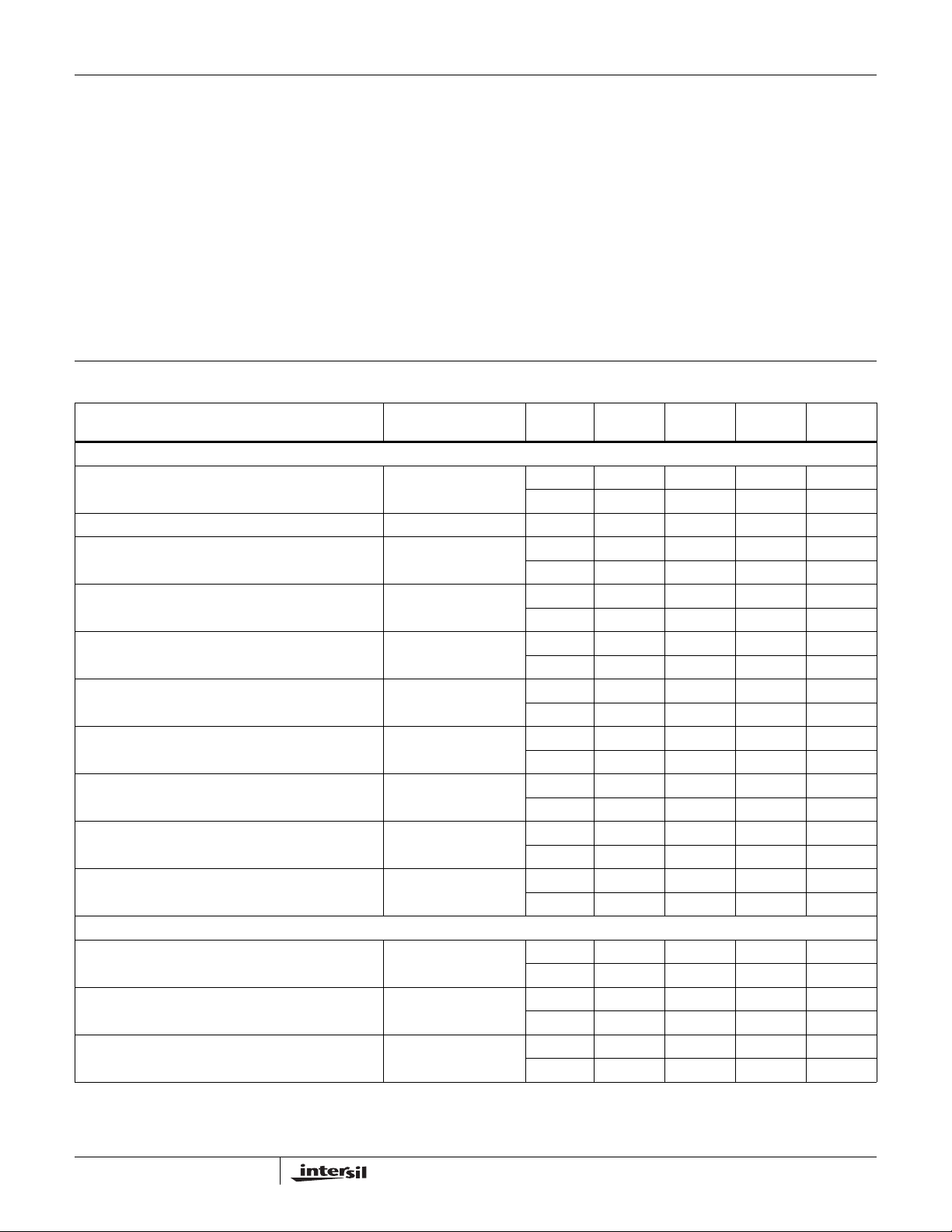
Electrical Specifications V
Unless Otherwise Specified
= ±15V, RF = 1kΩ, AV = +1, RL = 400Ω, CL ≤ 10pF,
SUPPLY
TEMP.
PARAMETER TEST CONDITIONS
(°C) MIN TYP MAX UNITS
INPUT CHARACTERISTICS
Input Offset Voltage (Notes 3, 14) 25 - 2 8 mV
Full - - 10 mV
Average Input Offset Voltage Drift Full - 10 - µV/°C
Common Mode Rejection Ratio (Note 14) VCM = ±10V 25 60 - - dB
V
IO
Full 50 - - dB
Power Supply Rejection Ratio (Note 14) ±4.5V ≤ VS ≤ ±18V 25 64 - - dB
V
IO
Full 60 - - dB
Non-Inverting Input (+IN) Current (Note 14) 25 - 3 8 µA
Full - - 20 µA
+IN Common Mode Rejection V
= ±10V 25 - - 0.1 µA/V
CM
Full - - 0.5 µA/V
+IN Power Supply Rejection ±4.5V ≤ V
≤ ±18V 25 - - 0.06 µA/V
S
Full - - 0.2 µA/V
Inverting Input (-IN) Current (Note 14) 25 - 12 20 µA
Full - 25 50 µA
-IN Common Mode Rejection V
= ±10V 25 - - 0.4 µA/V
CM
Full - - 0.5 µA/V
-IN Power Supply Rejection ±4.5V ≤ V
≤ ±18V 25 - - 0.2 µA/V
S
Full - - 0.5 µA/V
TRANSFER CHARACTERISTICS
Transimpedance (Notes 9, 14) 25 3500 - - V/mA
Full 1000 - - V/mA
Open Loop DC Voltage Gain (Note 9) R
Open Loop DC Voltage Gain R
= 400Ω,
L
V
OUT
= 100Ω,
L
V
OUT
= ±10V
= ±2.5V
25 70 - - dB
Full 65 - - dB
25 60 - - dB
Full 55 - - dB
3
FN2845.11
June 5, 2006

HA-5020
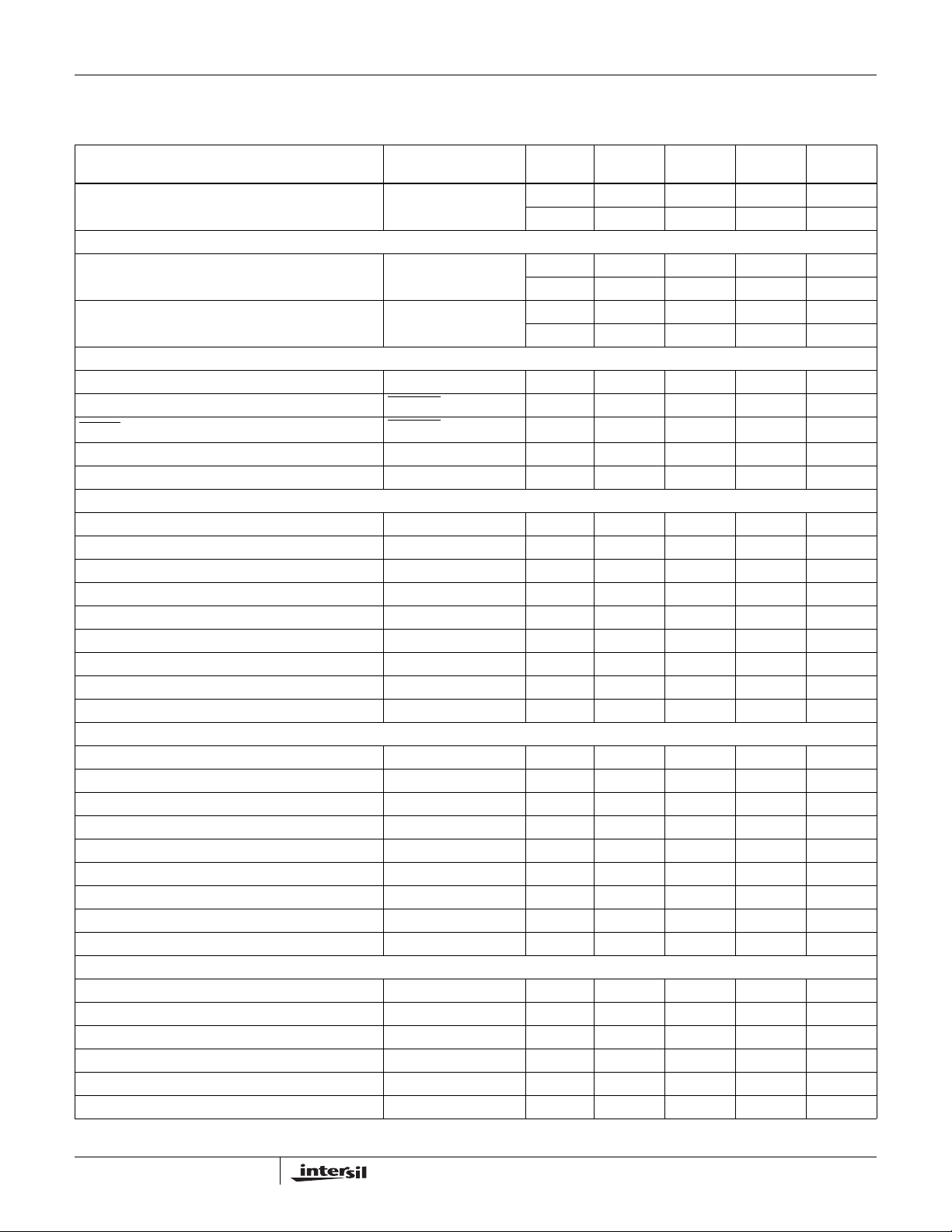
Electrical Specifications V
Unless Otherwise Specified
PARAMETER TEST CONDITIONS
OUTPUT CHARACTERISTICS
Output Voltage Swing (Note 14) R
Output Current (Guaranteed by Output Voltage Test) 25 ±30 ±31.7 - mA
POWER SUPPLY CHARACTERISTICS
Quiescent Supply Current (Note 14) Full - 7.5 10 mA
Supply Current, Disabled (Note 14) DISABLE
Pin Input Current DISABLE = 0V Full - 1.0 1.5 mA
Disable
Minimum Pin 8 Current to Disable (Note 4) Full 350 - - µA
Maximum Pin 8 Current to Enable (Note 5) Full - - 20 µA
AC CHARACTERISTICS (A
Slew Rate (Note 6) 25 600 800 - V/µs
Full Power Bandwidth (Note 7)
(Guaranteed by Slew Rate Test)
Rise Time (Note 8) 25 - 5 - ns
Fall Time (Note 8) 25 - 5 - ns
Propagation Delay (Notes 8, 14) 25 - 6 - ns
-3dB Bandwidth (Note 14) V
Settling Time to 1% 10V Output Step 25 - 45 - ns
Settling Time to 0.25% 10V Output Step 25 - 100 - ns
AC CHARACTERISTICS (A
Slew Rate (Notes 6, 9) 25 900 1100 - V/µs
Full Power Bandwidth (Note 7)
(Guaranteed by Slew Rate Test)
Rise Time (Note 8) 25 - 8 - ns
Fall Time (Note 8) 25 - 8 - ns
Propagation Delay (Notes 8, 14) 25 - 9 - ns
-3dB Bandwidth V
Settling Time to 1% 10V Output Step 25 - 55 - ns
Settling Time to 0.1% 10V Output Step 25 - 90 - ns
INTERSIL VALUE ADDED SPECIFICATIONS
Input Noise Voltage (Note 14) f = 1kHz 25 - 4.5 - nV/√Hz
+Input Noise Current (Note 14) f = 1kHz 25 - 2.5 - pA/√Hz
-Input Noise Current (Note 14) f = 1kHz 25 - 25 - pA/√Hz
Input Common Mode Range Full ±10 ±12 - V
-I
Adjust Range (Note 3) Full ±25 ±40 - µA
BIAS
Overshoot (Note 14) 25 - 7 - %
= +1)
V
= +10, RF = 383Ω)
V
= ±15V, RF = 1kΩ, AV = +1, RL = 400Ω, CL ≤ 10pF,
SUPPLY
(Continued)
= 150Ω 25 to 85 ±12 ±12.7 - V
L
= 0V Full - 5 7.5 mA
= 100mV 25 - 100 - MHz
OUT
= 100mV 25 - 6 0 - MHz
OUT
TEMP.
(°C) MIN TYP MAX UNITS
-40 to 0 ±11 ±11.8 - V
Full ±27.5 - - mA
Full 500 700 - V/µs
25 9.6 12.7 - MHz
Full 8.0 11.1 - MHz
Full 700 - - V/µs
25 14.3 17.5 - MHz
Full 11.1 - - MHz
4
FN2845.11
June 5, 2006

HA-5020
Electrical Specifications V
Unless Otherwise Specified
PARAMETER TEST CONDITIONS
Output Current, Short Circuit (Note 14) VIN = ±10V, V
Output Current, Disabled (Note 14) DISABLE
Output Disable Time (Notes 10, 14) 25 - 10 - µs
Output Enable Time (Notes 11, 14) 25 - 200 - ns
Supply Voltage Range 25 ±5-±15 V
Output Capacitance, Disabled (Note 12) DISABLE
VIDEO CHARACTERISTICS
Differential Gain (Notes 13, 14) R
Differential Phase (Notes 13, 14) R
Gain Flatness To 5MHz 25 - 0.1 - dB
Electrical Specifications V+ = +5V, V- = -5V, R
Parameters are not tested. The limits are guaranteed based on lab characterizations, and reflect
lot-to-lot variation.
PARAMETER TEST CONDITIONS
INPUT CHARACTERISTICS
Input Offset Voltage (Notes 3, 14) 25 - 2 8 mV
Average Input Offset Voltage Drift Full - 10 - µV/°C
Common Mode Rejection Ratio (Notes 14, 15) 25 50 - - dB
V
IO
Power Supply Rejection Ratio (Note 14) ±3.5V ≤ VS ≤ ±6.5V 25 55 - - dB
V
IO
Non-Inverting Input (+IN) Current (Note 14) 25 - 3 8 µA
+IN Common Mode Rejection (Note 15) 25 - - 0.1 µA/V
+IN Power Supply Rejection ±3.5V ≤ V
Inverting Input (-IN) Current (Note 14) 25 - 12 20 µA
-IN Common Mode Rejection (Note 15) 25 - - 0.4 µA/V
-IN Power Supply Rejection ±3.5V ≤ V
TRANSFER CHARACTERISTICS
Transimpedance (Notes 9, 14) 25 1000 - - V/mA
Open Loop DC Voltage Gain R
= ±15V, RF = 1kΩ, AV = +1, RL = 400Ω, CL ≤ 10pF,
SUPPLY
(Continued)
= 0V Full ±50 ±65 - mA
OUT
= 0V,
V
= ±10V
OUT
= 0V 25 - 6 - pF
= 150Ω 25 - 0.03 - %
L
= 150Ω 25 - 0.03 - °
L
= 1kΩ, AV = +1, RL = 400Ω, CL ≤10pF, Unless Otherwise Specified.
F
≤ ±6.5V 25 - - 0.06 µA/V
S
≤ ±6.5V 25 - - 0.2 µA/V
S
= 400Ω,
L
V
= ±2.5V
OUT
TEMP.
(°C) MIN TYP MAX UNITS
Full - - 1 µA
TEMP.
(°C) MIN TYP MAX UNITS
Full - - 10 mV
Full 35 - - dB
Full 50 - - dB
Full - - 20 µA
Full - - 0.5 µA/V
Full - - 0.2 µA/V
Full - 25 50 µA
Full - - 0.5 µA/V
Full - - 0.5 µA/V
Full 850 - - V/mA
25 65 - - dB
Full 60 - - dB
5
FN2845.11
June 5, 2006
HA-5020
Electrical Specifications V+ = +5V, V- = -5V, R
= 1kΩ, AV = +1, RL = 400Ω, CL ≤10pF, Unless Otherwise Specified.
F
Parameters are not tested. The limits are guaranteed based on lab characterizations, and reflect
lot-to-lot variation.
(Continued)
TEMP.
PARAMETER TEST CONDITIONS
Open Loop DC Voltage Gain RL = 100Ω,
V
= ±2.5V
OUT
(°C) MIN TYP MAX UNITS
25 50 - - dB
Full 45 - - dB
OUTPUT CHARACTERISTICS
Output Voltage Swing (Note 14) 25 to 85 ±2.5 ±3.0 - V
-40 to 0 ±2.5 ±3.0 - V
Output Current
(Guaranteed by Output Voltage Test)
= 100Ω 25 ±16.6 ±20 - mA
R
L
Full ±16.6 ±20 - mA
POWER SUPPLY CHARACTERISTICS
Quiescent Supply Current (Note 14) Full - 7.5 10 mA
Supply Current, Disabled (Note 14) DISABLE
Pin Input Current
Disable
DISABLE
= 0V Full - 5 7.5 mA
= 0V Full - 1.0 1.5 mA
Minimum Pin 8 Current to Disable (Note 16) Full 350 - - µA
Maximum Pin 8 Current to Enable (Note 5) Full - - 20 µA
AC CHARACTERISTICS (A
= +1)
V
Slew Rate (Note 17) 25 215 400 - V/µs
Full Power Bandwidth (Note 18) 25 22 28 - MHz
Rise Time (Note 8) 25 - 6 - ns
Fall Time (Note 8) 25 - 6 - ns
Propagation Delay (Note 8) 25 - 6 - ns
Overshoot 25 - 4.5 - %
-3dB Bandwidth (Note 14) V
= 100mV 25 - 125 - MHz
OUT
Settling Time to 1% 2V Output Step 25 - 50 - ns
Settling Time to 0.25% 2V Output Step 25 - 75 - ns
AC CHARACTERISTICS (A
= +2, RF = 681Ω)
V
Slew Rate (Note 17) 25 - 475 - V/µs
Full Power Bandwidth (Note 18) 25 - 26 - MHz
Rise Time (Note 8) 25 - 6 - ns
Fall Time (Note 8) 25 - 6 - ns
Propagation Delay (Note 8) 25 - 6 - ns
Overshoot 25 - 12 - %
-3dB Bandwidth (Note 14) V
= 100mV 25 - 9 5 - MHz
OUT
Settling Time to 1% 2V Output Step 25 - 50 - ns
Settling Time to 0.25% 2V Output Step 25 - 100 - ns
AC CHARACTERISTICS (A
= +10, RF = 383Ω)
V
Slew Rate (Note 17) 25 350 475 - V/µs
Full Power Bandwidth (Note 18) 25 28 38 - MHz
Rise Time (Note 8) 25 - 8 - ns
Fall Time (Note 8) 25 - 9 - ns
Propagation Delay (Note 8) 25 - 9 - ns
Overshoot 25 - 1.8 - %
6
FN2845.11
June 5, 2006
HA-5020
Electrical Specifications V+ = +5V, V- = -5V, R
= 1kΩ, AV = +1, RL = 400Ω, CL ≤10pF, Unless Otherwise Specified.
F
Parameters are not tested. The limits are guaranteed based on lab characterizations, and reflect
lot-to-lot variation.
(Continued)
TEMP.
PARAMETER TEST CONDITIONS
-3dB Bandwidth (Note 14) V
= 100mV 25 - 6 5 - MHz
OUT
(°C) MIN TYP MAX UNITS
Settling Time to 1% 2V Output Step 25 - 75 - ns
Settling Time to 0.25% 2V Output Step 25 - 130 - ns
INTERSIL VALUE ADDED SPECIFICATIONS
Input Noise Voltage (Note 14) f = 1kHz 25 - 4.5 - nV/√Hz
+Input Noise Current (Note 14) f = 1kHz 25 - 2.5 - pA/√Hz
-Input Noise Current (Note 14) f = 1kHz 25 - 25 - pA/√Hz
Input Common Mode Range Full ±2.5V − -V
Output Current, Short Circuit V
= ±2.5V, V
IN
Output Current, Disabled (Note 14) DISABLE
V
= ±2.5V , VIN = 0V
OUT
= 0V ,
= 0V Full ±40 ±60 - mA
OUT
Full - - 2 µA
Output Disable Time (Notes 14, 20) 25 - 40 - µs
Output Enable Time (Notes 14, 21) 25 - 40 - ns
Supply Voltage Range 25 ±5-±15 V
Output Capacitance, Disabled (Note 19) DISABLE
= 0V 25 - 6 - pF
VIDEO CHARACTERISTICS
Differential Gain (Notes 13, 14) R
Differential Phase (Notes 13, 14) R
= 150Ω 25 - 0.03 - %
L
= 150Ω 25 - 0.03 - °
L
Gain Flatness To 5MHz 25 - 0.1 - dB
NOTES:
2. Suggested V
connected to V+. Since -I
adjustment is determined by the value of R
3. R
= 100Ω, VIN = 10V . This is the minimum current which must be pulled out of the Disable pin in order to disable the output. The output is
L
considered disabled when -10mV ≤ V
4. V
= 0V . This is the maximum current that can be pulled out of the Disable pin with the HA-5020 remaining enabled. The HA-5020 is considered
IN
Adjust Circuit: The inverting input current (-I
OS
flows through the feedback resistor (RF), the result is an adjustment in offset voltage. The amount of offset voltage
BIAS
OUT
(∆VOS = ∆-I
F
≤ +10mV.
) can be adjusted with an external 10kΩ pot between pins 1 and 5, wiper
BIAS
).
BIAS*RF
disabled when the supply current has decreased by at least 0.5mA.
5. V
6.
7. R
switches from -10V to +10V, or from +10V to -10V. Specification is from the 25% to 75% points.
OUT
Slew Rate
FPBW
= 100Ω, V
L
---------------------------
2π V
OUT
;V
PEAK
= 1V. Measured from 10% to 90% points for rise/fall times; from 50% points of input and output for propagation delay.
PEAK
= 10V.=
8. This parameter is not tested. The limits are guaranteed based on lab characterization, and reflect lot-to-lot variation.
9. V
= +10V, Disable = +15V to 0V. Measured from the 50% point of Disable to V
IN
10. V
= +10V, Disable = 0V to +15V. Measured from the 50% point of Disable to V
IN
11. V
= 0V, Force V
IN
from 0V to ±10V, tR = tF = 50ns.
OUT
OUT
OUT
= 0V.
= 10V.
12. Measured with a VM700A video tester using a NTC-7 composite VITS.
13. See “Typical Performance Curves” for more information.
14. V
15. R
16. V
17. FPBW = .
18. V
19. V
20. V
= ±2.5V. At -40°C product is tested at VCM = ±2.25V because short test duration does not allow self heating.
CM
= 100Ω. VIN = 2.5V . This is the minimum current which must be pulled out of the Disable pin in order to disable the output. The output is
L
considered disabled when -10mV ≤ V
switches from -2V to +2V, or from +2V to -2V. Specification is from the 25% to 75% points.
OUT
Slew Rate
---------------------------
2π V
= 0V, Force V
IN
= +2V, Disable = +5V to 0V. Measured from the 50% point of Disable to V
IN
= +2V, Disable = 0V to +5V. Measured from the 50% point of Disable to V
IN
;V
PEAK
OUT
=2V
PEAK
from 0V to ±2.5V, tR = tF = 50ns.
OUT
≤ +10mV.
OUT
OUT
= 0V.
= 2V.
7
FN2845.11
June 5, 2006
