®
www.BDTIC.com/Intersil
HA-5002/883
Data Sheet January 5, 2006
Monolithic, Wideband, High Slew Rate,
High Output Current Buffer
The HA-5002/883 is a monolithic, wideband, high slew rate,
high output current, buffer amplifier.
Utilizing the advantages of the Intersil Dielectric Isolation
technologies, the HA-5002/883 current buffer offers
1300V/µs slew rate typically and 1000V/µs minimum with
110MHz of bandwidth. The ±100mA minimum output current
capability is enhanced by a 3Ω output impedance.
The monolithic HA-5002/883 will replace the hybrid LH0002
with corresponding performance increases. These
characteristics range from the 3MΩ (typ) input impedance to
the increased output voltage swing. Monolithic design
technologies have allowed a more precise buffer to be
developed with more than an order of magnitude smaller
gain error. The voltage gain is 0.98 guaranteed minimum
with a 1kΩ load and 0.96 minimum with a 100Ω load.
The HA-5002/883 will provide many present hybrid users
with a higher degree of reliability and at the same time
increase overall circuit performance.
Ordering Information
PART
NUMBER
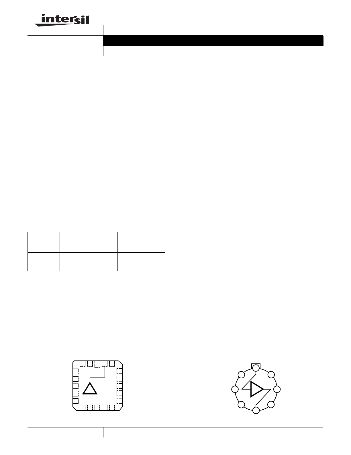
HA2-5002/883 HA2-5002/883 -55 to +125 8 Pin Can
HA4-5002/883 HA4-5002/883 -55 to +125 20 Ld Ceramic LCC
PAR T
MARKING
TEMP
RANGE
(°C) PACKAGE
FN3705.4
Features
• This Circuit is Processed in Accordance to MIL-STD-883
and is Fully Conformant Under the Provisions of
Paragraph 1.2.1.
• Voltage Gain (R
= 1kΩ) . . . . . . . . . . . . . . . . . . 0.98 (Min)
L
0.995 (Typ)
= 100Ω) . . . . . . . . . . . . . . . . .0.96 (Min)
(R
L
0.971 (Typ)
• High Input Impedance . . . . . . . . . . . . . . . . . . 1.5MΩ (Min)
3MΩ (Typ)
• Low Output Impedance . . . . . . . . . . . . . . . . . . . 5Ω (Max)
3Ω (Typ)
• Very High Slew Rate . . . . . . . . . . . . . . . . .1000V/µs (Min)
1300V/µs (Typ)
• Wide Small Signal Bandwidth . . . . . . . . . . .110MHz (Typ)
• High Output Current . . . . . . . . . . . . . . . . . . . .100mA (Min)
• High Pulsed Output Current . . . . . . . . . . . . . 400mA (Max)
• Monolithic Dielectric Isolation Construction
• Replaces Hybrid LH0002
Applications
• Line Driver
• Data Acquisition
• 110MHz Buffer
• High Power Current Booster
• High Power Current Source
• Sample and Holds
• Radar Cable Driver
• Video Products
Pinouts
HA-5002/883 (CLCC)
TOP VIEW
+
1
NCNCNC
V
OUT
3 2 1 20 19
18
NC
V
NC
NC
NC
4
-
5
2
6
7
8
9101112
NC
-
IN
NC
V
1
1
NC
V2+
17
16
NC
NC
15
NC
14
13
NC
CAUTION: These devices are sensitive to electrostatic discharge; follow proper IC Handling Procedures.
1-888-INTERSIL or 1-888-468-3774
| Intersil (and design) is a registered trademark of Intersil Americas Inc.
Copyright Intersil Americas Inc. 2002, 2004-2006. All Rights Reserved
All other trademarks mentioned are the property of their respective owners.
HA-5002/883
(METAL CAN)
TOP VIEW
IN
8
V
+
1
1
2
3
NC NC
4
OUT
V
7
6
5
-
1
V2-V2+

HA-5002/883
www.BDTIC.com/Intersil
Absolute Maximum Ratings Thermal Information
Voltage Between V+ and V- Terminals. . . . . . . . . . . . . . . . . . . . .44V
Input Voltage . . . . . . . . . . . . . . . . . . . . . . . . . . . . . Equal to Supplies
Peak Output Current (50ms On, 1s Off) . . . . . . . . . . . . . . . . . .±400mA
Junction Temperature (T
) . . . . . . . . . . . . . . . . . . . . . . . . . . . +175°C
J
Storage Temperature Range . . . . . . . . . . . . . . . . . .-65°C to +150°C
ESD Rating . . . . . . . . . . . . . . . . . . . . . . . . . . . . . . . . . . . . . .<4000V
Lead Temperature (Soldering 10s) . . . . . . . . . . . . . . . . . . . .+300°C
Operating Conditions
Operating Temperature Range . . . . . . . . . . . . . . . .-55°C to +125°C
Operating Supply Voltage. . . . . . . . . . . . . . . . . . . . . . . . . ±12V to ±15V
≥ 100Ω
R
L
CAUTION: Stresses above those listed in “Absolute Maximum Ratings” may cause permanent damage to the device. This is a stress only rating and operation of the
device at these or any other conditions above those indicated in the operational sections of this specification is not implied.
NOTE:
1. θ
is measured with the component mounted on a low effective thermal conductivity test board in free air. See Tech Brief TB379
JA
for details.
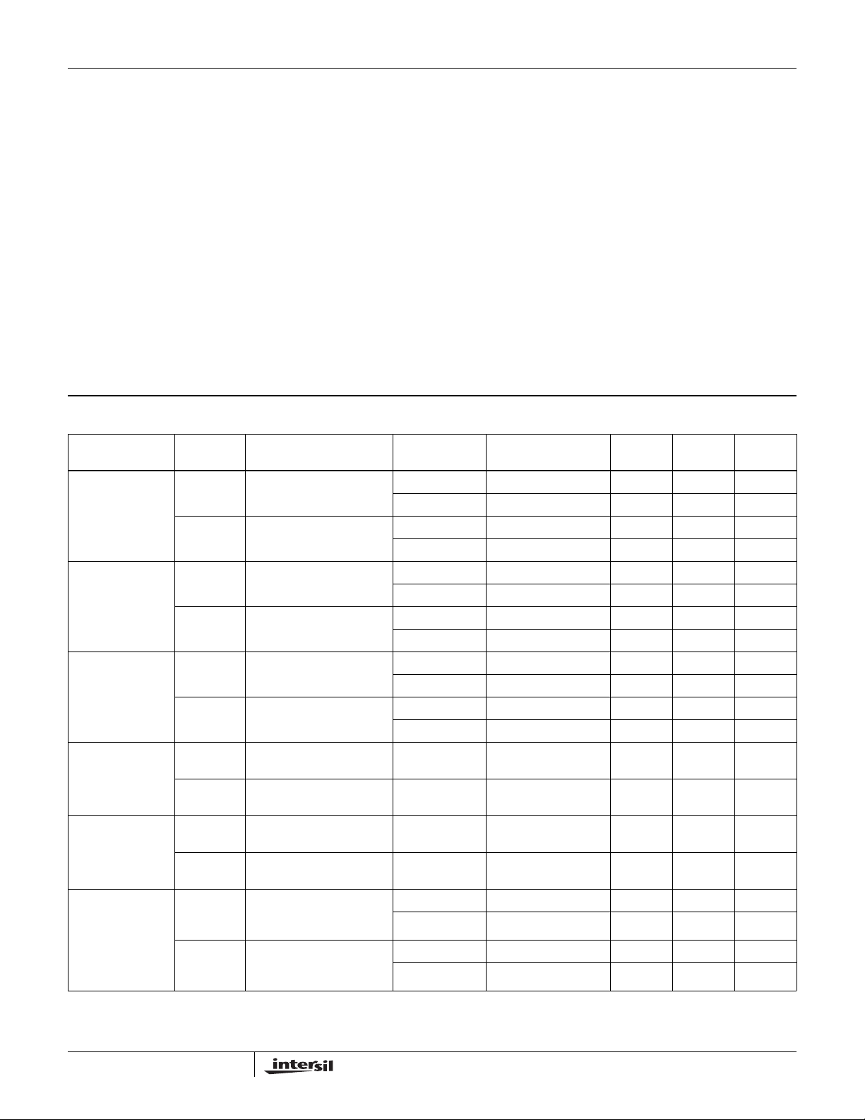
TABLE 1. DC ELECTRICAL PERFORMANCE CHARACTERISTICS
Device Tested at: V
= ±12V and ±15V, R
SUPPLY
SOURCE
PARAMETERS SYMBOL CONDITIONS
V
Input Offset
Voltage
Input Bias Current I
V
IO1
V
IO2
B1
I
B2
Voltage Gain 1 +AV
-AV
Voltage Gain 2 +AV
-AV
Voltage Gain 3 +AV
-AV
Voltage Gain 4 +AV
-AV
1
1
2
2
3
3
4
4
= ±15V 1 +25 -20 20 mV
SUP
V
= ±12V 1 +25 -20 20 mV
SUP
V
= ±15V, RS = 1kΩ 1+25-77µA
SUP
V
= ±12V, RS = 1kΩ 1+25-77µA
SUP
V
= ±12V, RL = 1kΩ,
SUP
V
= 10V
IN
V
= ±12V, RL = 1kΩ,
SUP
= -10V
V
IN
V
= ±12V, RL = 100Ω,
SUP
= 10V
V
IN
V
= ±12V, RL = 100Ω,
SUP
V
= -10V
IN
V
= ±15V, RL = 100Ω,
SUP
= 10V
V
IN
V
= ±15V, RL = 100Ω,
SUP
= -10V
V
IN
V
= ±15V,
SUP
R
= 1kΩ,
L
= +10V
V
IN
V
= ±15V,
SUP
R
= 1kΩ,
L
= -10V
V
IN
= 50Ω, C
LOAD
GROUP A
SUBGROUPS TEMPERATURE (°C) MIN MAX UNITS
Thermal Resistance θ
(°C/W) θJC (°C/W)
JA
Metal Can Package . . . . . . . . . . . . . . . 160 70
Ceramic LCC Package. . . . . . . . . . . . . 80 30
Package Power Dissipation Limit at +75°C for T
Metal Can Package . . . . . . . . . . . . . . . . . . . . . . . . . . . . . .625mW
≤ +175°C
J
Ceramic LCC Package. . . . . . . . . . . . . . . . . . . . . . . . . . . . . 1.25W
Package Power Dissipation Derating Factor Above +75°C
Metal Can Package . . . . . . . . . . . . . . . . . . . . . . . . . . . .6.3mW/°C
Ceramic LCC Package. . . . . . . . . . . . . . . . . . . . . . . . . 12.5mW/°C
≤ 10pF, VIN = 0V, Unless Otherwise Specified.
2, 3 +125, -55 -30 30 mV
2, 3 +125, -55 -30 30 mV
2, 3 +125, -55 -10 10 µA
2, 3 +125, -55 -10 10 µA
1 +25 0.98 - V/V
2, 3 +125, -55 0.98 - V/V
1 +25 0.98 - V/V
2, 3 +125, -55 0.98 - V/V
1 +25 0.96 - V/V
1 +25 0.96 - V/V
1 +25 0.96 - V/V
1 +25 0.96 - V/V
1 +25 0.99 - V/V
2, 3 +125, -55 0.99 - V/V
1 +25 0.99 - V/V
2, 3 +125, -55 0.99 - V/V
2
FN3705.4
January 5, 2006

HA-5002/883
www.BDTIC.com/Intersil
Device Tested at: V
= ±12V and ±15V, R
SUPPLY
SOURCE
PARAMETERS SYMBOL CONDITIONS
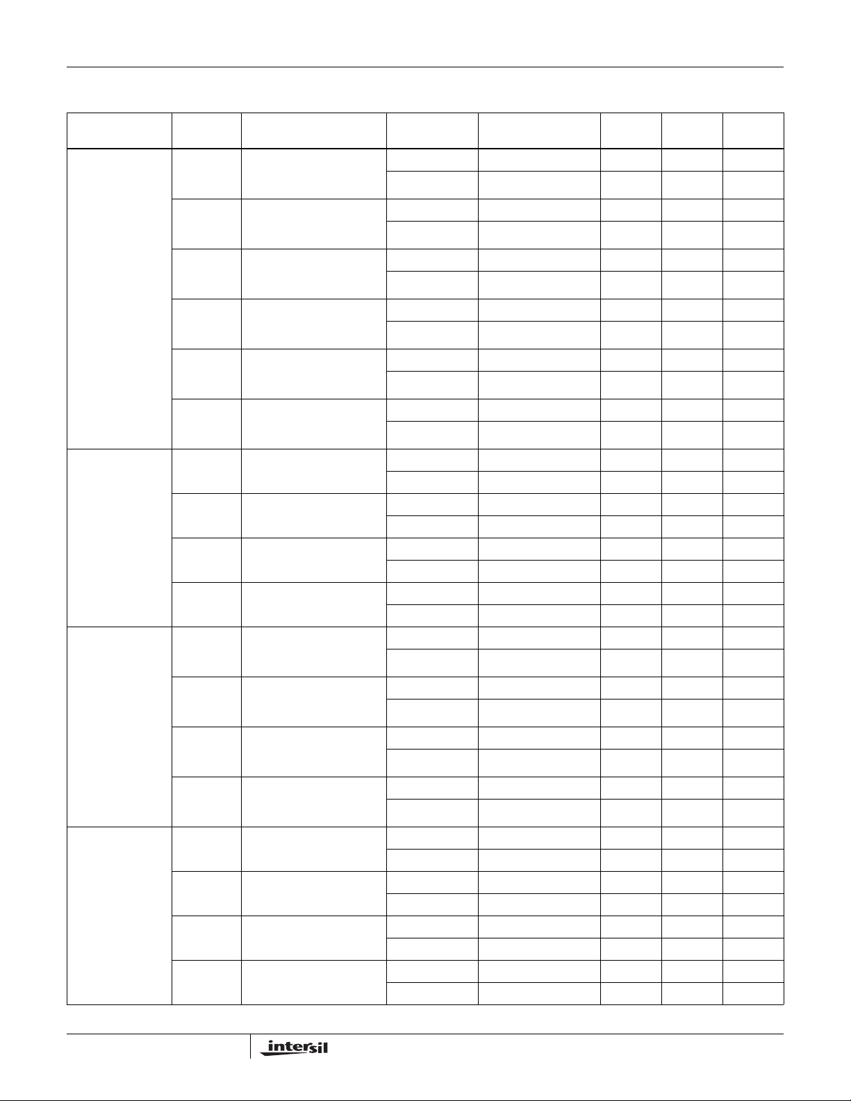
TABLE 1. DC ELECTRICAL PERFORMANCE CHARACTERISTICS (Continued)
Output Voltage
Swing
Output Current +I
Power Supply
Rejection Ratio
+V
OUT1VSUP
-V
OUT1
+V
OUT2VSUP
-V
OUT2
+V
OUT3VSUP
-V
OUT3
OUT1
-I
OUT1
+I
OUT2
-I
OUT2
+PSRR
1
= ±15V,
= 100Ω,
R
L
= +15V
V
IN
V
= ±15V,
SUP
= 100Ω,
R
L
= -15V
V
IN
= ±15V,
= 1kΩ,
R
L
= +15V
V
IN
V
= ±15V,
SUP
= 1kΩ,
R
L
= -15V
V
IN
= ±12V,
= 1kΩ,
R
L
= +12V
V
IN
V
= ±12V,
SUP
= 1kΩ,
R
L
= -12V
V
IN
V
= ±15V,
SUP
V
= +10V
OUT
V
= ±15V,
SUP
= -10V
V
OUT
V
= ±12V,
SUP
= +10V
V
OUT
V
= ±12V,
SUP
V
= -10V
OUT
∆V
= ±5V,
SUP
V+ = +20V, V- = -15V,
V+ = +10V, V- = -15V
∆V
-PSRR
1
SUP
= ±5V,
V+ = +15V, V- = -20V,
V+ = +15V, V- = -10V
∆V
+PSRR
2
SUP
= ±5V,
V+ = +17V, V- = -12V,
V+ = +7V, V- = -12V
∆V
-PSRR
2
SUP
= ±5V,
V+ = +12V, V- = -17V,
V+ = +12V, V- = -7V
V
V
V
V
V
V
V
V
SUP
OUT
SUP
OUT
SUP
OUT
SUP
OUT
= ±15V,
= 0V
= ±15V,
= 0V
= ±12V,
= 0V
= ±12V,
= 0V
Power Supply
Current
+ICC
-ICC
+ICC
-ICC
1
1
2
2
= 50Ω, C
≤ 10pF, VIN = 0V, Unless Otherwise Specified.
LOAD
GROUP A
SUBGROUPS TEMPERATURE (°C) MIN MAX UNITS
1 +25 10 - V
2, 3 +125, -55 10 - V
1 +25 - -10 V
2, 3 +125, -55 - -10 V
1 +25 10 - V
2, 3 +125, -55 10 - V
1 +25 - -10 V
2, 3 +125, -55 - -10 V
1 +25 10 - V
2, 3 +125, -55 10 - V
1 +25 - -10 V
2, 3 +125, -55 - -10 V
1 +25 100 - mA
2, 3 +125, -55 100 - mA
1 +25 - -100 mA
2, 3 +125, -55 - -100 mA
1 +25 100 - mA
2, 3 +125, -55 100 - mA
1 +25 - -100 mA
2, 3 +125, -55 - -100 mA
1 +25 54 - dB
2, 3 +125, -55 54 - dB
1 +25 54 - dB
2, 3 +125, -55 54 - dB
1 +25 54 - dB
2, 3 +125, -55 54 - dB
1 +25 54 - dB
2, 3 +125, -55 54 - dB
1+25-10mA
2, 3 +125, -55 - 10 mA
1+25-10-mA
2, 3 +125, -55 -10 - mA
1+25-10mA
2, 3 +125, -55 - 10 mA
1+25-10-mA
2, 3 +125, -55 -10 - mA
3
FN3705.4
January 5, 2006
 Loading...