HA-5002
November 1998 File Number 2921.4Data Sheet
110MHz, High Slew Rate, High Output
Current Buffer
The HA-5002 is a monolithic, wideband, high slew rate,high
output current, buffer amplifier.
Utilizing the advantages of the Intersil D.I. technologies, the
HA-5002 current buffer offers 1300V/µs slew rate with
110MHz ofbandwidth. The ±200mA output current capability
is enhanced by a 3Ω output impedance.
The monolithic HA-5002 will replace the hybrid LH0002 with
corresponding performance increases. These characteristics
range from the 3000kΩ input impedance to the increased
output voltage swing. Monolithic design technologies ha ve
allowed a more precise bufferto be developed with more than
an order of magnitude smaller gain error.
The HA-5002 will provide many present hybrid users with a
higher degree of reliability and at the same time increase
overall circuit performance.
For the military grade product, refer to the HA-5002/883
datasheet, AnswerFAX document #3705.
Features
• Voltage Gain. . . . . . . . . . . . . . . . . . . . . . . . . . . . . . . 0.995
• High Input Impedance . . . . . . . . . . . . . . . . . . . . . 3000kΩ
• Low Output Impedance . . . . . . . . . . . . . . . . . . . . . . . . 3Ω
• Very High Slew Rate . . . . . . . . . . . . . . . . . . . . . 1300V/µs
• Very Wide Bandwidth . . . . . . . . . . . . . . . . . . . . . . 110MHz
• High Output Current. . . . . . . . . . . . . . . . . . . . . . . ±200mA
• Pulsed Output Current . . . . . . . . . . . . . . . . . . . . . . 400mA
• Monolithic Construction
Applications
• Line Driver
• Data Acquisition
• 110MHz Buffer
• Radar Cable Driver
• High Power Current Booster
• High Power Current Source
• Sample and Holds
• Video Products
Ordering Information
PART NUMBER
(BRAND)
HA2-5002-2 -55 to 125 8 Pin Metal Can T8.C
HA2-5002-5 0 to 75 8 Pin Metal Can T8.C
HA3-5002-5 0 to 75 8 Ld PDIP E8.3
HA4P5002-5 0 to 75 20 Ld PLCC N20.35
HA7-5002-2 -55 to 125 8 Ld CERDIP F8.3A
HA7-5002-5 0 to 75 8 Ld CERDIP F8.3A
HA9P5002-5
(H50025)
HA9P5002-9
(H50029)
TEMP.
RANGE (oC) PACKAGE PKG. NO.
0 to 75 8 Ld SOIC M8.15
-40 to 85 8 Ld SOIC M8.15
Pinouts
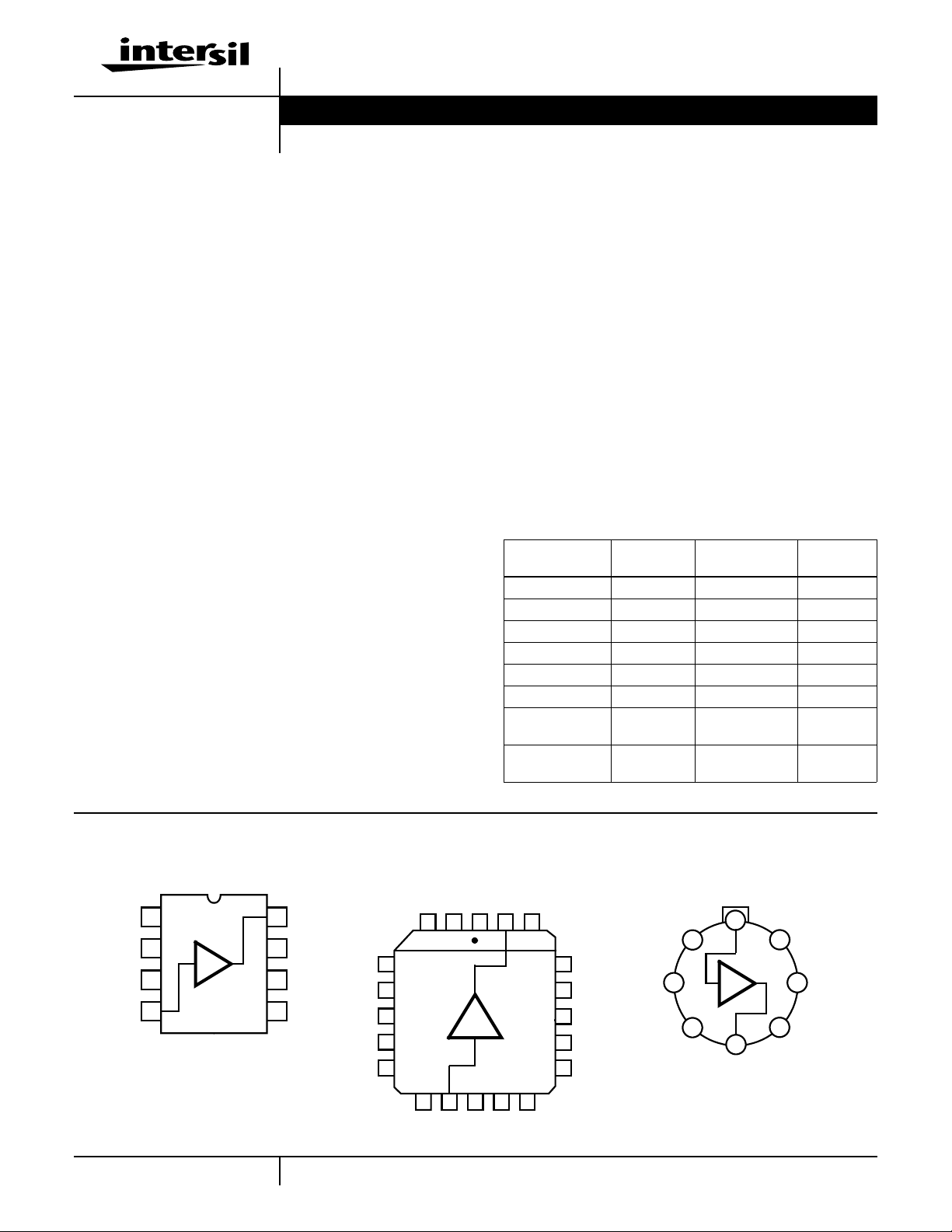
HA-5002 (PDIP, CERDIP, SOIC)
+
V
1
-
V
2
NC
IN
1
2
3
4
TOP VIEW
HA-5002 (PLCC)
TOP VIEW
+
1
V
8
OUT
7
V2+
4
6
NC
5
V
-
1
1
NC
V
-
5
2
6
NC
NC
7
NC
8
CAUTION: These devices are sensitive to electrostatic discharge; follow proper IC Handling Procedures.
NC
9
NC
NC
10 11 12 13
IN
NC
NC
OUT
193 2 201
18
NC
17
V2+
16
NC
15
NC
NC
14
NOTE: Case Voltage = Floating
-
1
NC
V
1-888-INTERSIL or 321-724-7143
HA-5002 (METAL CAN)
TOP VIEW
IN
8
+
V
1
1
2
3
NC
4
OUT
V1-
7
6
5
NC
| Copyright © Intersil Corporation 1999
V2-V2+

HA-5002
Absolute Maximum Ratings Thermal Information
Voltage Between V+ and V- Terminals. . . . . . . . . . . . . . . . . . . . 44V
Input Voltage . . . . . . . . . . . . . . . . . . . . . . . . . . . . . . . . . . V1+ to V1-
Output Current (Continuous) . . . . . . . . . . . . . . . . . . . . . . . . ±200mA
Output Current (50ms On, 1s Off) . . . . . . . . . . . . . . . . . . . . ±400mA
Operating Conditions
Temperature Range
HA-5002-2 . . . . . . . . . . . . . . . . . . . . . . . . . . . . . . -55oC to 125oC
HA-5002-5 . . . . . . . . . . . . . . . . . . . . . . . . . . . . . . . . 0oC to 75oC
HA-5002-9 . . . . . . . . . . . . . . . . . . . . . . . . . . . . . . . -40oC to 85oC
CAUTION: Stresses above those listed in “Absolute Maximum Ratings” may cause permanent damage to the device. This is a stress only rating and operation of the
device at these or any other conditions above those indicated in the operational sections of this specification is not implied.
NOTES:
1. Maximum power dissipation, including load conditions, must be designed to maintain the maximum junction temperature below 175oC for the
ceramic and can packages, and below 150oC for the plastic packages.
2. θJA is measured with the component mounted on an evaluation PC board in free air.
Thermal Resistance (Typical, Note 2) θJA (oC/W)θJC (oC/W)
CERDIP Package. . . . . . . . . . . . . . . . . 115 28
PDIP Package . . . . . . . . . . . . . . . . . . . 92 N/A
Metal Can Package . . . . . . . . . . . . . . . 155 67
PLCC Package. . . . . . . . . . . . . . . . . . . 74 N/A
SOIC Package . . . . . . . . . . . . . . . . . . . 157 N/A
Max Junction Temperature (Hermetic Packages , Note 1). . . . . . 175oC
Max Junction Temperature (Plastic Pac kages , Note 1) . . . . . . . . 150oC
Max Storage Temperature Range . . . . . . . . . . . . . . -65oC to 150oC
Max Lead Temperature (Soldering 10s) . . . . . . . . . . . . . . . . 300oC
(PLCC and SOIC - Lead Tips Only)
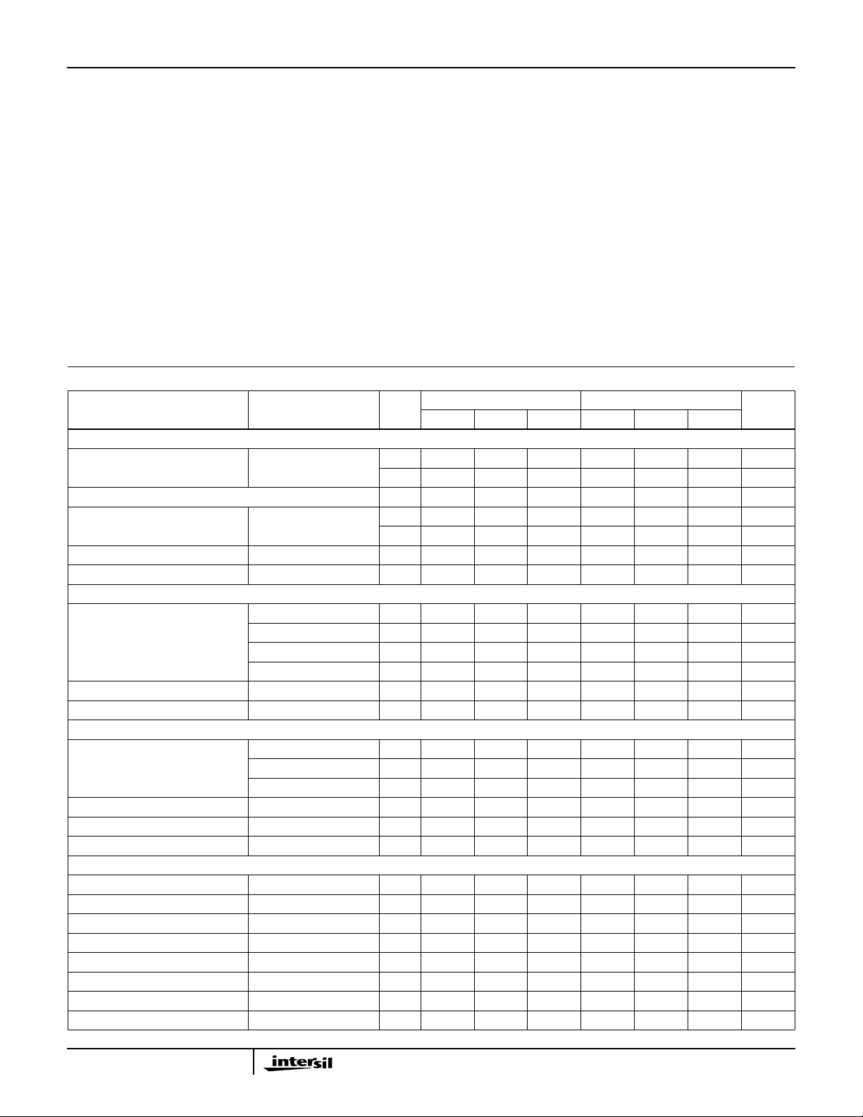
Electrical Specifications V
PARAMETER
= ±12V to ±15V, RS = 50Ω, RL = 1kΩ, CL = 10pF, Unless Otherwise Specified
SUPPLY
TEST
CONDITIONS
TEMP
(oC)
HA-5002-2 HA-5002-5, -9
UNITSMIN TYP MAX MIN TYP MAX
INPUT CHARACTERISTICS
Offset Voltage 25 - 5 20 - 5 20 mV
Full - 10 30 - 10 30 mV
Average Offset Voltage Drift Full - 30 - - 30 - µV/
Bias Current 25 - 2 7 - 2 7 µA
Full - 3.4 10 - 2.4 10 µA
Input Resistance Full 1.5 3 - 1.5 3 - MΩ
Input Noise Voltage 10Hz-1MHz 25 - 18 - - 18 - µV
TRANSFER CHARACTERISTICS
Voltage Gain
= ±10V)
(V
OUT
-3dB Bandwidth V
RL = 50Ω 25 - 0.900 - - 0.900 - V/V
= 100Ω 25 - 0.971 - - 0.971 - V/V
R
L
R
= 1kΩ 25 - 0.995 - - 0.995 - V/V
L
= 1kΩ Full 0.980 - - 0.980 - - V/V
R
L
IN
= 1V
P-P
25 - 110 - - 110 - MHz
AC Current Gain 25 - 40 - - 40 - A/mA
OUTPUT CHARACTERISTICS
Output Voltage Swing R
Output Current V
= 100Ω 25 ±10 ±10.7 - ±10 ±11.2 - V
L
= 1kΩ, VS = ±15V Full ±10 ±13.5 - ±10 ±13.9 - V
R
L
= 1kΩ, VS = ±12V Full ±10 ±10.5 - ±10 ±10.5 - V
R
L
= ±10V, RL = 40Ω 25 - 220 - - 220 - mA
IN
Output Resistance Full - 3 10 - 3 10 Ω
Harmonic Distortion V
IN
= 1V
, f = 10kHz 25 - <0.005 - - <0.005 - %
RMS
TRANSIENT RESPONSE
Full Power Bandwidth (Note 3) 25 - 20.7 - - 20.7 - MHz
Rise Time 25 - 3.6 - - 3.6 - ns
Propagation Delay 25 - 2 - - 2 - ns
Overshoot 25 - 30 - - 30 - %
Slew Rate 25 1.0 1.3 - 1.0 1.3 - V/ns
Settling Time To 0.1% 25 - 50 - - 50 - ns
Differential Gain R
Differential Phase R
= 500Ω 25 - 0.06 - - 0.06 - %
L
= 500Ω 25 - 0.22 - - 0.22 - Degrees
L
ο
P-P
C
2

HA-5002
Electrical Specifications V
PARAMETER
= ±12V to ±15V, RS = 50Ω, RL = 1kΩ, CL = 10pF, Unless Otherwise Specified (Continued)
SUPPLY
TEST
CONDITIONS
TEMP
(oC)
HA-5002-2 HA-5002-5, -9
UNITSMIN TYP MAX MIN TYP MAX
POWER REQUIREMENTS
Supply Current 25 - 8.3 - - 8.3 - mA
Full - - 10 - - 10 mA
Power Supply Rejection Ratio A
= 10V Full 54 64 - 54 64 - dB
V
NOTE:
3. .
PBW
Slew Rate
---------------------------
2πV
P
EAK
;VP= 10V=
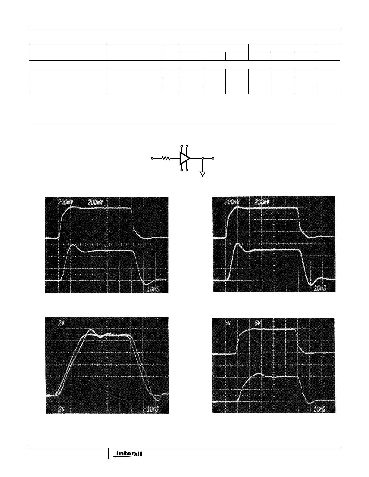
Test Circuit and Waveforms
+15V
-15V
+
V
2
OUTIN
V
-V1-
2
R
L
V1+
R
S
FIGURE 1. LARGE AND SMALL SIGNAL RESPONSE
V
V
V
OUT
V
OUT
V
V
OUT
IN
RS = 50Ω, RL = 1kΩ
IN
RS = 50Ω, RL = 100Ω
SMALL SIGNAL WAVEFORMS SMALL SIGNAL WAVEFORMS
IN
V
V
OUT
IN
RS = 50Ω, RL = 100Ω
RS = 50Ω, RL = 1kΩ
LARGE SIGNAL WAVEFORMS LARGE SIGNAL WAVEFORMS
3

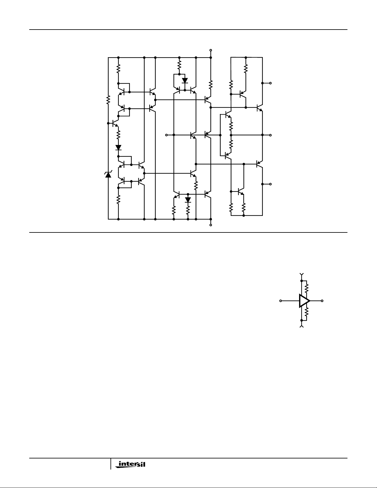
Schematic Diagram
HA-5002
V
+
1
R
R
9
Q
25
R
10
Q
9
Q
10
R
5
Q
21
Q
11
Q
15
Q
23
R
7
Q
22
Q
24
8
Q
19
R
Q
20
Q
26
Q
27
IN
Q
16
R
12
Q
Q7Q
Q
8
R
Q
17
R
3
4
18
Q
3
4
6
Q
14
R
2
R
N1
R
1
Q
12
Q
6
R
11
R
N2
Q
5
Q
13
R
N3
V2+
Q
1
OUT
Q
2
V2-
Application Information
Layout Considerations
The wide bandwidth of the HA-5002 necessitates that high
frequency circuit layout procedures be followed. Failure to
follow these guidelines can result in marginal performance.
Probably the most crucial of the RF/video layout rules is the
use of a ground plane. A ground plane provides isolation and
minimizes distributed circuit capacitance and inductance
which will degrade high frequency performance.
Other considerations are proper power supply bypassing
and keeping the input and output connections as short as
possible which minimizes distributed capacitance and
reduces board space.
Power Supply Decoupling
For optimal device performance, it is recommended that the
positive and negative power supplies be bypassed with
capacitors to ground. Ceramic capacitors ranging in value
from 0.01 to 0.1µF will minimize high frequency variations in
supply voltage, while low frequency bypassing requires
larger valued capacitors since the impedance of the
capacitor is dependent on frequency.
It is also recommended that the bypass capacitors be
connected close to the HA-5002 (preferably directly to the
supply pins).
Operation at Reduced Supply Levels
The HA-5002 can operate at supply voltage levels as low as
±5V and lower. Output swing is directly affected as well as
slight reductions in slew rate and bandwidth.
V1-
Short Circuit Protection
The output current can be limited by using the following circuit:
I
R
LIM
V+
------------------------- -
I
OUTMAX
V-
------------------------- -==
I
OUTMAX
V+
V
+
1
IN
V1-
V-
= 200mA
OUTMAX
(CONTINUOUS)
R
LIM
V2+
OUT
V
-
2
R
LIM
Capacitive Loading
The HA-5002 will drive large capacitive loads without oscillation
but peak current limits should not be exceeded. F ollo wing the
formula I = Cdv/dt implies that the slew rate or the capacitive
load must be controlled to keep peak current below the
maximum or use the current limiting approach as shown. The
HA-5002 can become unstable with small capacitive loads
(50pF) if certain precautions are not taken. Stability is
enhanced by any one of the follo wing: a source resistance in
series with the input of 50Ω to 1kΩ; increasing capacitive load
to 150pF or greater; decreasing C
an output resistor of 10Ω to 50Ω; or adding feedback
capacitance of 50pF or greater. Adding source resistance
generally yields the best results.
to 20pF or less; adding
LOAD
4
 Loading...