Intersil Corporation HA-4741-883 Datasheet

HA-4741/883
July 1994
Features
• This Circuit is Processed in Accordance to MIL-STD883 and is Fully Conformant Under the Provisions of
Paragraph 1.2.1.
• Slew Rate . . . . . . . . . . . . . . . . . . . . . . . . . . 0.9V/µs (Min)
• Bandwidth. . . . . . . . . . . . . . . . . . . . . . . . . . 2.5MHz (Min)
• Input Offset Voltage. . . . . . . . . . . . . . . . . . . . 3mV (Max)
• Input Bias Current . . . . . . . . . . . . . . . . . . . 200nA (Max)
• Input Voltage Noise . . . . . . . . . . . . . . . . . 9nV/√
Hz (Typ)
• No Crossover Distortion
• Standard Quad Pinout
Applications
• Universal Active Filters
• D3 Communications Filters
• Audio Amplifiers
• Battery-Powered Equipment
Quad Operational Amplifier
Description
The Harris HA-4741/883, which contains four amplifiers on a
monolithic chip, provides a new measure of performance for
general purpose operational amplifiers. Each amplifier in the
HA-4741/883 has operating specifications that equal or
exceed those of the 741-type amplifier in all categories of
performance.
The HA-4741/883 is well suited to applications requiring accurate signal processing by virtue of its low values of input offset
voltage (3mV max ), input bias current (200nA max) and input
voltage noise (9nV/√
coupled with high open loop gain, allow the HA-4741/883 to be
used in designs requiring amplifiers of wideband signals, such
as audio amplifiers. Audio application is further enhanced by
the HA-4741/883’s negligible output crossover distortion. These
excellent dynamic characteristics also make the HA-4741/883
ideal for a wide range of active filter designs. Performance
integrity of multi-channel designs is assured by a high level of
amplifier-to-amplifier isolation (66dB at 10kHz).
A wide range of supply voltages (±2V to ±20V) can be used
to power the HA-4741/883, making it compatible with almost
any system including battery-powered equipment.
Hz typ at 1kHz). The 2.5MHz bandwidth,
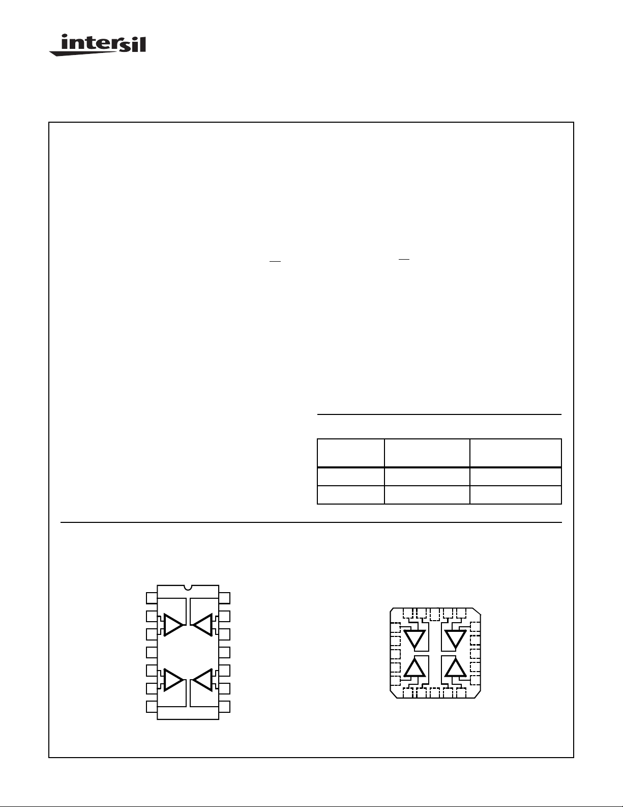
Pinouts
OUT1
-IN1
+IN1
V+
+IN2
-IN2
OUT2
HA-4741/883
(CERDIP)
TOP VIEW
1
2
-
1
+
3
4
5
+
2
-
6
7
Ordering Information
PART
NUMBER
HA1-4741/883 -55oC to +125oC 14 Lead CerDIP
HA4-4741/883 -55oC to +125oC 20 Lead Ceramic LCC
OUT4
14
-IN4
13
-
4
+
12
+IN4
V-
11
10
+IN3
+
3
-
-IN3
9
8
OUT3
TEMPERATURE
+IN1
4
NC
5
V+
6
NC
7
+IN2
8
RANGE PACKAGE
HA-4741/883
(CLCC)
TOP VIEW
OUT1NCOUT4
-IN1
3212019
-
+
1
2
-
+
9101112
-IN2
OUT2NCOUT3
-IN4
+IN4
18
-
+
4
17
NC
V-
16
3
-
NC
15
+
14
+IN3
13
-IN3
CAUTION: These devices are sensitive to electrostatic discharge; follow proper IC Handling Procedures.
http://www.intersil.com or 407-727-9207
| Copyright © Intersil Corporation 1999
3-112
Spec Number
File Number 3704
511007-883

Specifications HA-4741/883
Absolute Maximum Ratings Thermal Information
Voltage Between V+ and V- Terminals . . . . . . . . . . . . . . . . . . . . 40V
Differential Input Voltage . . . . . . . . . . . . . . . . . . . . . . . . . . . . . . 15V
Voltage at Either Input Terminal . . . . . . . . . . . . . . . . . . . . . . V+ to V-
Output Current . . . . . . . . Indefinite (One Amplifier Shorted to GND)
Junction Temperature (TJ) . . . . . . . . . . . . . . . . . . . . . . . . . . +175oC
Storage Temperature Range . . . . . . . . . . . . . . . . . -65oC to +150oC
ESD Rating. . . . . . . . . . . . . . . . . . . . . . . . . . . . . . . . . . . . . . <2000V
Lead Temperature (Soldering 10s). . . . . . . . . . . . . . . . . . . . +300oC
CAUTION: Stresses above those listed in “Absolute Maximum Ratings” may cause permanent damage to the device. This is a stress only rating and operation
of the device at these or any other conditions above those indicated in the operational sections of this specification is not implied.
Operating Conditions
Operating Temperature Range. . . . . . . . . . . . . . . . -55oC to +125oC
Operating Supply Voltage. . . . . . . . . . . . . . . . . . . . . . . . . . ±5V to ±15V
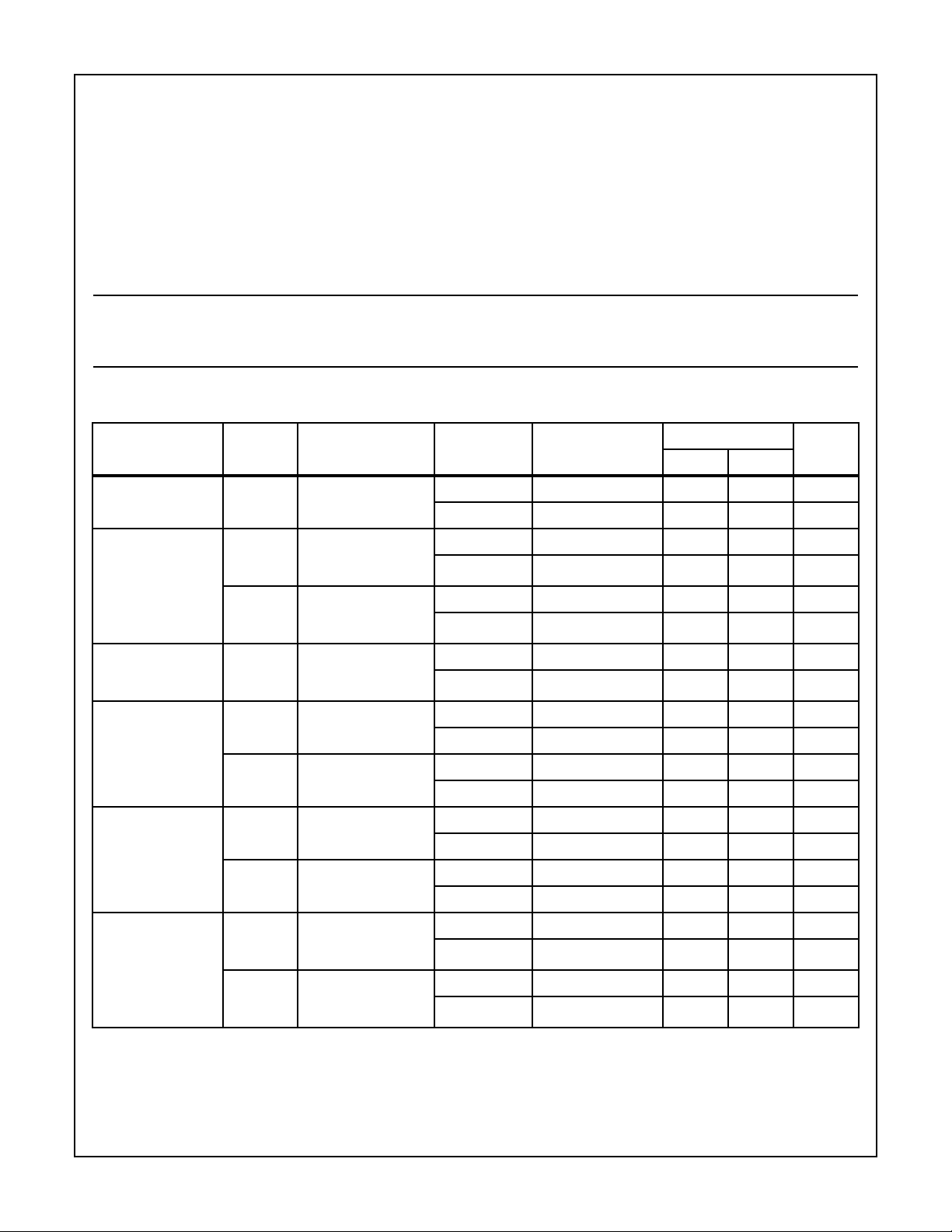
TABLE 1. DC ELECTRICAL PERFORMANCE CHARACTERISTICS
Device Tested at: V
PARAMETERS SYMBOL CONDITIONS
Input Offset Voltage V
Input Bias Current +I
Input Offset Current I
Common Mode
Range
Large Signal Voltage
Gain
Common Mode
Rejection Ratio
SUPPLY
= ±15V, R
IO
B
SOURCE
= 100Ω, R
LOAD
= 500kΩ, V
VCM = 0V 1 +25oC-33mV
VCM = 0V,
+RS = 10kΩ,
-RS = 100Ω
-I
VCM = 0V,
B
+RS = 100Ω,
-RS = 10kΩ
IO
VCM = 0V,
+RS = 10kΩ,
-RS = 10kΩ
+CMR V+ = 3V, V- = -27V 1 +25oC12-V
-CMR V+ = 27V, V- = -3V 1 +25oC - -12 V
+A
VOL
V
= 0V and +10V,
OUT
RL = 2kΩ
-A
VOL
V
= 0V and -10V,
OUT
RL = 2kΩ
+CMRR ∆VCM = -10V,
V+ = +5V, V- = -25V,
V
= -10V
OUT
-CMRR ∆VCM = +10V,
V+ = +25V, V- = -5V,
V
= +10V
OUT
Thermal Resistance θ
JA
CerDIP Package . . . . . . . . . . . . . . . . . . . 75oC/W 20oC/W
Ceramic LCC Package . . . . . . . . . . . . . . 65oC/W 15oC/W
Package Power Dissipation Limit at +75oC for TJ≤ +175oC
CerDIP Package . . . . . . . . . . . . . . . . . . . . . . . . . . . . . . . . .1.33W
Ceramic LCC Package . . . . . . . . . . . . . . . . . . . . . . . . . . . . 1.54W
Package Power Dissipation Derating Factor Above +75oC
CerDIP Package . . . . . . . . . . . . . . . . . . . . . . . . . . . . .13.3mW/oC
Ceramic LCC Package . . . . . . . . . . . . . . . . . . . . . . . .15.4mW/oC
V
≤ 1/2 (V+ - V-)
INCM
RL≥ 2kΩ
= 0V, Unless Otherwise Specified.
OUT
GROUP A
SUBGROUPS TEMPERATURE
LIMITS
UNITSMIN MAX
2, 3 +125oC, -55oC-5 5mV
1 +25oC -200 200 nA
2, 3 +125oC, -55oC -325 325 nA
1 +25oC -200 200 nA
2, 3 +125oC, -55oC -325 325 nA
1 +25oC -30 30 nA
2, 3 +125oC, -55oC -75 75 nA
2, 3 +125oC, -55oC12 - V
2, 3 +125oC, -55oC - -12 V
4 +25oC 50 - kV/V
5, 6 +125oC, -55oC 25 - kV/V
4 +25oC 50 - kV/V
5, 6 +125oC, -55oC 25 - kV/V
1 +25oC80-dB
2, 3 +125oC, -55oC74 - dB
1 +25oC80-dB
2, 3 +125oC, -55oC74 - dB
θ
JC
3-113
Spec Number 511007-883
 Loading...