HA-4741
Data Sheet September 1998 File Number 2922.3
Quad, 3.5MHz, Operational Amplifier
HA-4741, which contains four amplifiers on a monolithic
chip, provides a new measure of performance for general
purpose operational amplifiers. Each amplifier in the
HA-4741 has operating specifications that equal or exceed
those of the 741-type amplifier in all categories of
performance.
HA-4741 is well suited to applications requiring accurate
signal processing by virtue of its low values of input offset
voltage (0.5mV), input bias current (60nA) and input voltage
noise (9nV/√
Hz at 1kHz). 3.5MHz bandwidth, coupled with
high open-loop gain, allow the HA-4741 to be used in
designs requiring amplification ofwideband signals, such as
audio amplifiers. Audio application is further enhanced by
the HA-4741’s negligible output crossover distortion.
These excellent dynamic characteristics also make the
HA-4741 ideal for a wide range of active filter designs.
Performance integrity of multi-channel designs is assured by
a high level of amplifier-to-amplifier isolation (69dB at
10kHz).
A wide range of supply voltages (±2V to ±20V) can be used
to power the HA-4741, making it compatible with almost any
system including battery-powered equipment.
HA-4741/883 product and data sheets available upon
request.
Ordering Information
PART
NUMBER
HA1-4741-2 -55 to 125 14 Ld CERDIP F14.3
HA1-4741-5 0 to 75 14 Ld CERDIP F14.3
HA3-4741-5 0 to 75 14 Ld PDIP E14.3
HA9P4741-9 -40 to 85 16 Ld SOIC M16.3
TEMP.
RANGE (oC) PACKAGE PKG. NO.
Features
• Slew Rate. . . . . . . . . . . . . . . . . . . . . . . . . . . . . . . 1.6V/µs
• Bandwidth. . . . . . . . . . . . . . . . . . . . . . . . . . . . . . . 3.5MHz
• Input Voltage Noise . . . . . . . . . . . . . . . . . . . . . . 9nV/√
Hz
• Input Offset Voltage . . . . . . . . . . . . . . . . . . . . . . . . 0.5mV
• Input Bias Current . . . . . . . . . . . . . . . . . . . . . . . . . . 60nA
• Supply Range. . . . . . . . . . . . . . . . . . . . . . . . ±2V to ±20V
• No Crossover Distortion
• Standard Quad Pinout
Applications
• Universal Active Filters
• D3 Communications Filters
• Audio Amplifiers
• Battery-Powered Equipment
Pinouts
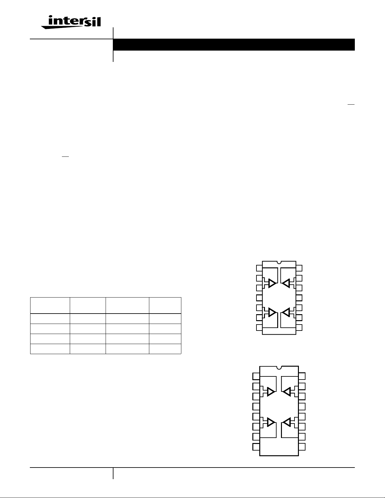
HA-4741
(PDIP, CERDIP)
TOP VIEW
OUT1
-IN1
+IN1
V+
+IN2
-IN2
OUT2
1
2
-
+
3
4
5
+
-
6
7
HA-4741
TOP VIEW
1 4
2 3
(SOIC)
14
OUT4
13
-IN4
-
+
12
+IN4
11
V-
10
+IN3
+
-
9
-IN3
8
OUT3
OUT1
1
2
3
4
5
6
7
8
14
-
+
+
-
| Copyright © Intersil Corporation 1999
-IN1
+IN1
V+
+IN2
-IN2
OUT2
NC
1
CAUTION: These devices are sensitive to electrostatic discharge; follow proper IC Handling Procedures.
1-888-INTERSIL or 321-724-7143
16
OUT4
15
-IN4
-
+
14
+IN4
13
V-
32
12
+IN3
+
-
11
-IN3
10
OUT3
9
NC

HA-4741
Absolute Maximum Ratings Thermal Information
TA = 25oC Unless Otherwise Stated
Supply Voltage Between V+ and V- Terminals. . . . . . . . . . . . . . 40V
Differential Input Voltage . . . . . . . . . . . . . . . . . . . . . . . . . . . . . . 30V
Input Voltage . . . . . . . . . . . . . . . . . . . . . . . . . . . . . . . . . . . V
Output Short Circuit Duration (Note 3). . . . . . . . . . . . . . . . Indefinite
SUPPLY
Operating Conditions
Temperature Range:
HA-4741-2 . . . . . . . . . . . . . . . . . . . . . . . . . . . . . . -55oC to 125oC
HA-4741-5 . . . . . . . . . . . . . . . . . . . . . . . . . . . . . . . . 0oC to 75oC
HA-4741-9 . . . . . . . . . . . . . . . . . . . . . . . . . . . . . . . -40oC to 85oC
CAUTION: Stresses above those listed in “Absolute Maximum Ratings” may cause permanent damage to the device. This is a stress only rating and operation of the
device at these or any other conditions above those indicated in the operational sections of this specification is not implied.
NOTES:
1. Maximum power dissipation, including output load, must be designed to maintain junction temperature below 175oC for the ceramic package,
and below 150oC for the plastic packages.
2. θJA is measured with the component mounted on an evaluation PC board in free air.
3. One amplifier may be shorted to ground indefinitely.
Thermal Resistance (Typical, Note 2) θJA (oC/W) θJC (oC/W)
CERDIP Package. . . . . . . . . . . . . . . . . 90 35
PDIP Package . . . . . . . . . . . . . . . . . . . 107 N/A
SOIC Package . . . . . . . . . . . . . . . . . . . 96 N/A
Maximum Junction Temperature (Ceramic P ac kage, Note 1). . . . .175oC
Maximum Junction Temperature (Plastic P ackages , Note 1) . . . . .150oC
Maximum Storage Temperature Range. . . . . . . . . . -65oC to 150oC
Maximum Lead Temperature (Soldering 10s) . . . . . . . . . . . . 300oC
(SOIC - Lead Tips Only)
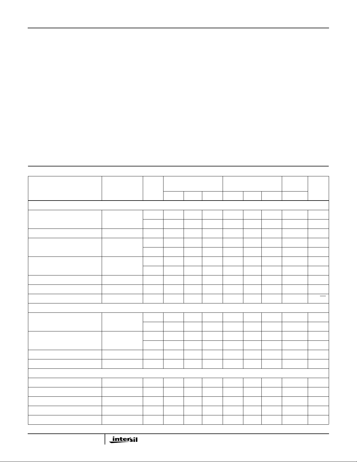
Electrical Specifications V
PARAMETER
INPUT CHARACTERISTICS
Offset Voltage 25 - 0.5 3 - 1 5 5 mV
Average Offset Voltage Drift Full - 5 - - 5 - - µV/oC
Bias Current 25 - 60 200 - 60 300 300 nA
Offset Current 25 - 15 30 - 30 50 50 nA
Common Mode Range Full ±12 - - ±12 - - - V
Differential Input Resistance 25 - 0.5 - - 0.5 - - MΩ
Input Voltage Noise f = 1kHz 25 - 9 - - 9 - - nV/√Hz
TRANSFER CHARACTERISTICS
Large Signal Voltage Gain V
Common Mode Rejection Ratio 25 80 95 - 80 95 - - dB
Channel Separation (Note 5) 25 66 69 - 66 69 - - dB
Small Signal Bandwidth 25 2.5 3.5 - 2.5 3.5 - - MHz
OUTPUT CHARACTERISTICS
Output Voltage Swing RL = 10kΩ Full ±12 ±13.7 - ±12 ±13.7 - - V
Output Voltage Swing RL = 2kΩ Full ±10 ±12.5 - ±10 ±12.5 - - V
Full Power Bandwidth (Notes 6, 7) 25 - 25 - - 25 - - kHz
Output Current V
Output Resistance 25 - 300 - - 300 - - Ω
= ±15V, Unless Otherwise Specified
SUPPLY
(NOTE 4)
TEST
CONDITIONS
= ±10V ,
OUT
RL=2kΩ
= ±10V Full ±5 ±15 - ±5 ±15 - - mA
OUT
TEMP.
(oC)
Full - 4 5 - 4 6.5 8.5 mV
Full - - 325 - - 400 400 nA
Full - - 75 - - 100 100 nA
25 50 100 - 25 50 - - kV/V
Full 25 - - 15 - - - kV/V
Full 74 - - 74 - - - dB
HA-4741-2 HA-4741-5
HA-4741-9
UNITSMIN TYP MAX MIN TYP MAX MAX
2
 Loading...