Intersil Corporation HA456 Datasheet

HA456
Data Sheet August 1999
120MHz, Low Power, 8 x 8 Video
Crosspoint Switch
The HA456 is the first 8 x 8 video crosspoint switch suitable
for high performance video systems. Its high level of
integration significantly reduces component count, board
space, and cost. The crosspoint switch contains a digitally
controlled matrix of 64 fully buffered switches that connect
eight video input signals to any, or all, matrix outputs. Each
matrix output connects to aninternal, high-speed(200V/µs),
unity gain buffer capable of driving 400Ω and 5pF to ±2V.
For applications requiring gain or increased drive capability,
the HA456 outputs can be connected directly to two
HFA1412 quad, gain of two videobuffers,whicharecapable
of driving 75Ω loads.
This crosspoint’s true high impedance three-state output
capability, makes it feasible to parallel multiple HA456s and
form larger switch matrices.
File Number 4153.2
Features
• Fully Buffered Inputs and Outputs (AV= +1)
• Routes Any Input Channel to Any Output Channel
• Switches Standard and High Resolution Video Signals
• Serial or Parallel Digital Interface
• Expandable for Larger Switch Matrices
• Wide Bandwidth . . . . . . . . . . . . . . . . . . . . . . . . . . 120MHz
• High Slew Rate. . . . . . . . . . . . . . . . . . . . . . . . . . . 200V/µs
• Differential Gain and Phase . . . . . . .0.05%, 0.05 Degrees
• Low Crosstalk at 10MHz . . . . . . . . . . . . . . . . . . . . . -55dB
Applications
• Professional Video Switching and Routing
• Security and Video Editing Systems
Ordering Information
TEMP.
PART NUMBER
HA456CN 0 to 70 44 Ld MQFP Q44.10x10
HA456CM 0 to 70 44 Ld PLCC N44.65
RANGE (oC) PACKAGE PKG. NO.
Pinouts
DGND
DGND
EDGE/
LEVEL
A0
IN1
NC
IN2
NC
IN3
IN4
IN5
HA456 (MQFP)
TOP VIEW
IN0A1A2
44 43 42 41 40
1
2
3
4
5
6
7
8
9
10
11
12 13 14 15 16 17
V+
IN6
D0/SER IN
IN7
PAR
SER/
D1/SER OUT
NCV+OUT0D2OUT1
39 38 37 36 35 34
V-
NC
WR
CE
LATCH
CE
2221201918
D3
33
32
31
30
29
28
27
26
25
24
23
OUT7
OUT2
V-
OUT3
AGND
OUT4
NC
AGND
OUT5
AGND
OUT6
V+
EDGE/
A0
IN1
NC
IN2
DGND
NC
IN3
DGND
IN4
LEVEL
IN5
HA456 (PLCC)
IN0A1A2
7
8
9
10
11
12
13
14
15
16
17
V+
IN6
TOP VIEW
D0/SER IN
D1/SER OUT
V-
IN7
PAR
SER/
NCV+OUT0D2OUT1
44 43 42 41 40
123456
262524232221201918
CE
WR
CE
LATCH
NC
D3
2827
39
38
37
36
35
34
33
32
31
30
29
OUT7
OUT2
VOUT3
AGND
OUT4
NC
AGND
OUT5
AGND
OUT6
V+
1
CAUTION: These devices are sensitive to electrostatic discharge; follow proper IC Handling Procedures.
1-888-INTERSIL or 321-724-7143
| Copyright © Intersil Corporation 1999

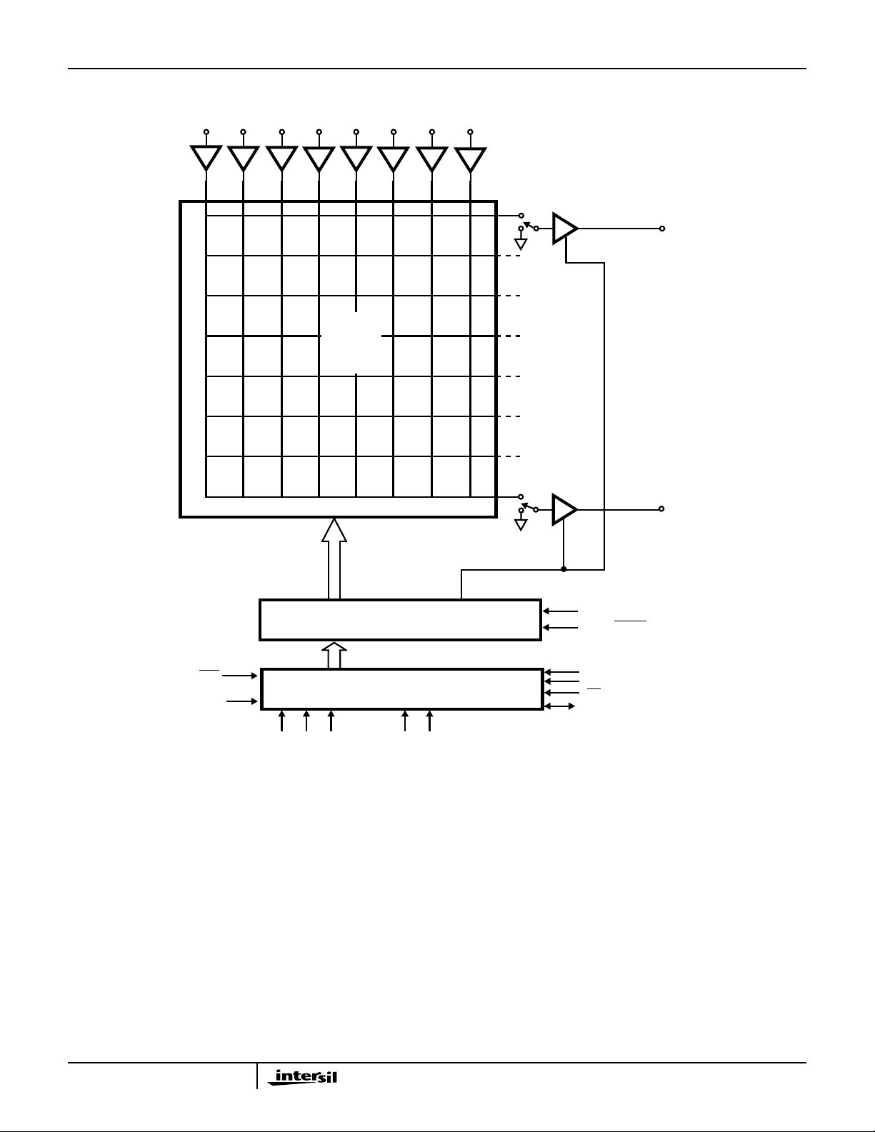
HA456 Functional Block Diagram
IN0 IN2 IN3 IN4 IN5 IN6 IN7IN1
HA456
8 x 8
SWITCH
MATRIX
HA456
OUTPUT
BUFFERS
(AV = 1)
EN0
OUT0
SER/PAR
D0/SER IN
SLAVE REGISTER
MASTER REGISTER
A0 A1 A2 D2 D3
EN0:7
EN7
LATCH
EDGE/
LEVEL
WR
CE
CE
D1/SER OUT
OUT7
2

HA456
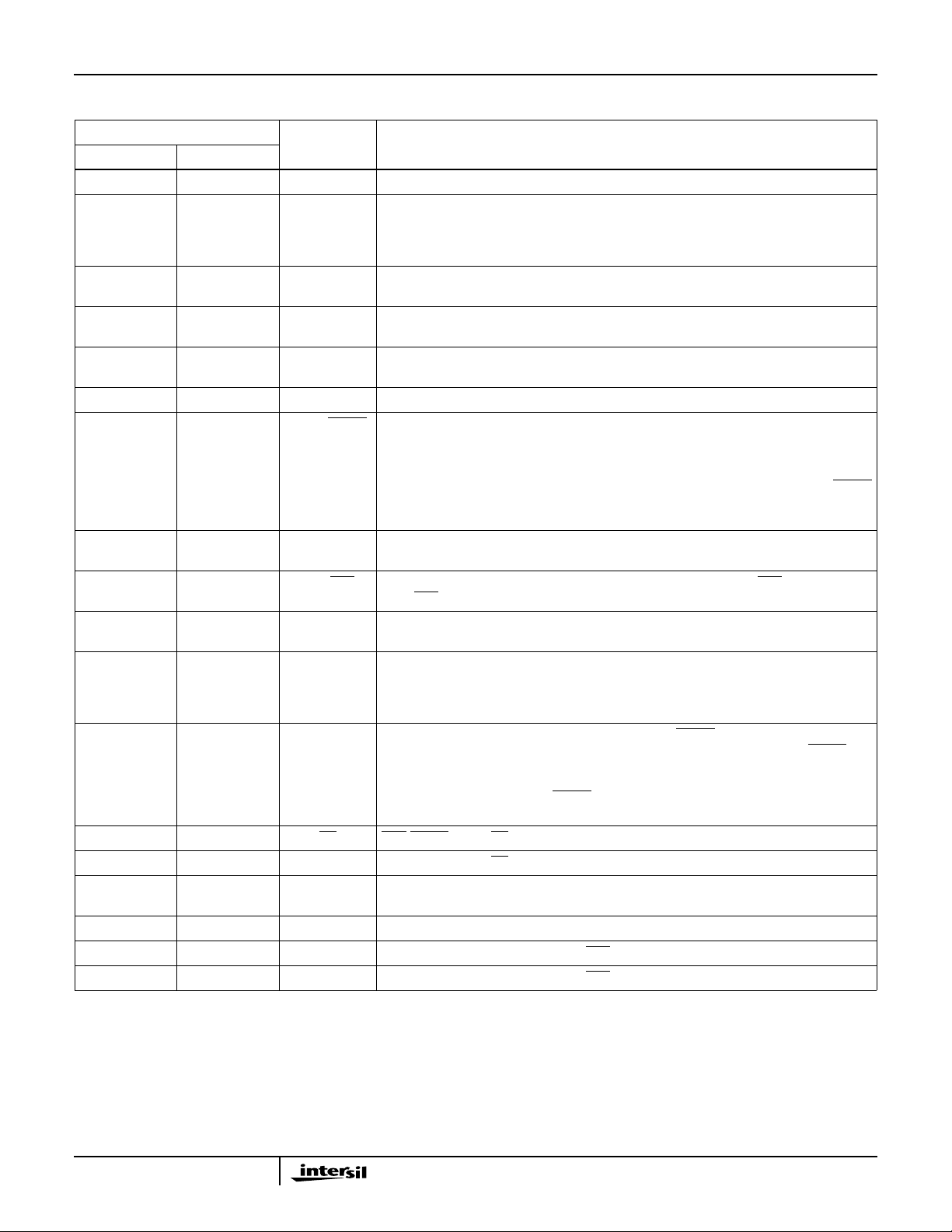
Pin Description
PIN
NAME FUNCTIONMQFP PLCC
3, 6, 17, 28, 39 1, 9, 12, 23, 34 NC No connect. Not internally connected.
40 2 D1/ SER OUT Parallel Data Bit input D1 for Parallel Programming Mode. Serial Data Output (MSB of shift
register) for cascading multiple HA456s in serial programming mode. Simply connect
Serial Data Out of one HA456 to Serial Data In of another HA456 to daisy chain multiple
devices.
41 3 D0/SER IN Parallel Data Bit Input D0 for Parallel Programming Mode. Serial Data Input (input to shift
register) for serial programming mode.
42, 43, 1 4, 5, 7 A2, A1, A0 OutputChannelAddress Bits. These inputs select the output being programmed in parallel
programming mode.
44, 2, 4, 7, 9, 11,
13, 15
5, 8 11, 14 DGND Digital Ground. Connect both DGND pins to AGND.
10 16 EDGE/LEVEL A user strapped input that defines whether synchronous channel switching is edge or level
12, 23, 38 18, 29, 44 V+ Positive Supply Voltage. Connect all V+ pins together and decouple each pin to AGND
14 20 SER/PAR A user strapped input that defines whether the serial (SER/PAR=1) or parallel
16, 32 22, 38 V- Negative Supply Voltage. Connect both V- pins together and decouple each pin to AGND
18 24 WR WRITE Input. In serial mode, data shifts into the shift register (Master Register) LSB from
19 25 LATCH Synchronous Channel Switch Control Input. If EDGE/LEVEL = 1, data is loaded from the
20 26 CE Chip Enable. When CE = 0 and CE = 1, the WR line is enabled.
21 27 CE Chip Enable. When CE = 0 and CE = 1, the WR line is enabled.
22, 24, 26, 29,
31, 33, 35, 37
25, 27, 30 31, 33, 36 AGND Analog Ground.
34 40 D3 Parallel Data Bit Input D3 when SER/PAR = 0. D3 is unused with serial programming.
36 42 D2 Parallel Data Bit Input D2 when SER/PAR = 0. D2 is unused with serial programming.
6, 8, 10, 13,
15, 17, 19, 21
28, 30, 32, 35,
37, 39, 41, 43
IN0-IN7 Analog Video Input Lines.
controlled. With this pin strapped high, the slave register loads from the master register
(thus changing the switch matrix state) on the rising edge of the LATCH signal. If it is
strapped low (level mode), the slave register is transparent while LATCH is low, passing
data directly fromthemasterregistertotheswitchstatedecoders.Strapping EDGE/LEVEL
and LATCH low causes the channel switch to execute on the WR rising edge (not
recommended for serial mode operation).
(Figure 2).
(SER/PAR=0) digital programming interface is being utilized.
(Figure 2).
SER IN on the WR rising edge. In parallel mode, the Master Register loads with D3:0 (iff
D3:0=0000 through 1000), or the appropriate action is taken(iffD3:0=1011 through 1111),
on the WR rising edge (see Table 1).
Master Register to the Slave Register on the rising edge of LATCH. If EDGE/LEVEL = 0,
data is loaded from the Master to the Slave Register while LATCH = 0. In parallel mode,
commands 1011 through 1110 executeasynchronously, on the WR rising edge, regardless
of the state of LATCHorEDGE/LEVEL. Parallelmodecommand 1111 executesa software
“Latch” (see Table 1).
OUT7-OUT0 Analog Video Outputs.
3

HA456
Absolute Maximum Ratings Thermal Information
Supply Voltage (V+ to V-). . . . . . . . . . . . . . . . . . . . . . . . . . . . . . .12V
Positive Supply Voltage (V+) Referred to AGND . . . . . . . . . . . . . 6V
Negative Supply Voltage (V-) Referred to AGND. . . . . . . . . . . . -6V
DGND Voltage. . . . . . . . . . . . . . . . . . . . . . . . . . . . . . . . .AGND ±1V
Analog Input Voltage . . . . . . . . . . . . . . . . . . . . . . . . . . . . . . . .±V
Digital Input Voltage. . . . . . . . . . . . . . (V+ + 0.3V) to (DGND - 0.3V)
ESD Rating
Human Body Model (Per MIL-STD-883 Method 3015.7). . . . 1.5kV
SUPPLY
Operating Conditions
Temperature Range . . . . . . . . . . . . . . . . . . . . . . . . . . . . 0oC to 70oC
Supply Voltage Range (Typical). . . . . . . . . . . . . . . . . . .±4.5V to ±5.5V
CAUTION: Stresses above those listed in “Absolute Maximum Ratings” may cause permanent damage to the device. This is a stress only rating and operation of the
device at these or any other conditions above those indicated in the operational sections of this specification is not implied.
NOTE:
1. θJA is measured with the component mounted on an evaluation PC board in free air.
Thermal Resistance (Typical, Note 1) θJA(oC/W)
PLCC Package. . . . . . . . . . . . . . . . . . . . . . . . . . . . . 50
MQFP Package . . . . . . . . . . . . . . . . . . . . . . . . . . . . 70
Moisture Sensitivity (see Technical Brief TB363)
PLCC Package. . . . . . . . . . . . . . . . . . . . . . . . . . . . . . . . . . Level 1
MQFP Package . . . . . . . . . . . . . . . . . . . . . . . . . . . . . . . . . Level 3
Maximum Junction Temperature (Die). . . . . . . . . . . . . . . . . . .175oC
Maximum Junction Temperature (Plastic Package). . . . . . . . .150oC
Maximum Storage Temperature Range. . . . . . . . . . -65oC to 150oC
Maximum Lead Temperature (Soldering 10s) . . . . . . . . . . . . .300oC
(Lead Tips Only)
Electrical Specifications V
PARAMETER TEST CONDITIONS
Voltage Gain VIN= -1.5V to +1.5V, Worst Case
Channel-to-Channel Gain Mismatch A 25 - 0.001 0.004 V/V
Supply Current All Outputs Enabled, RL = Open,
Disabled Supply Current All Outputs Disabled, RL = Open,
Input Voltage Range A Full ±2 ±2.5 - V
Analog Input Current VIN = 0V A Full - 1.6 12 µA
Input Noise (RS=75Ω) DC to 40MHz B 25 - 0.15 - mV
Analog Input Resistance DC C 25 - 4 - MΩ
Analog Input Capacitance (Input
Connected to One Output or All Outputs,
Note 6)
Output Offset Voltage VIN = 0V, Worst Case Switch
Channel-to-Channel Offset Voltage
Mismatch
Offset Voltage Drift B Full - 20 - µV/oC
Output Voltage Swing VIN = ±2.5V A 25 ±2.2 ±2.48 - V
Output Resistance Enabled, DC B 25 - 0.25 - Ω
Output Leakage Current
(Including D1/SER OUT)
Output Resistance Output Disabled A 25 0.6 15 - MΩ
= ±5V, AGND = DGND = 0V, RL = 400Ω (Note 2), Unless Otherwise Specified.
SUPPLY
(NOTE 3)
TEST
LEVEL
Switch Configuration
VIN = 0V,
Total for All V+ (3) or V- (2) Pins
Total for All V+ (3) or V- (2) Pins
≥10kHz B 25 - 22 - nV/√Hz
PLCC Package B 25 - 3.2 - pF
MQFP Package B 25 - 2.5 - pF
Configuration
All Outputs Disabled,
V
= 2.5V
OUT
TEMP
(oC) MIN TYP MAX UNITS
A 25 0.992 0.996 1.00 V/V
A Full 0.99 0.995 1.00
A Full - 0.001 0.005
A 25 - 68 80 mA
A Full - 71 83
A 25 - 47 65 mA
A Full - 47 67
A 25 -18 -6.5 5 mV
A Full -20 -7.5 6
A25-211mV
A Full - 4 13
A Full ±2.1 ±2.47 - V
A 25 - 0.2 5 µA
A Full - 1 10 µA
RMS
4

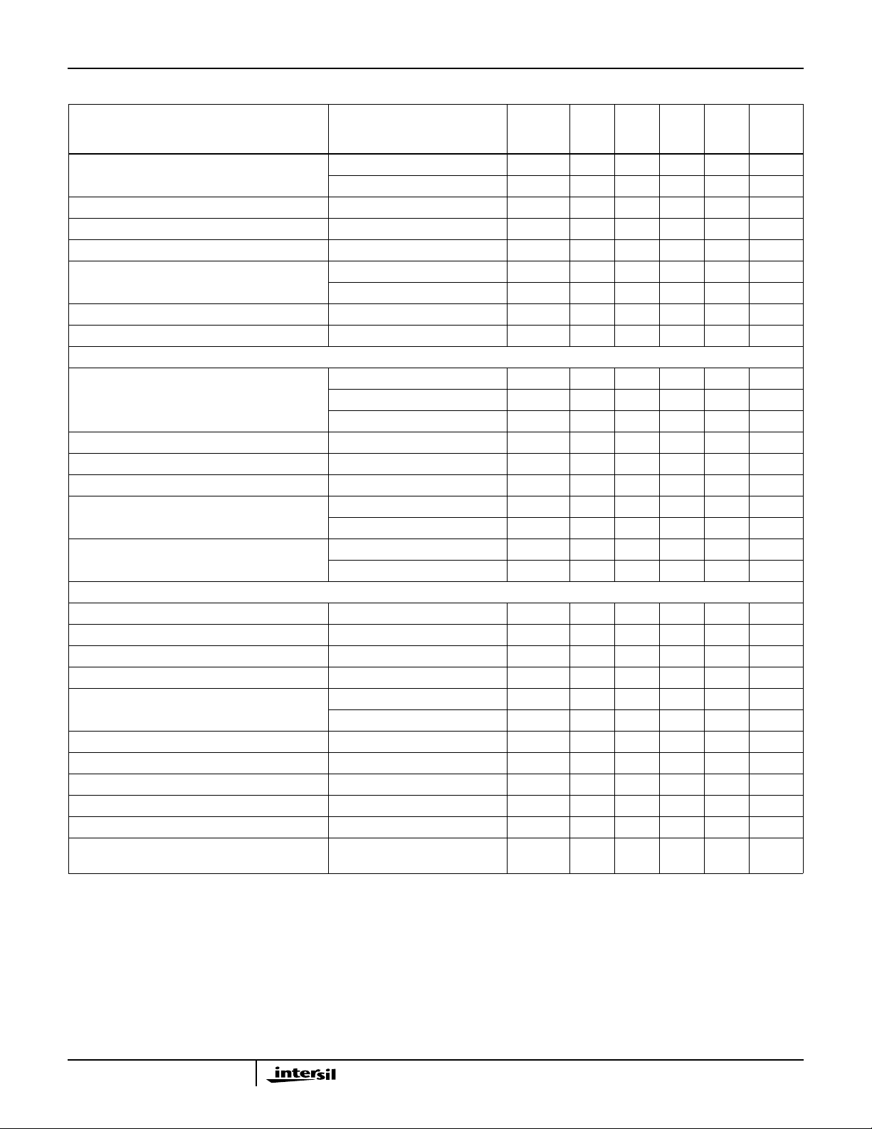
HA456
Electrical Specifications V
= ±5V, AGND = DGND = 0V, RL = 400Ω (Note 2), Unless Otherwise Specified. (Continued)
SUPPLY
(NOTE 3)
Output Capacitance
(Output Disabled)
PARAMETER TEST CONDITIONS
PLCC Package B 25 - 3.5 - pF
MQFP Package B 25 - 2.9 - pF
TEST
LEVEL
TEMP
(oC) MIN TYP MAX UNITS
Power Supply Rejection Ratio DC, VS= ±4.5V to±5.5V,VIN= 0V A Full 45 53 - dB
Digital Input Current (Note 5) VIN = 0V or 5V A Full - - 1 µA
Digital Input Low Voltage A Full - - 0.8 V
Digital Input High Voltage A 25 2.0 - - V
A Full 2.2 - - V
SER OUT Logic Low Voltage Serial Mode, IOL = 1.6mA A Full - - 0.4 V
SER OUT Logic High Voltage Serial Mode, IOH = -0.4mA A Full 3.0 - - V
AC CHARACTERISTICS (Note 4)
-3dB Bandwidth (Note 6) CL= 5pF, VIN = 200mV
CL = 5pF, VIN = 1V
CL = 5pF, VIN = 2V
Slew Rate (Note 6) V
OUT
= 4V
P-P
All Hostile Crosstalk (Note 6) 10MHz, VIN = 1V
All Hostile Off Isolation (Note 6) 10MHz, VIN = 1V
P-P
P-P
, RL=1kΩ B 25 - -55 - dB
P-P
P-P
P-P
B 25 - 120 - MHz
B 25 - 70 - MHz
B 25 - 50 - MHz
B 25 - 200 - V/µs
B 25 - 70 - dB
Differential Phase NTSC or PAL, RL= 1kΩ B 25 - 0.05 - DEG
NTSC or PAL, RL≥ 10kΩ B 25 - 0.05 - DEG
Differential Gain NTSC or PAL, RL= 1kΩ B 25 - 0.05 - %
NTSC or PAL, RL≥10kΩ B 25 - 0.02 - %
TIMING CHARACTERISTICS (See Figure 3 for more information)
Write Pulse Width High (tWH) A Full 20 - - ns
Write Pulse Width Low (tWL) A Full 20 - - ns
Chip-Enable Setup Time to Write (tCS) A Full 5 - - ns
Chip-Enable Hold Time From Write (tCH) A Full 5 - - ns
Data and Address Setup Time to Write (tDS) Parallel Mode A Full 20 - - ns
Serial Mode A Full 20 - - ns
Data and Address Hold Time From Write (tDH) A Full 25 - - ns
Latch Pulse Width (tL) A Full 40 - - ns
Latch Delay From Write (tD) A Full 40 - - ns
LATCH Edge to Output Disabled (t
) Serial Mode B Full - 30 - ns
OFF
LATCH Edge to Output Enabled (tON) Serial Mode B Full - 185 - ns
Output Break-Before-Make Delay
(t
ON -tOFF
)
Serial Mode B Full - 155 - ns
NOTES:
2. For the lowest crosstalk, and the best composite video performance, use RL≥ 1kΩ.
3. Test Level: A. Production Tested; B. Typical or Guaranteed Limit Based on Characterization; C. Design Typical for Information Only.
4. See AC Test Circuits (Figure 6 through Figure 9).
5. Excludes D1/SER OUT which is a bidirectional terminal and thus falls under the higher Output Leakage limit.
6. See Typical Performance Curves for more information.
5
 Loading...