Intersil Corporation HA4344B Datasheet

June 1998
HA4344B
350MHz, 4 x 1 Video Crosspoint Switch
with Synchronous Controls
Features
• Low Power Dissipation . . . . . . . . . . . . . . . . . . . 105mW
• Symmetrical Slew Rates . . . . . . . . . . . . . . . . . 1400V/µs
• 0.1dB Gain Flatness. . . . . . . . . . . . . . . . . . . . . . 100MHz
• -3dB Bandwidth . . . . . . . . . . . . . . . . . . . . . . . . . 350MHz
• Off Isolation (100MHz). . . . . . . . . . . . . . . . . . . . . . 70dB
• Crosstalk Rejection (30MHz). . . . . . . . . . . . . . . . . 80dB
• Differential Gain and Phase . . . . . 0.01%/0.01Degrees
• High ESD Rating . . . . . . . . . . . . . . . . . . . . . . . . >2000V
• TTL Compatible Control Signals
• Latched Control Lines for Synchronous Switching
Applications
• Professional Video Switching and Routing
• RGB Video Distribution Systems
• Computer Graphics
• RF Switching and Routing
Description
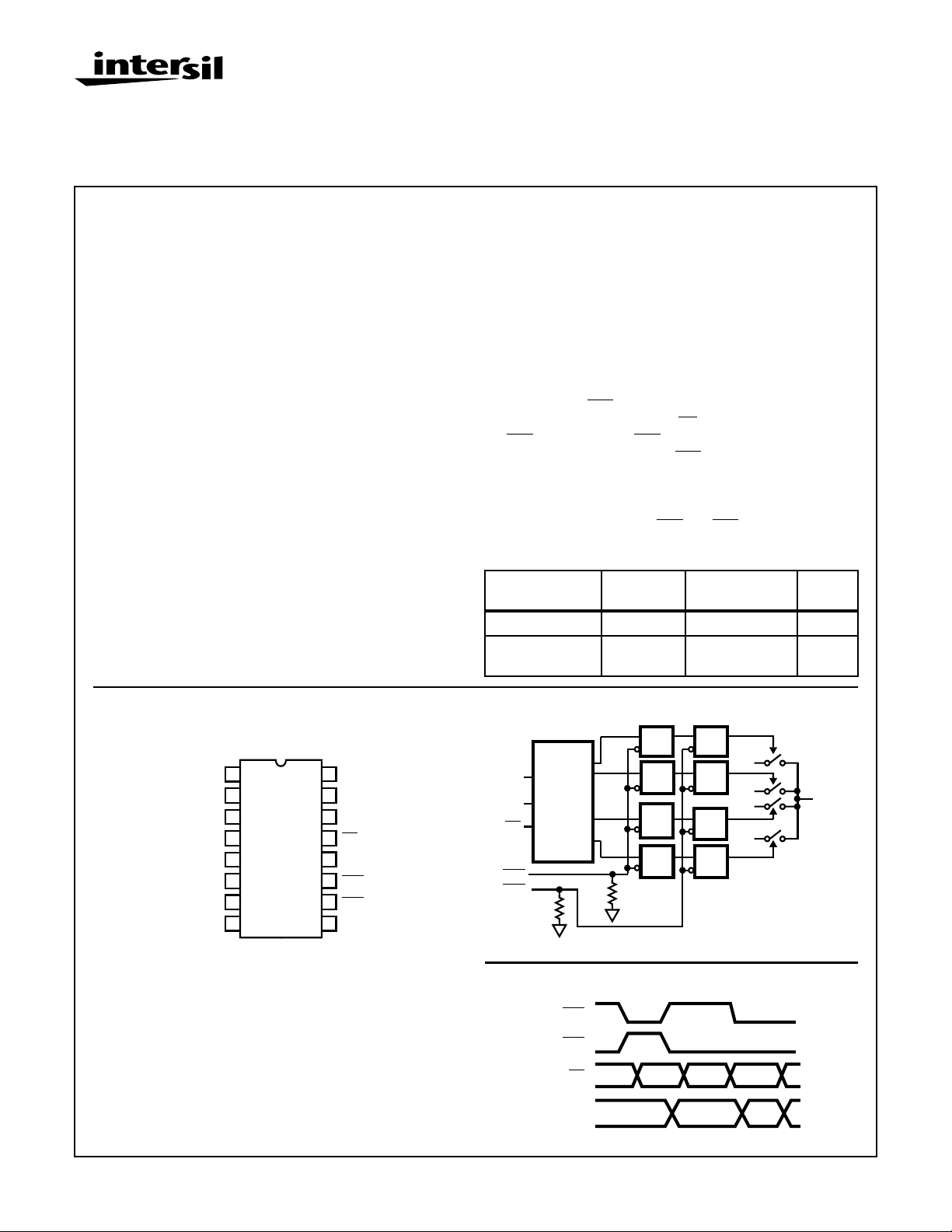
The HA4344B is a very wide bandwidth 4 x 1 crosspoint
switch ideal for professional video switching, HDTV, computer display routing, and other high performance applications. This circuit features very low power dissipation,
excellent differential gain and phase, high off isolation, symmetric slew rates, fast switching, and latched controlsignals.
When disabled, the output is switched to a high impedance
state, making the HA4344B ideal for matrix routers.
The latched control signals allow for synchronized channel
switching. When
next switching address (A0, A1,
ing
CK2 is the inverse of CK1) slave control latch maintains the
crosspoint in its current state.
CK1 is low the master control latch loads the
CS), while the closed (assum-
CK2 switching low closes the
master latch (with previous assumption), loads the now open
slave latch, and switches the crosspoint to the newly selected
channel. Channel selection is asynchronous (changes with any
control signal change) if both
CK1 and CK2 are low.
Ordering Information
TEMP.
PART NUMBER
HA4344BCB 0 to 70 16 Ld SOIC M16.15
HA4344BCB96 0 to 70 16 Ld SOIC Tape
RANGE (oC) PACKAGE
and Reel
PKG.
NO.
M16.15
Pinout
HA4344B (SOIC)
1
IN0
2
GND
3
IN1
GND
4
IN2
5
GND
6
7
IN3
8
GND
TOP VIEW
Functional Diagram
EN0
V+
16
15
A0
A1
14
13
CS
OUT
12
11
CK2
10
CK1
9
V-
A0
A1
CS
CK1
CK2
DECODE
100kΩ
EN1
EN2
EN3
100kΩ
Q
D
L
C
Q
D
L
C
Q
D
L
C
Q
D
L
C
Q
D
L
C
IN0
Q
D
L
C
IN1
IN2
Q
D
L
C
IN3
Q
D
L
C
OUT
Timing Diagram
CK1
CK2
A0, A1, CS
CHX CHY CHZ
OUT
CHX
CHX
CHY CHX
CHZ
CHZ
CAUTION: These devices are sensitive to electrostatic discharge. Users should follow proper IC Handling Procedures.
1-888-INTERSIL or 321-724-7143 | Copyright © Intersil Corporation 1999
1
File Number 3956.2

HA4344B
Absolute Maximum Ratings Thermal Information
Voltage Between V+ and V- . . . . . . . . . . . . . . . . . . . . . . . . . . . . 12V
Input Voltage. . . . . . . . . . . . . . . . . . . . . . . . . . . . . . . . . . . . V
Digital Input Current (Note 2) . . . . . . . . . . . . . . . . . . . . . . . . ±25mA
Analog Input Current (Note 2) . . . . . . . . . . . . . . . . . . . . . . . . ±5mA
Output Current . . . . . . . . . . . . . . . . . . . . . . . . . . . . . . . . . . . . 20mA
ESD Rating
Human Body Model (Per MIL-STD-883 Method 3015.7) . . 2000V
SUPPLY
Operating Conditions
Temperature Range . . . . . . . . . . . . . . . . . . . . . . . . . . . 0oC to 70oC
CAUTION: Stresses above those listed in “Absolute Maximum Ratings” may cause permanent damage to the device. This is a stress only rating and operation
of the device at these or any other conditions above those indicated in the operational sections of this specification is not implied.
NOTES:
1. θJA is measured with the component mounted on an evaluation PC board in free air.
2. If an input signal is applied before the supplies are powered up, the input current must be limited to these maximum values.
Thermal Resistance (Typical, Note 1) θJA (oC/W)
SOIC Package. . . . . . . . . . . . . . . . . . . . . . . . . . . . . 115
Maximum Junction Temperature (Die). . . . . . . . . . . . . . . . . . . . 175oC
Maximum Junction Temperature (Plastic Package) . . . . . . . .150oC
Maximum Storage Temperature Range . . . . . . . . . -65oC to 150oC
Maximum Lead Temperature (Soldering 10s) . . . . . . . . . . . . 300oC
(SOIC - Lead Tips Only)
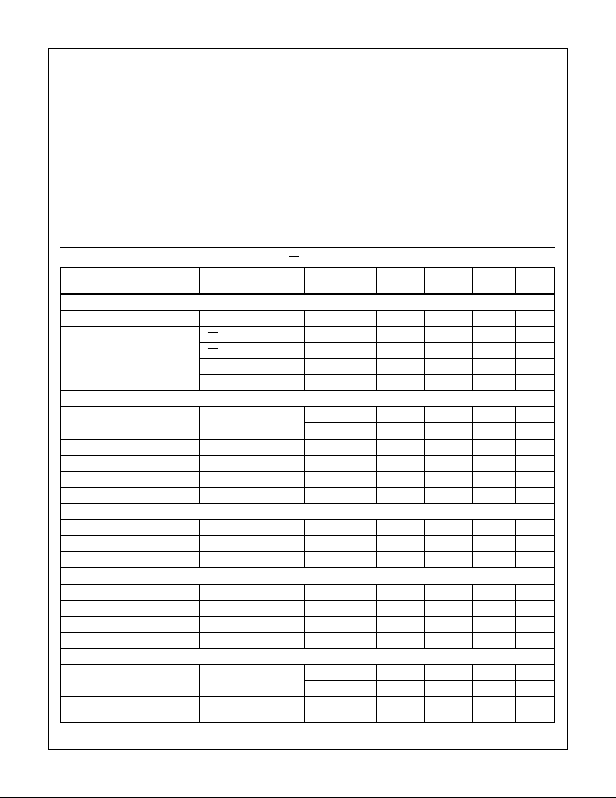
Electrical Specifications V
PARAMETER TEST CONDITIONS
DC SUPPLY CHARACTERISTICS
Supply Voltage Full ±4.5 ±5.0 ±5.5 V
Supply Current (V
ANALOG DC CHARACTERISTICS
Output Voltage Swing Without
Clipping
Output Current Full 15 20 - mA
Input Bias Current Full - 30 50 µA
Output Offset Voltage Full -10 - 10 mV
Output Offset Voltage Drift (Note 3) Full - 25 50 µV/°C
SWITCHING CHARACTERISTICS
Turn-On Time 25 - 160 - ns
Turn-Off Time 25 - 320 - ns
Output Glitch During Switching 25 - ±10 - mV
DIGITAL DC CHARACTERISTICS
Input Logic High Voltage Full 2 - - V
Input Logic Low Voltage Full - - 0.8 V
CLK1, CLK2 Input Current 0 to 4V Full - 40 50 µA
CS, A0, A1 Input Current 0 to 4V Full -2 - 2 µA
AC CHARACTERISTICS
Insertion Loss 1V
Channel-to-Channel Insertion Loss
Match
= 0V) VCS= 0.8V 25, 70 - 10.5 13 mA
OUT
= ±5V, RL = 10kΩ, VCS= 0.8V, Unless Otherwise Specified
SUPPLY
(NOTE 4)
TEMP. (oC) MIN TYP MAX UNITS
VCS= 0.8V 0 - - 15.5 mA
VCS= 2.0V 25, 70 - 400 450 µA
VCS= 2.0V 0 - 400 580 µA
V
= VIN ±VIO ±20mV 25, 70 ±2.7 ±2.8 - V
OUT
0 ±2.4 ±2.5 - V
P-P
25 - 0.055 0.063 dB
Full - 0.07 0.08 dB
Full - ±0.004 ±0.006 dB
2
 Loading...