

®
HA4314B
Data Sheet September 11, 2007 FN3679.12
400MHz, 4x1 Video Crosspoint Switch
The HA4314B is a very wide bandwidth 4x1 crosspoint switch
ideal for professional video switching, HDTV, computer monitor
routing, and other high performance applications. The circuit
features very low power dissipation (105mW Enabled, 4mW
Disabled), excellent differential gain and phase, and very high
off isolation. When disabled, the output is switched to a high
impedance state, making the HA4314B ideal for routing matrix
equipment.
The HA4314B requires no external current source, and
features fast switching and symmetric slew rates.
For a 4x1 crosspoint with Tally outputs (channel indicators) or
with synchronous control signals, please refer to the HA4404B
and HA4344B data sheets, respectively .
For audio channels requiring larger signal swings, please refer
to the CD22M3494 (16x8) data sheet.
Ordering Information
TEMP.
PART
NUMBER
HA4314BCA HA 4314BCA 0 to +70 16 Ld QSOP M16.15A
HA4314BCAZ*
(Note)
HA4314BCB* HA4314BCB 0 to +70 14 Ld SOIC M14.15
HA4314BCBZ*
(Note)
HA4314BCP HA4314BCP 0 to +70 14 Ld PDIP E14.3
HA4314BCPZ
(Note)
*Add “96” suffix for tape and reel. Please refer to TB347 for details on
reel specifications.
**Pb-free PDIPs can be used for through hole wave solder
processing only. They are not intended for use in Reflow solder
processing applications
NOTE: These Intersil Pb-free plastic packaged products employ
special Pb-free material sets; molding compounds/die attach
materials and 100% matte tin plate PLUS ANNEAL - e3 termination
finish, which is RoHS compliant and compatible with both SnPb and
Pb-free soldering operations. Intersil Pb-free products are MSL
classified at Pb-free peak reflow temperatures that meet or exceed
the Pb-free requirements of IPC/JEDEC J STD-020.
PART
MARKING
HA43 14BCAZ 0 to +70 16 Ld QSOP
4314BCBZ 0 to +70 14 Ld SOIC
HA4314BCPZ 0 to +70 14 Ld PDIP**
RANGE
(°C) PACKAGE
(Pb-free)
(Pb-free)
(Pb-free)
PKG.
DWG. #
M16.15A
M14.15
E14.3
Features
• Low Power Dissipation. . . . . . . . . . . . . . . . . . . . . . . . 105mW
• Symmetrical Slew Rates. . . . . . . . . . . . . . . . . . . . . 1400V/μs
• 0.1dB Gain Flatness. . . . . . . . . . . . . . . . . . . . . . . . . 100MHz
• -3dB Bandwidth. . . . . . . . . . . . . . . . . . . . . . . . . . . . . 400MHz
• Off Isolation (100MHz) . . . . . . . . . . . . . . . . . . . . . . . . . . 70dB
• Crosstalk Rejection (30MHz) . . . . . . . . . . . . . . . . . . . . . 80dB
• Differential Gain and Phase . . . . . . . . . . . . . . . 0.01%/0.01 °
• High ESD Rating. . . . . . . . . . . . . . . . . . . . . . . . . . . . . >2000V
• TTL Compatible Control Inputs
• Improved Replacement for GX4314 and GX4314L
• Pb-Free Available (RoHS Compliant)
Applications
• Professional Video Switching and Routing
• HDTV
• Computer Graphics
• RF Switching and Routing
• PCM Data Routing
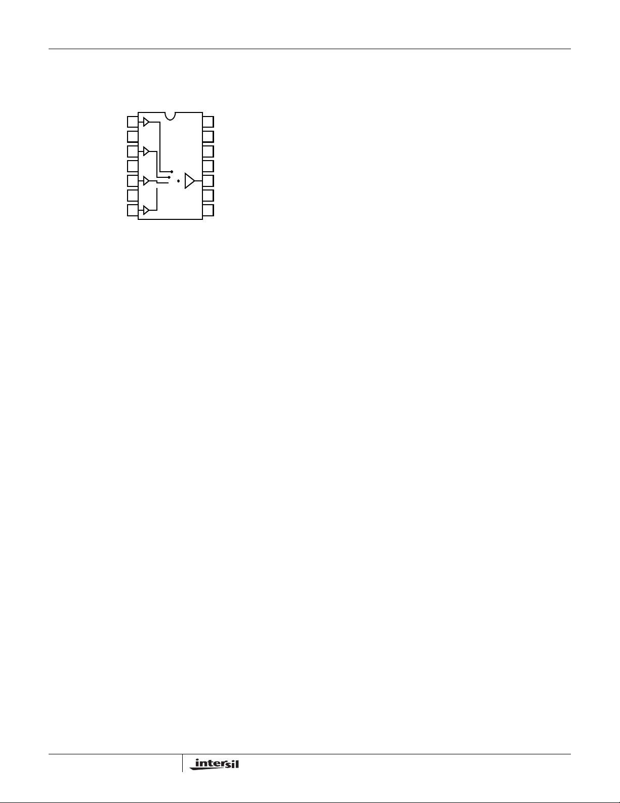
Truth Table
CS A1 A0 OUT
000IN0
001IN1
010IN2
011IN3
1XXHIGH-Z
1
CAUTION: These devices are sensitive to electrostatic discharge; follow proper IC Handling Procedures.
1-888-INTERSIL or 1-888-468-3774
| Intersil (and design) is a registered trademark of Intersil Americas Inc.
Copyright Intersil Americas Inc. 2004, 2006, 2007. All Rights Reserved
All other trademarks mentioned are the property of their respective owners.
T
Pinouts
HA4314B
(14 LD SOIC, PDIP)
TOP VIEW
1
2
3
4
5
6
7
HA4314B
(16 LD QSOP)
TOP VIEW
V+
14
13
12
11
10
9
8
NOTE: These pins must be left floating or connected to ground
2
FN3679.12
September 11, 2007
HA4314B
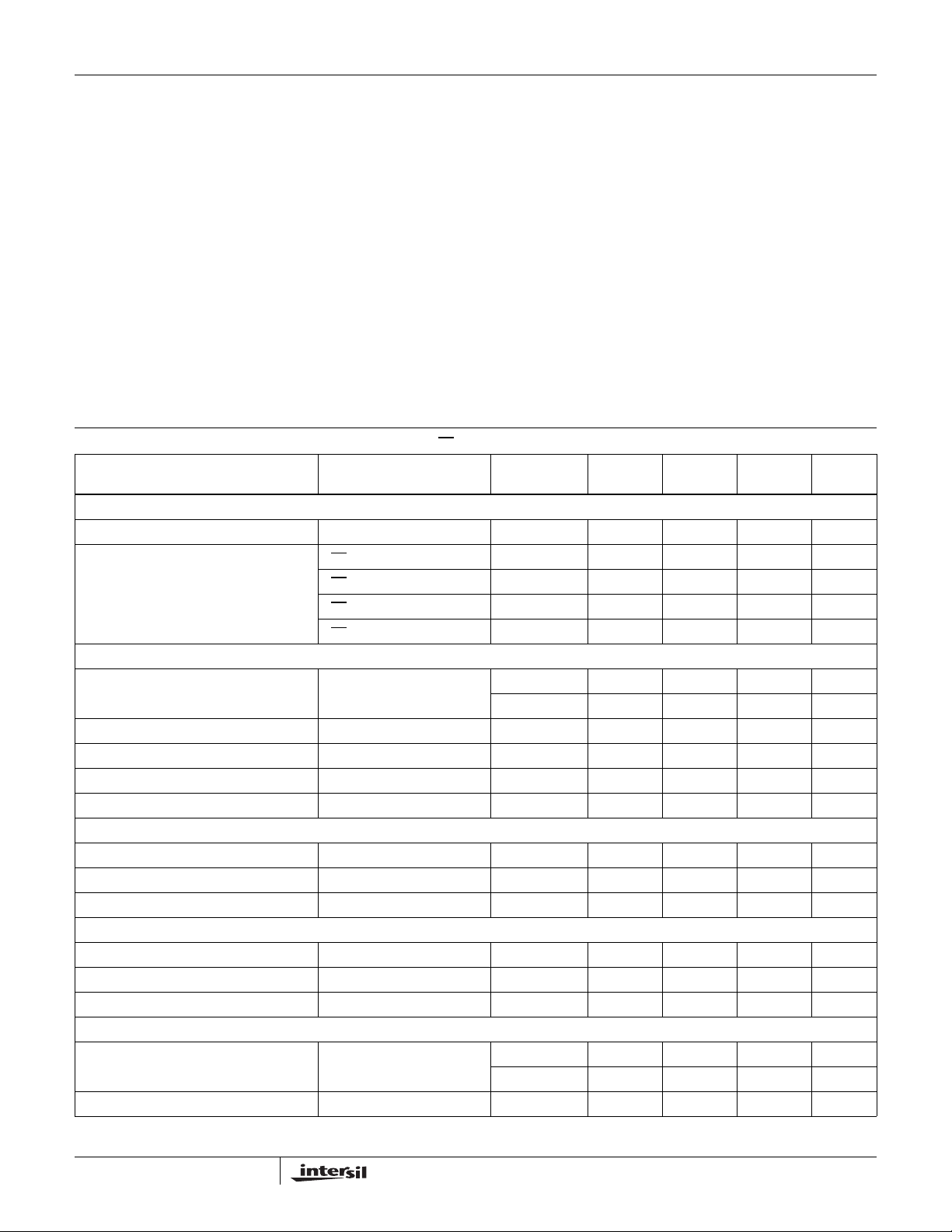
Absolute Maximum Ratings Thermal Information
Voltage Between V+ and V-. . . . . . . . . . . . . . . . . . . . . . . . . . . . 12V
Input Voltage . . . . . . . . . . . . . . . . . . . . . . . . . . . . . . . . . . . V
SUPPLY
Digital Input Current (Note 2). . . . . . . . . . . . . . . . . . . . . . . . . ±25mA
Analog Input Current (Note 2) . . . . . . . . . . . . . . . . . . . . . . . . . ±5mA
Output Current. . . . . . . . . . . . . . . . . . . . . . . . . . . . . . . . . . . . . 20mA
ESD Rating
Human Body Model (Per MIL-STD-883 Method 3015.7). . . .2000V
Operating Conditions
Temperature Range. . . . . . . . . . . . . . . . . . . . . . . . . . . 0°C to +70°C
CAUTION: Do not operate at or near the maximum ratings listed for extended periods of time. Exposure to such conditions may adversely impact product reliability and
result in failures not covered by warranty.
NOTES:
is measured with the component mounted on a low effective thermal conductivity test board in free air. See Tech Brief TB379 for details.
1. θ
JA
2. If an input signal is applied before the supplies are powered up, the input current must be limited to these maximum values.
Thermal Resistance (Typical, Note 1)
θ
JA
(°C/W)
14 Ld PDIP Package* . . . . . . . . . . . . . . . . . . . . . . . 95
14 Ld SOIC Package . . . . . . . . . . . . . . . . . . . . . . . . 120
16 Ld QSOP Package . . . . . . . . . . . . . . . . . . . . . . . 140
Maximum Junction Temperature (Die). . . . . . . . . . . . . . . . . . +175°C
Maximum Junction Temperature (Plastic Package) . . . . . . +150°C
Maximum Storage Temperature Range. . . . . . . . . -65°C to +150°C
Pb-free reflow profile . . . . . . . . . . . . . . . . . . . . . . . . . .see link below
http://www.intersil.com/pbfree/Pb-FreeReflow.asp
*Pb-free PDIPs can be used for through hole wave solder
processing only. They are not intended for use in Reflow solder
processing applications.
Electrical Specifications V
PARAMETER TEST CONDITIONS TEMP. (°C)
= ±5V, RL = 10kΩ, VCS= 0.8V, Unless Otherwise Specified.
SUPPLY
MIN
(Note 4) TYP
MAX
(Note 4) UNITS
DC SUPPLY CHARACTERISTICS
Supply Voltage Full ±4.5 ±5.0 ±5.5 V
Supply Current (V
=0V) VCS= 0.8V 25, 70 - 10.5 13 mA
OUT
VCS= 0.8V 0 - - 15.5 mA
V
= 2.0V 25, 70 - 400 450 µA
CS
V
= 2.0V 0 - 400 580 µA
CS
ANALOG DC CHARACTERISTICS
Output Voltage Swing without Clipping V
OUT=VIN
± VIO± 20mV 25, 70 ±2.7 ±2.8 -V
0±2.4±2.5 -V
Output Current Full 15 20 - mA
Input Bias Current Full - 30 50 µA
Output Offset Voltage Full -10 - 10 mV
Output Offset Voltage Drift (Note 3) Full - 25 50 µV/°C
SWITCHING CHARACTERISTICS
Turn-On Time 25 - 160 - ns
Turn-Off Time 25 - 320 - ns
Output Glitch During Switching 25 - ±10 - mV
DIGITAL DC CHARACTERISTICS
Input Logic High Voltage Full 2 - - V
Input Logic Low Voltage Full - - 0.8 V
Input Current 0V to 4V Full -2 - 2 µA
AC CHARACTERISTICS
Insertion Loss 1V
P-P
25 - 0.055 0.063 dB
Full - 0.07 0.08 dB
Channel-to-Channel Insertion Loss Match Full - ±0.004 ±0.006 dB
3
FN3679.12
September 11, 2007
HA4314B
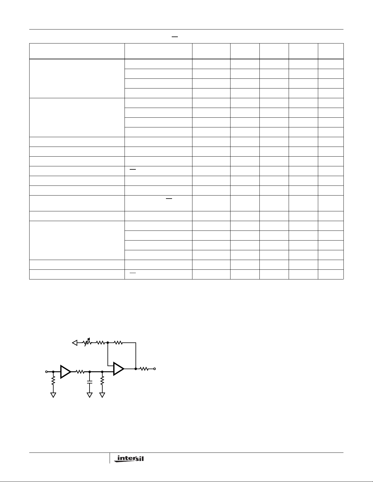
Electrical Specifications V
PARAMETER TEST CONDITIONS TEMP. (°C)
= ±5V, RL = 10kΩ, VCS= 0.8V, Unless Otherwise Specified. (Continued)
SUPPLY
MIN
(Note 4) TYP
MAX
(Note 4) UNITS
-3dB Bandwidth RS=50Ω, CL= 10pF 25 - 400 - MHz
=20Ω, CL= 20pF 25 - 280 - MHz
R
S
R
=16Ω, CL= 36pF 25 - 140 - MHz
S
R
=13Ω, CL= 49pF 25 - 110 - MHz
S
±0.1dB Flat Bandwidth RS=50Ω, CL= 10pF 25 - 100 - MHz
R
=20Ω, CL= 20pF 25 - 100 - MHz
S
R
=16Ω, CL= 36pF 25 - 85 - MHz
S
RS=13Ω, CL= 49pF 25 - 75 - MHz
Input Resistance Full 200 400 - kΩ
Input Capacitance Full - 1.5 - pF
Enabled Output Resistance Full - 15 - Ω
Disabled Output Capacitance V
= 2.0V Full - 2.5 - pF
CS
Differential Gain 4.43MHz, (Note 3) 25 - 0.01 0.02 %
Differential Phase 4.43MHz, (Note 3) 25 - 0.01 0.02 °
Off Isolation 1V
Crosstalk Rejection 1V
Slew Rate (1.5V
, +SR/-SR) RS=50Ω, CL= 10pF 25 - 1425/1450 - V/µs
P-P
, 100MHz, VCS=2.0V,
P-P
R
=10Ω
L
, 30MHz Full - 80 - dB
P-P
R
=20Ω, CL= 20pF 25 - 1010/1010 - V/µs
S
R
=16Ω, CL= 36pF 25 - 725/750 - V/µs
S
Full - 70 - dB
RS=13Ω, CL= 49pF 25 - 600/650 - V/µs
Total Harmonic Distortion 10MHz, R
Disabled Output Resistance V
CS
=1kΩ, (Note 3) Full - 0.01 0.1 %
L
= 2.0V Full - 12 - MΩ
NOTES:
3. Limits should be considered typical and are not production tested.
4. Parts are 100% tested at +25°C. Over-temperature limits established by characterization and are not production tested.
AC Test Circuit PC Board Layout
500Ω
400Ω 510Ω
HA4314
V
IN
75Ω
R
S
C
X
10kΩ
+
NOTE: CL = CX + Test Fixture Capacitance.
4
HFA1100
75Ω
V
OUT
The frequency response of this circuit depends greatly on
the care taken in designing the PC board. The use of low
inductance components such as chip resistors and chip
capacitors is strongly recommended, while a solid
ground plane is a must!
Attention should be given to decoupling the power supplies.
A large value (10µF) tantalum in parallel with a small value
(0.1µF) chip capacitor works well in most cases.
Keep input and output traces as short as possible, because
trace inductance and capacitance can easily become the
performance limiting items.
FN3679.12
September 11, 2007

Application Information
General
The HA4314B is a 4x1 crosspoint switch that is ideal for the
matrix element of high performance switchers and routers.
This crosspoint’s low input capacitance and high input
resistance provide excellent video terminations when used
with an external 75Ω resistor. Nevertheless, if several
HA4314B inputs are connected together, the use of an input
buffer should be considered (see Figure 1). This crosspoint
contains no feedback or gain setting resistors, so the output
is a true high impedance load when the IC is disabled
(CS
=1).
Ground Connections
All GND pins are connected to a common point on the die,
so any one of them will suffice as the functional GND
connection. For the best isolation and crosstalk rejection,
however, all GND pins must connect to the GND plane.
Frequency Response
Most applications utilizing the HA4314B require a series
output resistor, R
capacitance, C
as C
increases (as shown in the “Electrical Specifications”
L
on page 4), so give careful consideration to component
placement to minimize trace length. In big matrix
configurations where C
, to tune the response for the specific load
S
, driven. Bandwidth and slew rate degrade
L
is large, better frequency response
L
5
FN3679.12
September 11, 2007

HA4314B
SOURCE 0
SOURCE 1
SOURCE 2
SOURCE 3
INPUT BUFFERS
75Ω
75Ω
75Ω
75Ω
SOURCE0
SOURCE3
+5V
EN
OUT
HA4600
+5V
HA4600
R
S
EN
OUT
R
S
OUTPUT BUFFERS
(HFA1112 OR HFA1115)
IN0
IN1
75Ω
IN2
IN3
75Ω
SWITCH MATRIX
IN0
HA4314
IN3
CS
OUT
R
S
OUT0
+
-
X2
75Ω
IN0
HA4314
IN3
CS
OUT
R
S
OUT1
+
IN0
HA4314
OUT
IN3
-
X2
75Ω
FIGURE 1. 4x4 SWITCHER/ROUTER APPLICATION
HA4314
CS
OUT
SEL0:3
R
S
SEL4:7
1/4 CD74HCT00
EN
R
S
CS
R
S
OUT2
+
-
X2
75Ω
IN0
HA4314
IN3
CS
OUT
R
S
OUT3
+
-
X2
75Ω
SOURCE4
SOURCE7
SOURCE8
SOURCE11
SOURCE12
SOURCE15
75Ω
75Ω
75Ω
75Ω
75Ω
75Ω
OUT
IN0
IN1
IN2
CS
R
S
HA4201
IN3
SEL8:11
HA4314
SEL12:15
IN0
IN1
IN2
IN3
IN0
IN1
IN2
CS
OUT
OUT
CS
R
S
R
S
1/4 CD74HCT00
EN
HA4201
IN3
HA4314
SWITCHING
MATRIX
ISOLATION
MUX
FIGURE 2. 16x1 SWITCHER APPLICATION
HFA1112 OR HFA1115
-
+
R
S
75Ω
OUT
X2
OUTPUT
BUFFER
6
FN3679.12
September 11, 2007

Typical Performance Curves V
= ±5V, TA = +25°C, RL = 10kΩ, Unless Otherwise Specified
SUPPLY
1.00
0.75
0.50
0.25
0
-0.25
OUTPUT VOLTAGE (V)
-0.50
-0.75
-1.00
TIME (5ns/DIV)
FIGURE 3. LARGE SIGNAL PULSE RESPONSE
VIN = 1V
12
9
6
3
0
-3
GAIN (dB)
-6
-9
-12
P-P
CL = 20pF
= 36pF
C
L
= 49pF
C
L
CL = 10pF
IN1 = +250mV
2.4
1.6
A1 (V)
0.8
250
125
OUTPUT VOLTAGE (mV)
0
0
IN3 = 0V
A0 = +3V
TIME (200ns/DIV)
FIGURE 4. CHANNEL-TO-CHANNEL SWITCHING RESPONSE
VIN = 1V
0.4
0.3
0.2
0.1
0
-0.1
GAIN (dB)
-0.2
-0.3
-0.4
P-P
CL = 10pF
CL = 49pF
C
= 36pF
L
CL = 20pF
CL = 20pF
1M 10M 100M 500M
FREQUENCY (Hz)
FIGURE 5. FREQUENCY RESPONSE
VIN = 1V
P-P
RL = 10kΩ
-40
-50
-60
-70
-80
-90
CROSSTALK (dB)
-100
-110
-120
0.6M 1M 10M 100M 200M
FREQUENCY (Hz)
PDIP
SOIC
SSOP
1M 10M 100M 200M
FREQUENCY (Hz)
FIGURE 6. GAIN FLATNESS
FIGURE 7. ALL HOSTILE CROSSTALK REJECTION FIGURE 8. ALL HOSTILE OFF ISOLATION
7
FN3679.12
September 11, 2007

HA4314B
Typical Performance Curves V
0.20
VIN = 1V
P-P
RL = 1kΩ
0.15
0.10
0.05
TOTAL HARMONIC DISTORTION (%)
0
10M 20M 30M 40M 50M 60M 70M 80M 90M 100M
FREQUENCY (Hz)
= ±5V, TA = +25°C, RL = 10kΩ, Unless Otherwise Specified (Continued)
SUPPLY
3.4
3.2
3.0
2.8
2.6
2.4
2.2
2.0
INPUT CAPACITANCE (pF)
1.8
1.6
1.4
1M 10M 100M
CH 1
CH 2
FREQUENCY (Hz)
CH 3
FIGURE 9. TOTAL HARMONIC DISTORTION vs FREQUENCY FIGURE 10. INPUT CAPACITANCE vs FREQUENCY
35
30
25
CH 0
500M
20
15
NOISE (nV/√Hz)
10
5
0
1 10 100 1k 10k 100k
FREQUENCY (Hz)
FIGURE 11. NOISE vs FREQUENCY
8
FN3679.12
September 11, 2007

Die Characteristics
HA4314B
DIE DIMENSIONS:
65 milsx118 milsx19 mils
1640μmx3000μmx483μm
METALLIZATION:
Type: Metal 1: AlCu (1%)/TiW
Thickness: Metal 1: 6kÅ ±0.8kÅ
Type: Metal 2: AlCu (1%)
Thickness: Metal 2: 16k
Å ±1.1kÅ
Metallization Mask Layout
IN1
NC
HA4314B
IN0GND
PASSIVATION:
Type: Nitride
Thickness: 4kÅ ±0.5kÅ
TRANSISTOR COUNT:
200
SUBSTRATE POTENTIAL (POWERED UP):
V-
NC
V+
A0
A1
GND
NC
IN2
GND
IN3 V-NC
GND
CS
OUT
NC
NC
9
FN3679.12
September 11, 2007

Dual-In-Line Plastic Packages (PDIP)
HA4314B
N
D1
-C-
E1
-B-
A1
A2
E
A
L
e
C
C
L
e
A
C
e
B
INDEX
AREA
BASE
PLANE
SEATING
PLANE
D1
B1
12 3 N/2
-AD
e
B
0.010 (0.25) C AM BS
NOTES:
1. Controlling Dimensions: INCH. In case of conflict between English
and Metric dimensions, the inch dimensions control.
2. Dimensioning and tolerancing per ANSI Y14.5M-1982.
3. Symbols are defined in the “MO Series Symbol List” in Section 2.2 of
Publication No. 95.
4. Dimensions A, A1 and L are measured with the package seated in
JEDEC seating plane gauge GS-3.
5. D, D1, and E1 dimensions do not include mold flash or protrusions.
Mold flash or protrusions shall not exceed 0.010 inch (0.25mm).
6. E and are measured with the leads constrained to be
7. e
e
perpendicular to datum .
A
and eC are measured at the lead tips with the leads
B
unconstrained. e
-C-
must be zero or greater.
C
8. B1 maximum dimensions do not include dambar protrusions. Dambar
protrusions shall not exceed 0.010 inch (0.25mm).
9. N is the maximum number of terminal positions.
10. Corner leads (1, N, N/2 and N/2 + 1) for E8.3, E16.3, E18.3, E28.3,
E42.6 will have a B1 dimension of 0.030 - 0.045 inch (0.76 -
1.14mm).
E14.3 (JEDEC MS-001-AA ISSUE D)
14 LEAD DUAL-IN-LINE PLASTIC PACKAGE
INCHES MILLIMETERS
SYMBOL
A-0.210 - 5.33 4
A1 0.015 - 0.39 -4
A2 0.115 0.195 2.93 4.95 -
B 0.014 0.022 0.356 0.558 B1 0.045 0.070 1.15 1.77 8
C 0.008 0.014 0.204 0.355 -
D 0.735 0.775 18.66 19.68 5
D1 0.005 - 0.13 -5
E 0.300 0.325 7.62 8.25 6
E1 0.240 0.280 6.10 7.11 5
e 0.100 BSC 2.54 BSC e
A
e
B
0.300 BSC 7.62 BSC 6
- 0.430 - 10.92 7
L 0.115 0.150 2.93 3.81 4
N14 149
NOTESMIN MAX MIN MAX
Rev. 0 12/93
10
FN3679.12
September 11, 2007

Small Outline Plastic Packages (SOIC)
HA4314B
N
INDEX
AREA
123
-A-
E
-B-
SEATING PLANE
D
A
-C-
0.25(0.010) BM M
H
L
h x 45
o
α
e
B
0.25(0.010) C AM BS
M
NOTES:
1. Symbols are defined in the “MO Series Symbol List” in Section 2.2 of
Publication Number 95.
2. Dimensioning and tolerancing per ANSI Y14.5M-1982.
3. Dimension “D” does not include mold flash, protrusions or gate burrs.
Mold flash, protrusion and gate burrs shall not exceed 0.15mm (0.006
inch) per side.
4. Dimension “E” does not include interlead flash or protrusions. Interlead
flash and protrusions shall not exceed 0.25mm (0.010 inch) per side.
5. The chamfer on the body is optional. If it is not present, a visual index
feature must be located within the crosshatched area.
6. “L” is the length of terminal for soldering to a substrate.
7. “N” is the number of terminal positions.
8. Terminal numbers are shown for reference only.
9. The lead width “B”, as measured 0.36mm (0.014 inch) or greater
above the seating plane, shall not exceed a maximum value of
0.61mm (0.024 inch).
10. Controlling dimension: MILLIMETER. Converted inch dimensions
are not necessarily exact.
A1
C
0.10(0.004)
M14.15 (JEDEC MS-012-AB ISSUE C)
14 LEAD NARROW BODY SMALL OUTLINE PLASTIC
PACKAGE
INCHES MILLIMETERS
SYMBOL
A 0.0532 0.0688 1.35 1.75 -
A1 0.0040 0.0098 0.10 0.25 -
B 0.013 0.020 0.33 0.51 9
C 0.0075 0.0098 0.19 0.25 -
D 0.3367 0.3444 8.55 8.75 3
E 0.1497 0.1574 3.80 4.00 4
e 0.050 BSC 1.27 BSC -
H 0.2284 0.2440 5.80 6.20 -
h 0.0099 0.0196 0.25 0.50 5
L 0.016 0.050 0.40 1.27 6
N14 147
o
α
0
o
8
o
0
o
8
Rev. 0 12/93
NOTESMIN MAX MIN MAX
-
11
FN3679.12
September 11, 2007

HA4314B
Shrink Small Outline Plastic Packages (SSOP)
Quarter Size Outline Plastic Packages (QSOP)
N
INDEX
AREA
123
-AD
e
B
0.17(0.007) C AMB
H
E
-B-
SEATING PLANE
A
-C-
A1
S
M
0.25(0.010) B
GAUGE
PLANE
α
0.10(0.004)
M
0.25
0.010
A2
M
h x 45°
NOTES:
1. Symbols are defined in the “MO Series Symbol List” in Section
2.2 of Publication Number 95.
2. Dimensioning and tolerancing per ANSI Y14.5M-1982.
3. Dimension “D” does not include mold flash, protrusions or gate
burrs. Mold flash, protrusion and gate burrs shall not exceed
0.15mm (0.006 inch) per side.
4. Dimension “E” does not include interlead flash or protrusions.
Interlead flash and protrusions shall not exceed 0.25mm (0.010
inch) per side.
5. The chamfer on the body is optional. If it is not present, a visual
index feature must be located within the crosshatched area.
6. “L” is the length of terminal for soldering to a substrate.
7. “N” is the number of terminal positions.
8. Terminal numbers are shown for reference only.
9. Dimension “B” does not include dambar protrusion. Allowable
dambar protrusion shall be 0.10mm (0.004 inch) total in excess
of “B” dimension at maximum material condition.
10. Controlling dimension: INCHES. Converted millimeter dimensions are not necessarily exact.
M16.15A
16 LEAD SHRINK SMALL OUTLINE PLASTIC PACKAGE
(0.150” WIDE BODY)
INCHES MILLIMETERS
SYMBOL
A 0.061 0.068 1.55 1.73 -
A1 0.004 0.0098 0.102 0.249 -
L
A2 0.055 0.061 1.40 1.55 -
B 0.008 0.012 0.20 0.31 9
C 0.0075 0.0098 0.191 0.249 D 0.189 0.196 4.80 4.98 3
E 0.150 0.157 3.81 3.99 4
C
e 0.025 BSC 0.635 BSC H 0.230 0.244 5.84 6.20 h 0.010 0.016 0.25 0.41 5
L 0.016 0.035 0.41 0.89 6
N16 167
α
0° 8° 0° 8° -
NOTESMIN MAX MIN MAX
Rev. 2 6/04
All Intersil U.S. products are manufactured, assembled and tested utilizing ISO9000 quality systems.
Intersil Corporation’s quality certifications can be viewed at www.intersil.com/design/quality
Intersil products are sold by description only. Intersil Corporation reserves the right to make changes in circuit design, software and/or specifications at any time without
notice. Accordingly, the reader is cautioned to verify that data sheets are current before placing orders. Information furnished by Intersil is believed to be accurate and
reliable. However, no responsibility is assumed by Intersil or its subsidiaries for its use; nor for any infringements of patents or other rights of third parties which may result
from its use. No license is granted by implicat ion or oth erwise u nde r any p a tent or p at ent r ights of Intersil or its subsidiaries.
For information regarding Intersil Corporation and its products, see www.intersil.com
12
FN3679.12
September 11, 2007
 Loading...