1
File Number 2900.4
CAUTION: These devices are sensitive to electrostatic discharge; follow proper IC Handling Procedures.
1-888-INTERSIL or 321-724-7143
| Copyright © Intersil Corporation 1999
HA-2544
50MHz, Video Operational Amplifier
The HA-2544 is a fast, unity gain stable, monolithic op amp
designed to meet the needs required for accurate
reproduction of video or high speed signals. It offers high
voltage gain (6kV/V) and high phase margin (65 degrees)
while maintaining tight gain flatness over the video
bandwidth. Built from high quality Dielectric Isolation, the
HA-2544 is another addition to the Intersil series of high
speed, wideband op amps, and offers true video
performance combined with the versatility of an op amp.
The primary features of the HA-2544 include 50MHz Gain
Bandwidth, 150V/µs slew rate, 0.03% differential gain error
and gain flatness of just 0.12dB at 10MHz. High
performance and low power requirements are met with a
supply current of only 10mA.
Uses of the HA-2544 range from video test equipment,
guidance systems, radar displaysandotherpreciseimaging
systems where stringent gain and phase requirements have
previously been met with costly hybrids and discrete
circuitry. The HA-2544 will also be used in non-video
systems requiring high speed signal conditioning such as
data acquisition systems, medical electronics, specialized
instrumentation and communication systems.
Military (/883) product and data sheets are available upon
request.
Features
• Gain Bandwidth . . . . . . . . . . . . . . . . . . . . . . . . . . . 50MHz
• High Slew Rate. . . . . . . . . . . . . . . . . . . . . . . . . . . 150V/µs
• Low Supply Current . . . . . . . . . . . . . . . . . . . . . . . . . 10mA
• Differential Gain Error. . . . . . . . . . . . . . . . . . . . . . . 0.03%
• Differential Phase Error . . . . . . . . . . . . . . . . 0.03 Degrees
• Gain Flatness at 10MHz. . . . . . . . . . . . . . . . . . . . . 0.12dB
Applications
• Video Systems • Imaging Systems
• Video Test Equipment • Pulse Amplifiers
• Radar Displays • Signal Conditioning Circuits
• Data Acquisition Systems
Pinout
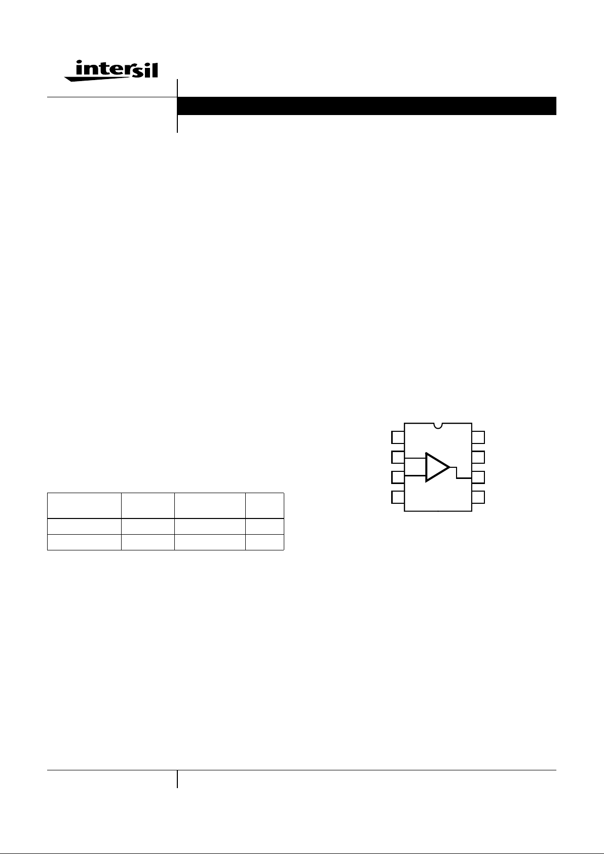
HA-2544 (CERDIP)
HA-2544C (PDIP)
TOP VIEW
Ordering Information
PART NUMBER
(BRAND)
TEMP.
RANGE (oC) PACKAGE
PKG.
NO.
HA3-2544C-5 0 to 75 8 Ld PDIP E8.3
HA7-2544-2 -55 to 125 8 Ld CERDIP F8.3A
1
2
3
4
8
7
6
5
NC
V+
OUT
BAL
BAL
-IN
+IN
V-
+
-
Data Sheet April 1999

2
Absolute Maximum Ratings Thermal Information
Voltage Between V+ and V- Terminals. . . . . . . . . . . . . . . . . . . . 35V
Differential Input Voltage (Note 1) . . . . . . . . . . . . . . . . . . . . . . . . 6V
Peak Output Current . . . . . . . . . . . . . . . . . . . . . . . . . . . . . . . ±40mA
Operating Conditions
Temperature Range
HA-2544C-5 . . . . . . . . . . . . . . . . . . . . . . . . . . . . . . . 0oC to 75oC
HA-2544-2 . . . . . . . . . . . . . . . . . . . . . . . . . . . . . . -55oC to 125oC
Thermal Resistance (Typical, Note 2) θJA (oC/W) θJC (oC/W)
PDIP Package . . . . . . . . . . . . . . . . . . . 92 N/A
CERDIP Package. . . . . . . . . . . . . . . . . 135 50
Maximum Junction Temperature (Hermetic Packages) . . . . . 175oC
Maximum Junction Temperature (Plastic Packages). . . . . . . 150oC
Maximum Storage Temperature Range. . . . . . . . . . -65oC to 150oC
Maximum Lead Temperature (Soldering 10s) . . . . . . . . . . . . 300oC
CAUTION: Stresses above those listed in “Absolute Maximum Ratings” may cause permanent damage to the device. This is a stress only rating and operation of the
device at these or any other conditions above those indicated in the operational sections of this specification is not implied.
NOTES:
1. To achieve optimum AC performance, the input stagewas designedwithout protective diode clamps. Exceeding the maximum differential input
voltage results in reverse breakdown of the base-emitter junction of the input transistors and probable degradation of the input parameters
especially VOS, IOS and Noise.
2. θJA is measured with the component mounted on an evaluation PC board in free air.
Electrical Specifications V
SUPPLY
= ±15V, CL≤10pF, RL = 1kΩ, Unless Otherwise Specified
PARAMETER
TEST
CONDITIONS
TEMP
(oC)
HA-2544-2 HA-2544C-5
UNITSMIN TYP MAX MIN TYP MAX
INPUT CHARACTERISTICS
Offset Voltage 25 - 6 15 - 15 25 mV
-2, -5 - - 20 - - 40 mV
-9 - - 25 - - 40 mV
Average Offset Voltage Drift (Note 7) Full - 10 - - 10 - µV/oC
Bias Current 25 - 7 15 - 9 18 µA
Full - - 20 - - 30 µA
Average Bias Current Drift (Note 7) Full - 0.04 - - 0.04 - µA/oC
Offset Current 25 - 0.2 2 - 0.8 2 µA
Full - - 3 - - 3 µA
Offset Current Drift Full - 10 - - 10 - nA/oC
Common Mode Range Full ±10 ±11.5 - ±10 ±11.5 - V
Differential Input Resistance 25 50 90 - 50 90 - kΩ
Differential Input Capacitance 25 - 3 - - 3 - pF
Input Noise Voltage f = 1kHz 25 - 20 - - 20 - nV/√Hz
Input Noise Current f = 1kHz 25 - 2.4 - - 2.4 - pA/√Hz
Input Noise Voltage (Note 7) 0.1Hz to 10Hz 25 - 1.5 - - 1.5 - µV
P-P
0.1Hz to 1MHz 25 - 4.6 - - 4.6 - µV
RMS
TRANSFER CHARACTERISTICS
Large Signal Voltage Gain (Note 7) VO = ±5V 25 3.5 6 - 3 6 - kV/V
Full 2.5 - - 2 - - kV/V
Common Mode Rejection Ratio (Note 7) ∆VCM = ±10V -2, -5 75 89 - 70 89 - dB
-9 75 89 - 65 89 - dB
Minimum Stable Gain 25 +1 - - +1 - - V/V
Unity Gain Bandwidth (Note 7) VO = ±100mV 25 - 45 - - 45 - MHz
Gain Bandwidth Product (Note 7) VO = ±100mV 25 - 50 - - 50 - MHz
HA-2544

3
Phase Margin 25 - 65 - - 65 - Degrees
OUTPUT CHARACTERISTICS
Output Voltage Swing
Full Power Bandwidth (Note 6)
Full ±10 ±11 - ±10 ±11 - V
25 3.2 4.2 - 3.2 4.2 - MHz
Peak Output Current (Note 7) 25 ±25 ±35 - ±25 ±35 - mA
Continuous Output Current (Note 7) 25 ±10 - - ±10 - - mA
Output Resistance Open Loop 25 - 20 - - 20 - Ω
TRANSIENT RESPONSE
Rise Time (Note 4) 25 - 7 - - 7 - ns
Overshoot (Note 4) 25 - 10 - - 10 - %
Slew Rate 25 100 150 - 100 150 - V/µs
Settling Time (Note 5) 25 - 120 - - 120 - ns
VIDEO PARAMETERS RL = 1kΩ (Note 8)
Differential Phase (Note 9) 25 - 0.03 - - 0.03 - Degree
Differential Gain (Notes 3, 9) 25 - 0.0026 - - 0.0026 - dB
25 - 0.03 - - 0.03 - %
Gain Flatness 5MHz 25 - 0.10 - - 0.10 - dB
10MHz 25 - 0.12 - - 0.12 - dB
Chrominance to Luminance Gain (Note 10) 25 - 0.1 - - 0.1 - dB
Chrominance to Luminance Delay (Note 10) 25 - 7 - - 7 - ns
POWER SUPPLY CHARACTERISTICS
Supply Current Full - 10 12 - 10 15 mA
Power Supply Rejection Ratio (Note 7) VS = ±10V to ±20V -2, -5 70 80 - 70 80 - dB
-9 65 80 - 65 80 - dB
NOTES:
3. .
4. For Rise Time and Overshoot testing, V
OUT
is measured from 0 to +200mV and 0 to -200mV.
5. Settling Time is specified to 0.1% of final value for a 10V step and AV = -1.
6. Full Power Bandwidth is guaranteed by equation: .
7. Refer to typical performance curve in Data Sheet.
8. The video parameter specifications will degrade as the output load resistance decreases.
9. Tested with a VM700A video tester, using aNTC-7 Compositeinput signal. For adequate test repeatability, aminimum warm-upof 2 minutes is
suggested. AV = +1.
10. C-L Gain and C-L Delay was less than the resolution of the test equipment used which is 0.1dB and 7ns, respectively.
Electrical Specifications V
SUPPLY
= ±15V, CL≤10pF, RL = 1kΩ, Unless Otherwise Specified (Continued)
PARAMETER
TEST
CONDITIONS
TEMP
(oC)
HA-2544-2 HA-2544C-5
UNITSMIN TYP MAX MIN TYP MAX
AD(%) 10
ADdB()
20
---------------------
1– 100×=
Full Power Bandwidth
Slew Rate
2π V
PEAK
---------------------------- -
V
PEAK
5V=()=
HA-2544

4
Test Circuits and Waveforms
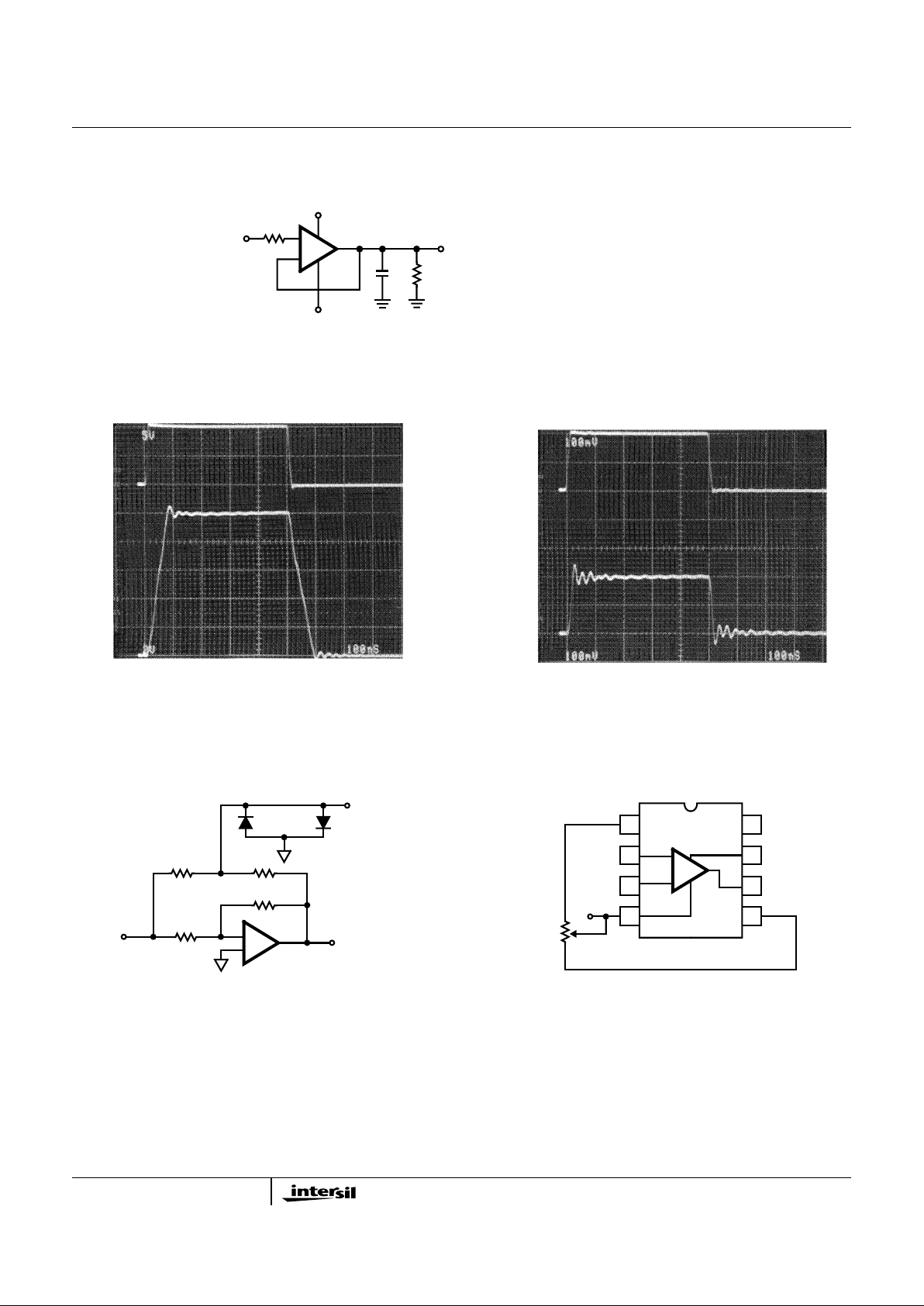
FIGURE 1. TRANSIENT RESPONSE
LARGE SIGNAL RESPONSE SMALL SIGNAL RESPONSE
FIGURE 2. SETTLING TIME TEST CIRCUIT FIGURE 3. OFFSET VOLTAGE ADJUSTMENT
R
L
V
OUT
V
IN
C
L
+
V-
V+
NOTES:
11. VS = ±15V.
12. AV = +1.
13. RS = 50Ω or 75Ω (Optional).
14. RL = 1kΩ.
15. CL < 10pF.
16. VIN for Large Signal = ±5V.
17. VINfor Small Signal =0 to
+200mV and 0 to -200mV.
R
S
-
V
IN
V
OUT
V
OUT
= 0 to +10V
Vertical Scale: VIN = 5V/Div.; V
OUT
= 2V/Div.
Horizontal Scale: 100ns/Div.
V
IN
V
OUT
V
OUT
= 0 to +200mV
Vertical Scale: VIN = 100mV/Div.; V
OUT
= 100mV/Div.
Horizontal Scale: 100ns/Div.
+
V
OUT
V
IN
SETTLING
POINT
5kΩ
2kΩ
2kΩ
5kΩ
NOTES:
18. AV = -1.
19. Feedbackand summingresistor ratiosshould be0.1% matched.
20. HP5082-2810 clipping diodes recommended.
21. Tektronix P6201 FET probe used at settling point.
-
1
2
3
8
7
6
5
NC
V+
OUT
BAL
BAL
-IN
+IN
V-
+
4
R
T
NOTE: Tested offset adjustment range is |VOS + 1mV| minimum
referred to output. Typical range for RT = 20kΩ is approximately
±30mV.
-
HA-2544
 Loading...