Intersil Corporation HA-2839-883 Datasheet

July 1994
HA-2839/883
Very High Slew Rate,
Wideband Operational Amplifier
Features
• This Circuit is Processed in Accordance to MIL-STD883 and is Fully Conformant Under the Provisions of
Paragraph 1.2.1.
• Supply Current. . . . . . . . . . . . . . . . . . . . . 15.0mA (Max)
• Low Offset Voltage. . . . . . . . . . . . . . . . . . . 2.0mV (Max)
• Very High Slew Rate . . . . . . . . . . . . . . . . 600V/µs (Typ)
• Open Loop Gain. . . . . . . . . . . . . . . . . . . . . 20kV/V (Min)
• Wide Gain-Bandwidth (A
• Input Noise Voltage at 1kHz . . . . . . . . . . 6nV/√
≥ 10) . . . . . . . 600MHz (Typ)
V
Hz (Typ)
• Enhanced Replacement for HA-2539/883 and EL2039
Applications
• Pulse and Video Amplifiers
• Wideband Amplifiers
• RF/IF Signal Processing
• High Speed Sample-Hold Circuits
• Fast, Precise D/A Converters
• RF Oscillators
Description
The HA-2839/883 is a wideband, very high slew rate, operational amplifier featuring superior speed and bandwidth
characteristics. It also features trimmed supply current,
which minimizes supply current (and thus A.C. parameter)
variation over process and temperature extremes. For example, the I
variation over the entire military temperature
CC
range is typically less than 0.5mA. Bipolar construction, coupled with dielectric isolation, delivers outstanding performance in circuits with closed loop gains ≥10.
The 600V/µs slew rate, and 600MHz gain bandwidth product
ensure high performance in video and wideband amplifier
designs. Differential gain and phase are a low 0.03% and
0.03 degrees, respectively, making the HA-2839/883 ideal
for video applications. A full ±10V output swing, high open
loop gain, and outstanding A.C. parameters make
the HA-2839/883 an excellent choice for data acquisition
systems.
Ordering Information
PART
NUMBER
HA1-2839/883 -55oC to +125oC 14 Lead CerDIP
TEMPERATURE
RANGE PACKAGE
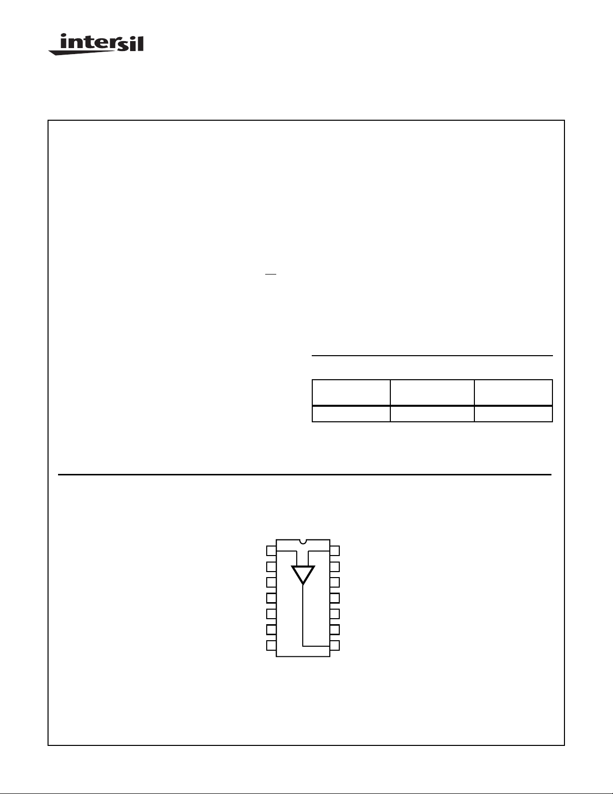
Pinout
HA-2839/883
(CERDIP)
TOP VIEW
+IN
1
2
NC
VNC
NC
NC
NC
CAUTION: These devices are sensitive to electrostatic discharge; follow proper IC Handling Procedures.
http://www.intersil.com
| Copyright © Intersil Corporation 1999
+-
3
4
5
6
7
3-53
14
-IN
13
NC
12
NC
11
NC
10
V+
9
NC
8
OUT
Spec Number 511089-883
File Number 3593.1

Specifications HA-2839/883
Absolute Maximum Ratings Thermal Information
Voltage between V+ and V- Terminals . . . . . . . . . . . . . . . . . . . . 35V
Differential Input Voltage . . . . . . . . . . . . . . . . . . . . . . . . . . . . . . . 6V
Voltage at Either Input Terminal . . . . . . . . . . . . . . . . . . . . . . V+ to V-
Peak Output Current (≤ 10% Duty Cycle). . . . . . . . . . . . . . . . .50mA
Junction Temperature (TJ) . . . . . . . . . . . . . . . . . . . . . . . . . . +175oC
Storage Temperature Range . . . . . . . . . . . . . . . . . -65oC to +150oC
ESD Rating. . . . . . . . . . . . . . . . . . . . . . . . . . . . . . . . . . . . . . <2000V
Lead Temperature (Soldering 10 seconds) . . . . . . . . . . . . . +300oC
CAUTION: Stresses above those listed in “Absolute Maximum Ratings” may cause permanent damage to the device. This is a stress only rating and operation
of the device at these or any other conditions above those indicated in the operational sections of this specification is not implied.
Operating Conditions
Operating Temperature Range. . . . . . . . . . . . . . . . -55oC to +125oC
Operating Supply Voltage. . . . . . . . . . . . . . . . . . . . . . . . .±12V to ±15V
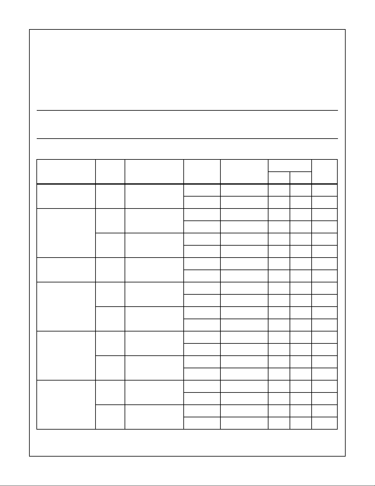
TABLE 1. DC ELECTRICAL PERFORMANCE CHARACTERISTICS
Device Tested at: V
DC PARAMETERS SYMBOL CONDITIONS
SUPPLY
= ± 15V, R
SOURCE
= 100Ω, R
= 100kΩ, V
LOAD
Thermal Resistance θ
JA
14 Lead CerDIP Package . . . . . . . . . . . . 81oC/W 26oC/W
Package Power Dissipation Limit at +75oC for TJ ≤ +175oC
14 Lead CerDIP Package . . . . . . . . . . .. . . . . . . . . . . . . . . 1.23W
Package Power Dissipation Derating Factor Above +75oC
14 Lead CerDIP Package . . . . . . . . . . . . . . . . . . . . . .12.3mW/oC
V
≤ 1/2 (V+ - V-)
INCM
RL ≥ 1kΩ
= 0V, Unless Otherwise Specified.
OUT
LIMITS
GROUP A
SUBGROUP TEMPERATURE
θ
JC
UNITSMIN MAX
Input Offset Voltage V
Input Bias Current +I
IO
VCM = 0V 1 +25oC-22mV
VCM = 0V, +RS = 1.1kΩ
B
-RS = 100Ω
-I
B
VCM = 0V, +RS = 100Ω
-RS = 1.1kΩ
Input Offset Current I
IO
VCM = 0V, +RS = 1.1kΩ
-RS = 1.1kΩ
Common Mode Range +CMR V+ = 5V
V- = -25V
-CMR V+ = 25V
V- = -5V
Large Signal Voltage
Gain
+A
-A
VOL
VOL
V
= 0V and +10V
OUT
RL = 1kΩ
V
= 0V and -10V
OUT
RL = 1kΩ
2, 3 +125oC, -55oC-6 6 mV
1 +25oC -14.5 14.5 µA
2, 3 +125oC, -55oC -20 20 µA
1 +25oC -14.5 14.5 µA
2, 3 +125oC, -55oC -20 20 µA
1 +25oC-44µA
2, 3 +125oC, -55oC-8 8 µA
1 +25oC10-V
2, 3 +125oC, -55oC10 - V
1 +25oC - -10 V
2, 3 +125oC, -55oC - -10 V
4 +25oC 20 - kV/V
5, 6 +125oC, -55oC 10 - kV/V
4 +25oC 20 - kV/V
5, 6 +125oC, -55oC 10 - kV/V
Common Mode
Rejection Ratio
+CMRR ∆VCM = 10V,
V
= -10V
OUT
V+ = 5V, V- = -25V
-CMRR ∆VCM = -10V,
V
= 10V
OUT
V+ = 25V, V- = -5V
1 +25oC75-dB
2,3 +125oC, -55oC75 - dB
1 +25oC75-dB
2, 3 +125oC, -55oC75 - dB
Spec Number 511089-883
3-54

Specifications HA-2839/883
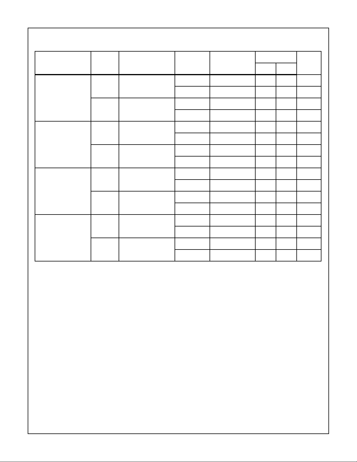
TABLE 1. DC ELECTRICAL PERFORMANCE CHARACTERISTICS (Continued)
Device Tested at: V
DC PARAMETERS SYMBOL CONDITIONS
SUPPLY
= ± 15V, R
SOURCE
= 100Ω, R
= 100kΩ, V
LOAD
= 0V, Unless Otherwise Specified.
OUT
GROUP A
SUBGROUP TEMPERATURE
LIMITS
UNITSMIN MAX
Output Voltage Swing +V
-V
Output Current +I
Quiescent Power
Supply Current
Power Supply
+PSRR ∆V
Rejection Ratio
-PSRR ∆V
-I
+I
-I
OUT
OUT
OUT
OUT
CC
CC
RL = 1kΩ 1 +25oC10-V
2, 3 +125oC, -55oC10 - V
RL = 1kΩ 1 +25oC - -10 V
2, 3 +125oC, -55oC - -10 V
V
= 10V 1 +25oC10-mA
OUT
2, 3 +125oC, -55oC10 - mA
V
= -10V 1 +25oC - -10 mA
OUT
2, 3 +125oC, -55oC - -10 mA
V
I
OUT
OUT
= 0V
= 0mA
1 +25oC - 14.6 mA
2, 3 +125oC, -55oC - 15 mA
V
I
OUT
OUT
= 0V
= 0mA
1 +25oC -14.6 - mA
2, 3 +125oC, -55oC -15 - mA
SUP
= 10V
1 +25oC75-dB
V+ = 10V, V- = -15V
V+ = 20V, V- = -15V
= 10V
SUP
2, 3 +125oC, -55oC75 - dB
1 +25oC75-dB
V+ = 15V, V- = -10V
V+ = 15V, V- = -20V
2, 3 +125oC, -55oC75 - dB
TABLE 2. AC ELECTRICAL PERFORMANCE CHARACTERISTICS
Table 2 Intentionally Left Blank. See A.C. Specifications in Table 3
Spec Number 511089-883
3-55

Device Characterized at: V
SUPPLY
Specifications HA-2839/883
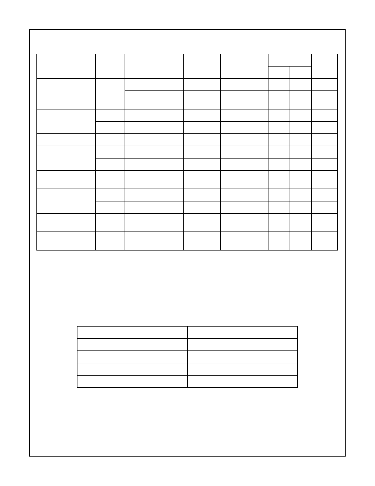
TABLE 3. ELECTRICAL PERFORMANCE CHARACTERISTICS
= ±15V, R
SOURCE
= 50Ω, R
= 1kΩ, CL≤10pF, AV = +10V/V, Unless Otherwise Specified.
LOAD
LIMITS
PARAMETERS SYMBOL CONDITIONS NOTES TEMPERATURE
Gain Bandwidth
GBWP VO = 200mV, fO = 5MHz 1 +25oC 500 - MHz
UNITSMIN MAX
Product
VO = 200mV,
1 +25oC 450 - MHz
fO = 45MHz
Slew Rate +SR VO = -5V to +5V 1, 4 +25oC 550 - V/µs
-SR VO = +5V to -5V 1, 4 +25oC 500 - V/µs
Full Power Bandwidth FPBW V
Rise and Fall Time T
Minimum Closed Loop
R
T
F
CLSG RL = 1kΩ, CL ≤ 10pF 1 -55oC to +125oC 10 - V/V
= 10V 1, 2 +25oC 8.0 - MHz
PEAK
VO = 0V to +200mV 1, 4 +25oC - 10 ns
VO = 0V to -200mV 1, 4 +25oC - 10 ns
Stable Gain
Overshoot +OS VO = 0V to +200mV 1 +25oC - 30 %
-OS VO = 0V to -200mV 1 +25oC - 30 %
Open Loop Output
R
OUT
V
= 0V 1 +25oC-60Ω
OUT
Resistance
Quiescent Power
PC V
OUT
= 0V, I
= 0mA 1, 3 -55oC to +125oC - 450 mW
OUT
Consumption
NOTES:
1. Parameters listed in Table 3 are controlled via design or process parameters and are not directly tested at final production. These parameters are lab characterized upon initial design release, or upon design changes. These parameters are guaranteed by characterization
based upon data from multiple production runs which reflect lot to lot and within lot variation.
2. Full Power Bandwidth guarantee based on Slew Rate measurement using FPBW = Slew Rate/(2πV
PEAK
).
3. Quiescent Power Consumption based upon Quiescent Supply Current test maximum. (No load on outputs.)
4. Measured between 10% and 90% points.
TABLE 4. ELECTRICAL TEST REQUIREMENTS
MIL-STD-883 TEST REQUIREMENTS SUBGROUPS (SEE TABLE 1)
Interim Electrical Parameters (Pre Burn-In) 1
Final Electrical Test Parameters 1 (Note 1), 2, 3, 4, 5, 6
Group A Test Requirements 1, 2, 3, 4, 5, 6
Groups C & D Endpoints 1
NOTE:
1. PDA applies to Subgroup 1 only.
3-56
Spec Number 511089-883
 Loading...