Intersil Corporation HA-2640-883 Datasheet

3-201
All Intersil semiconductor products are manufactured, assembled and tested under ISO9000 quality systems certification.
Intersil products are sold by description only. Intersil Corporation reserves the right to make changes in circuit design and/or specifications at any time without
notice. Accordingly, the reader is cautioned to verify that data sheets are current before placing orders. Information furnished by Intersil is believed to be accurate
and reliable. However, no responsibility is assumed by Intersil or its subsidiaries for its use; nor for any infringements of patents or other rights of third parties which
may result from its use. No license is granted by implication or otherwise under any patent or patent rights of Intersil or its subsidiaries.
For information regarding Intersil Corporation and its products, see web site http://www.intersil.com
HA-2640/883
Die Characteristics
DIE DIMENSIONS:
93 x 68 x 19 mils ± 1 mils
2360 x 1720 x 483µm ± 25.4µm
METALLIZATION:
Type: Al, 1% Cu
Thickness: 16k
Å ± 2kÅ
GLASSIVATION:
Type: Nitride (Si3N4) over Silox (SiO2, 5% Phos.)
Silox Thickness: 12k
Å ± 2kÅ
Nitride Thickness: 3.5kÅ ± 1.5kÅ
WORST CASE CURRENT DENSITY:
5.0 x 10
4
A/cm2 at 12mA
SUBSTRATE POTENTIAL (Powered Up):
Unbiased
TRANSISTOR COUNT: 76
PROCESS: HV200 Bipolar Dielectric Isolation
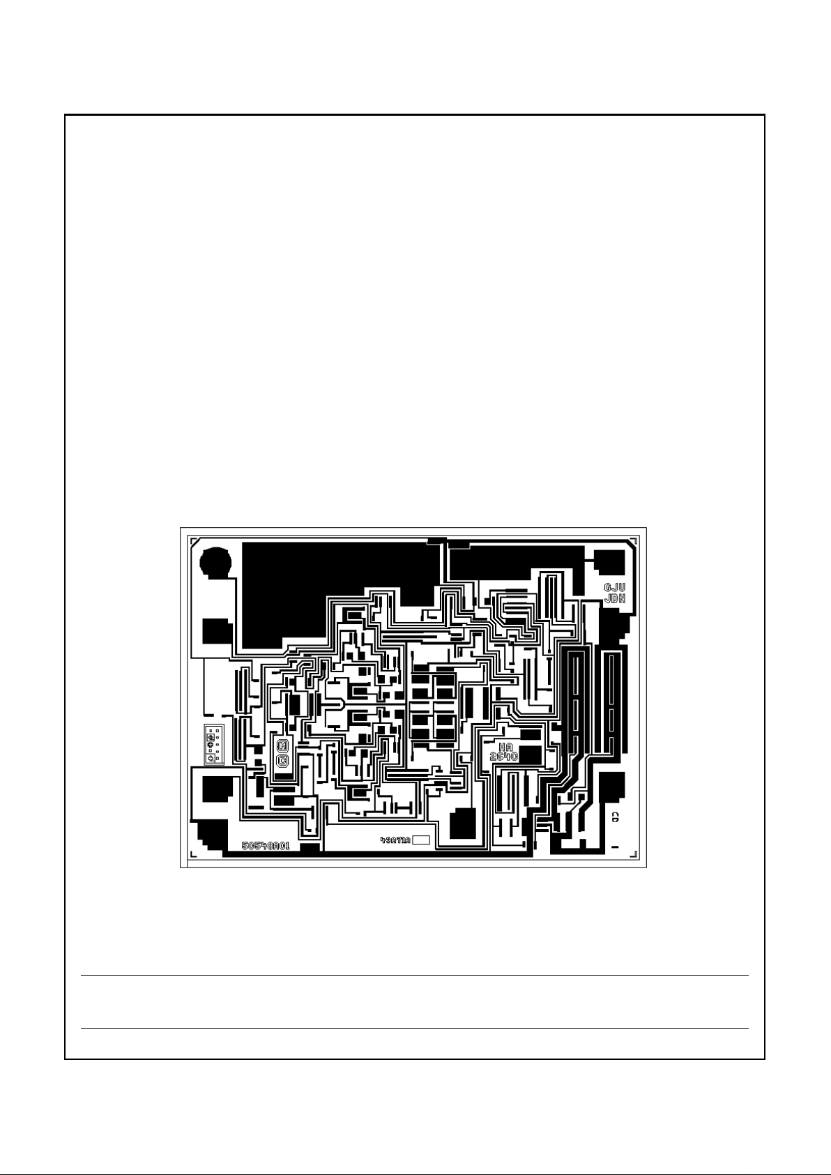
Metallization Mask Layout
HA-2640/883
COMP
V+
OUT
BALV-
+IN
-IN
BAL
Spec Number 511029-883

3-200
Spec Number
511029-883
Specifications HA-2640/883
TABLE 3. ELECTRICAL PERFORMANCE CHARACTERISTICS
Device Characterized at: V
SUPPLY
= ±40V, R
LOAD
= 5kΩ, C
LOAD
= 10pF, AV = 1V/V, Unless Otherwise Specified.
PARAMETERS SYMBOL CONDITIONS NOTES TEMPERATURE
LIMITS
UNITSMIN MAX
Differential Input Resistance R
IN
VCM = 0V 1 +25oC50-MΩ
Full Power
Bandwidth
FPBW V
PEAK
= 10V 1, 2 +25oC 45 - kHz
V
PEAK
= 35V 1, 2 +25oC 13.6 - kHz
Minimum Closed Loop
Stable Gain
CLSG RL = 5kΩ, CL = 50pF 1 -55oC to +125oC 1 - V/V
Output Short Circuit Current +I
SC
V
OUT
= 0V, RL = 10Ω 1 +25oC - 25 mA
-I
SC
V
OUT
= 0V, RL = 10Ω 1 +25oC -25 - mA
Output Resistance R
OUT
Open Loop 1 +25oC - 600 Ω
Quiescent Power
Consumption
PC V
OUT
= 0V, I
OUT
= 0mA 1, 3 -55oC to +125oC - 320 mW
NOTES:
1. Parameters listed in Table 3 are controlled via design or process parameters and are not directly tested at final production. These parameters are lab characterized upon initial design release, or upon design changes. These parameters are guaranteed by characterization
based upon data from multiple production runs which reflect lot to lot and within lot variation.
2. Full Power Bandwidth guarantee based on Slew Rate measurement using FPBW = Slew Rate/(2πV
PEAK
).
3. Power Consumption based upon Quiescent Supply Current test maximum. (No load on outputs.)
TABLE 4. ELECTRICAL TEST REQUIREMENTS
MIL-STD-883 TEST REQUIREMENTS SUBGROUPS (SEE TABLES 1 AND 2)
Interim Electrical Parameters (Pre Burn-In) 1
Final Electrical Test Parameters 1 (Note 1), 2, 3, 4, 5, 6
Group A Test Requirements 1, 2, 3, 4, 5, 6
Groups C and D Endpoints 1
NOTE:
1. PDA applies to Subgroup 1 only.
 Loading...