Intersil Corporation HA-2602-883, HA-2600-883 Datasheet

3-181
CAUTION: These devices are sensitive to electrostatic discharge; follow proper IC Handling Procedures.
1-888-INTERSIL or 321-724-7143
| Copyright © Intersil Corporation 1999
HA-2600/883
HA-2602/883
Wideband, High Impedance
Operational Amplifiers
Description
HA-2600/883 and HA-2602/883 are internally compensated
bipolar operational amplifiers that feature very high input
impedance coupled with wideband AC performance. The
high resistance of the input stage is complemented by low
offset voltage (4mV max at +25
o
C for HA-2600/883) and low
bias and offset current (10nA max at +25
o
C for HA-2600/
883) to facilitate accurate signal processing. Offset voltage
can be reduced further by means of an external nulling
potentiometer. The 4V/µs minimum slew rate at +25
o
C and
the minimum open loop gain of 100kV/V at +25
o
C enables
the HA-2600/883 to perform high gain amplification of fast,
wideband signals. These dynamic characteristics, coupled
with fast settling times, make these amplifiers ideally suited
to pulse amplification designs as well as high frequency or
video applications. The frequency response of the amplifier
can be tailored to exact design requirements by means of an
external bandwidth control capacitor. Other high performance designs such as high gain, low distortion audio
amplifiers, high-Q and wideband active filters and high
speed comparators, are excellent uses of this part.
Ordering Information
PART
NUMBER
TEMPERATURE
RANGE PACKAGE
HA2-2600/883 -55oC to +125oC 8 Pin Can
HA7-2600/883 -55oC to +125oC 8 Lead CerDIP
HA2-2602/883 -55oC to +125oC 8 Pin Can
HA7-2602/883 -55oC to +125oC 8 Lead CerDIP
Features
• This Circuit is Processed in Accordance to MIL-STD883 and is Fully Conformant Under the Provisions of
Paragraph 1.2.1.
• High Input Impedance (HA-2600/883). . . . 100MΩ (Min)
500MΩ (Typ)
• High Slew Rate. . . . . . . . . . . . . . . . . . . . . . . 4V/µs (Min)
7V/µs (Typ)
• Low Input Bias Current (HA-2600/883). . . . 10nA (Max)
1nA (Typ)
• Low Input Offset Current (HA-2600/883) . . . 4mV (Max)
• Wide Unity Gain Bandwidth . . . . . . . . . . . 12MHz (Typ)
• Output Short Circuit Protection
Applications
• Video Amplifier
• Pulse Amplifier
• High-Q Active Filters
• High Speed Comparators
• Low Distortion Oscillators
July 1994
Spec Number
511005-883
File Number 3700
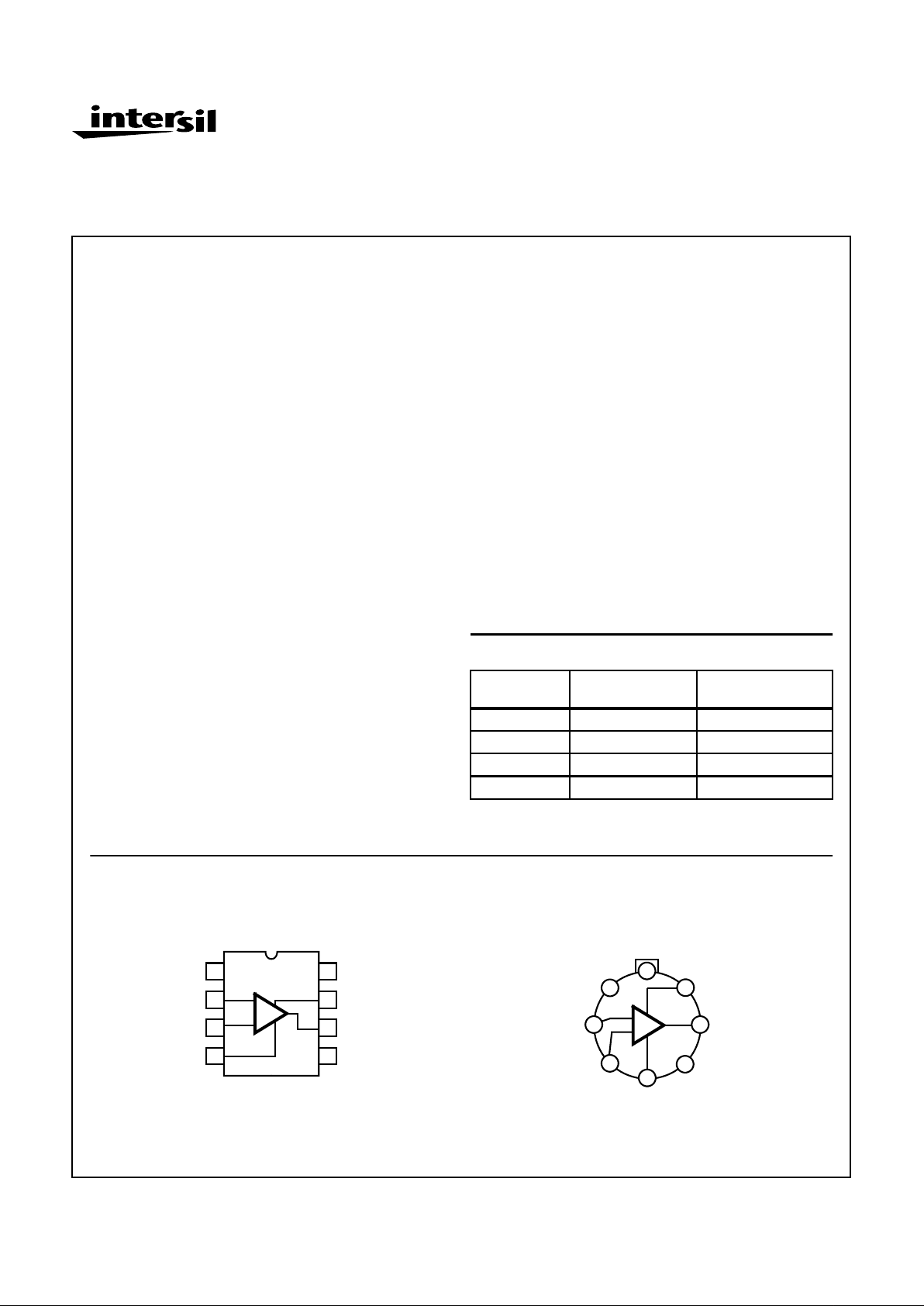
Pinouts
HA-2600/883, HA-2602/883
(CERDIP)
TOP VIEW
HA-2600/883, HA-2602/883
(METAL CAN)
TOP VIEW
1
2
3
4
8
7
6
5
COMP
V+
OUT
BAL
+
-
BAL
-IN
+IN
V-
2
4
6
1
3
7
5
8
COMP
OUT
-IN
V-
BAL
+IN
V+
BAL
+
-

3-182
Specifications HA-2600/883, HA-2602/883
Absolute Maximum Ratings Thermal Information
Voltage Between V+ and V- Terminals. . . . . . . . . . . . . . . . . . . . 40V
Differential Input Voltage . . . . . . . . . . . . . . . . . . . . . . . . . . . . . . 12V
Voltage at Either Input Terminal . . . . . . . . . . . . . . . . . . . . . . V+ to V-
Peak Output Current . . . . . . . . . . . . . . .Full Short Circuit Protection
Junction Temperature (TJ) . . . . . . . . . . . . . . . . . . . . . . . . . . +175oC
Storage Temperature Range . . . . . . . . . . . . . . . . . -65oC to +150oC
ESD Rating. . . . . . . . . . . . . . . . . . . . . . . . . . . . . . . . . . . . . . <2000V
Lead Temperature (Soldering 10s). . . . . . . . . . . . . . . . . . . . +300oC
Thermal Resistance θ
JA
θ
JC
CerDIP Package . . . . . . . . . . . . . . . . . . . 115oC/W 28oC/W
Metal Can Package. . . . . . . . . . . . . . . . . 160oC/W 75oC/W
Package Power Dissipation Limit at +75oC for TJ≤ +175oC
CerDIP Package . . . . . . . . . . . . . . . . . . . . . . . . . . . . . . . .870mW
Metal Can Package. . . . . . . . . . . . . . . . . . . . . . . . . . . . . . 625mW
Package Power Dissipation Derating Factor Above +75oC
CersDIP Package . . . . . . . . . . . . . . . . . . . . . . . . . . . . .8.7mW/oC
Metal Can Package. . . . . . . . . . . . . . . . . . . . . . . . . . . . 6.3mW/oC
CAUTION: Stresses above those listed in “Absolute Maximum Ratings” may cause permanent damage to the device. This is a stress only rating and operation
of the device at these or any other conditions above those indicated in the operational sections of this specification is not implied.
Operating Conditions
Operating Temperature Range. . . . . . . . . . . . . . . . -55oC to +125oC
Operating Supply Voltage. . . . . . . . . . . . . . . . . . . . . . . . . . . . . . . . ±15V
V
INCM
≤ 1/2 (V+ - V-)
RL≥ 2kΩ
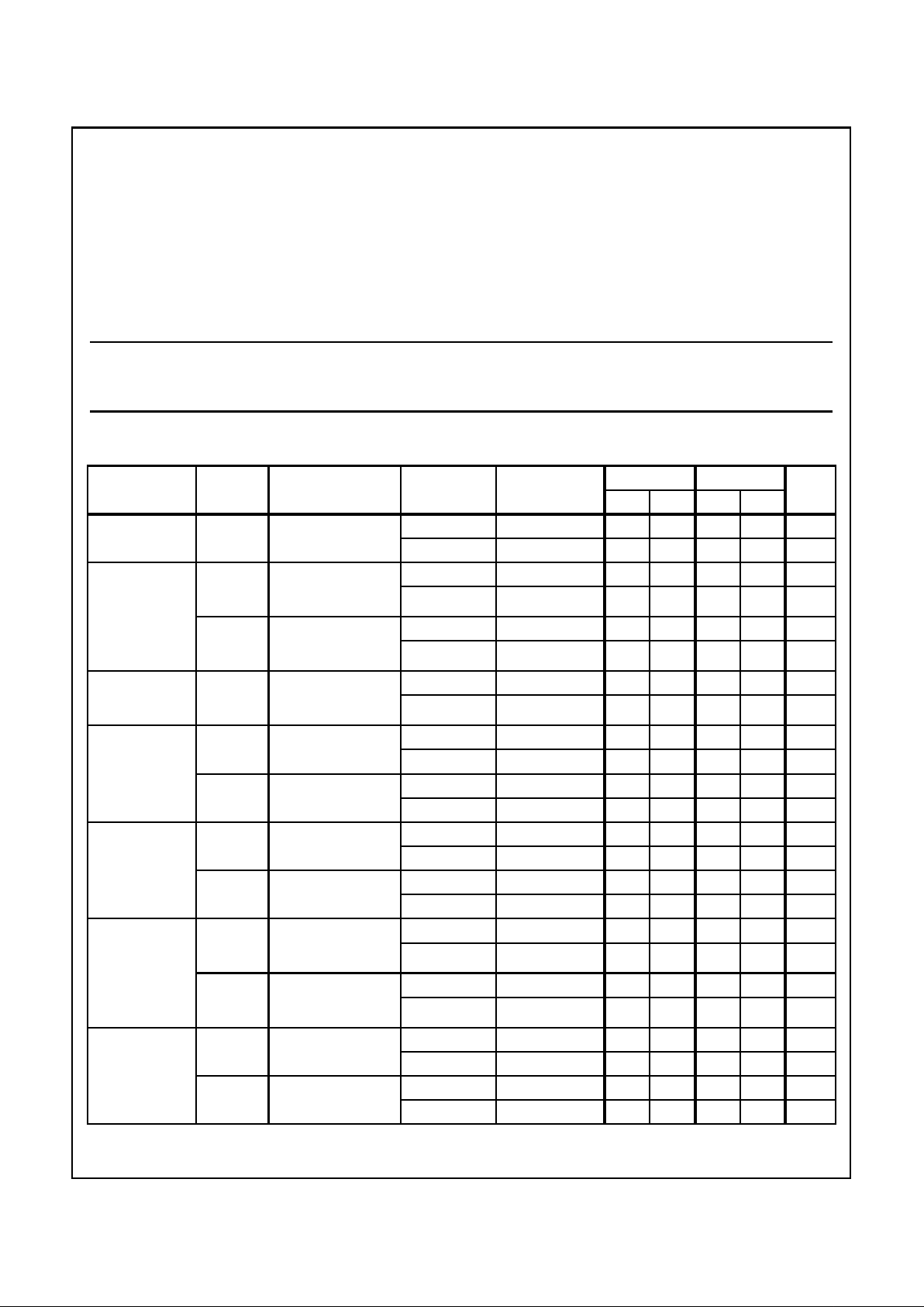
TABLE 1. DC ELECTRICAL PERFORMANCE CHARACTERISTICS
Device Tested at: V
SUPPLY
= ±15V, R
SOURCE
= 100Ω, R
LOAD
= 500kΩ, V
OUT
= 0V, Unless Otherwise Specified.
PARAMETERS SYMBOL CONDITIONS
GROUP A
SUBGROUPS TEMPERATURE
HA-2600/883 HA-2602/883
UNITSMIN MAX MIN MAX
Input Offset
Voltage
V
IO
VCM = 0V 1 +25oC -4 4 -5 5 mV
2, 3 +125oC, -55oC -6 6 -7 7 mV
Input Bias Current +I
B
VCM = 0V,
+RS = 100kΩ,
-RS = 100Ω
1 +25oC -10 10 -25 25 nA
2, 3 +125oC, -55oC -30 30 -60 60 nA
-I
B
VCM = 0V,
+RS = 100Ω,
-RS = 100kΩ
1 +25oC -10 10 -25 25 nA
2, 3 +125oC, -55oC -30 30 -60 60 nA
Input Offset
Current
I
IO
VCM = 0V,
+RS = 100kΩ,
-RS = 100kΩ
1 +25oC -10 10 -25 25 nA
2, 3 +125oC, -55oC -30 30 -60 60 nA
Common Mode
Range
+CMR V+ = +4V, V- = -26V 1 +25oC11-11-V
2, 3 +125oC, -55oC11 - 11 - V
-CMR V+ = +26V, V- = -4V 1 +25oC - -11 - -11 V
2, 3 +125oC, -55oC - -11 - -11 V
Large Signal
Voltage Gain
+A
VOL
V
OUT
= 0V and +10V,
RL = 2kΩ
4 +25oC 100 - 80 - kV/V
5, 6 +125oC, -55oC 70 - 60 - kV/V
-A
VOL
V
OUT
= 0V and -10V,
RL = 2kΩ
4 +25oC 100 - 80 - kV/V
5, 6 +125oC, -55oC 70 - 60 - kV/V
Common Mode
Rejection Ratio
+CMRR ∆VCM = +10V,
V+ = +5V, V- = -25V,
V
OUT
= -10V
1 +25oC 80 - 74 - dB
2, 3 +125oC, -55oC 80 - 74 - dB
-CMRR ∆VCM = -10V,
V+ = +25V, V- = -5V,
V
OUT
= +10V
1 +25oC 80 - 74 - dB
2, 3 +125oC, -55oC 80 - 74 - dB
Output Voltage
Swing
+V
OUT
RL = 2kΩ 4 +25oC10-10-V
5, 6 +125oC, -55oC10 - 10 - V
-V
OUT
RL = 2kΩ 4 +25oC - -10 - -10 V
5, 6 +125oC, -55oC - -10 - -10 V
Spec Number 511005-883
 Loading...