Intersil Corporation HA-2557-883 Datasheet
July 1994
HA2557/883
Wideband Four Quadrant Analog
Multiplier (Current Output)
Features
• This Circuit is Processed in Accordance to MIL-STD883 and is Fully Conformant Under the Provisions of
Paragraph 1.2.1.
• Low Multiplication Error . . . . . . . . . . . . . . . . 1.5% (Typ)
• Input Bias Currents . . . . . . . . . . . . . . . . . . . . . 8µA (Typ)
• Signal Input Feedthrough at 5MHz. . . . . . . -52dB (Typ)
• Wide Y Channel Bandwidth . . . . . . . . . . 130MHz (Typ)
• Wide X Channel Bandwidth . . . . . . . . . . . 75MHz (Typ)
• Rise Time (R
= 50Ω) . . . . . . . . . . . . . . . . . . . . 7ns (Typ)
L
• Supply Current. . . . . . . . . . . . . . . . . . . . . . . 17mA (Max)
Applications
• Military Avionics
• Missile Guidance Systems
• Medical Imaging Displays
• Video Mixers
• Sonar AGC Processors
• Radar Signal Conditioning
• Voltage Controlled Amplifier
• Vector Generator
Description
The HA-2557/883 is a monolithic, high speed, four quadrant,
analog multiplier constructed in Intersil’ Dielectrically Isolated High Frequency Process. The single-ended current
output of the HA-2557/883 has a 130MHz signal bandwidth
(R
= 50Ω). High bandwidth and low distortion make this part
L
an ideal component in video systems.
The suitability for precision video applications is demon-
strated further by low multiplication error (1.5%), low
feedthrough (-52dB), and differential inputs with low bias currents (8µA). The HA-2557/883 is also well suited for mixer
circuits as well as AGC applications for sonar, radar, and
medical imaging equipment.
The current output of the HA-2557/883 allows it to achieve
higher bandwidths than voltage output multipliers. Full scale output current is trimmed to 1.6mA. An internal 2500Ω feedback
resistor is also provided to accurately convert the current, if
desired, to a full scale output voltage of ±4V. The HA-2557/883 is
not limited to multiplication applications only; frequency doubling,
power detection, as well as many other configurations are also
possible.
Ordering Information
TEMPERATURE
PART NUMBER
HA1-2557/883 -55oC to +125oC 16 Lead CerDIP
RANGE PACKAGE
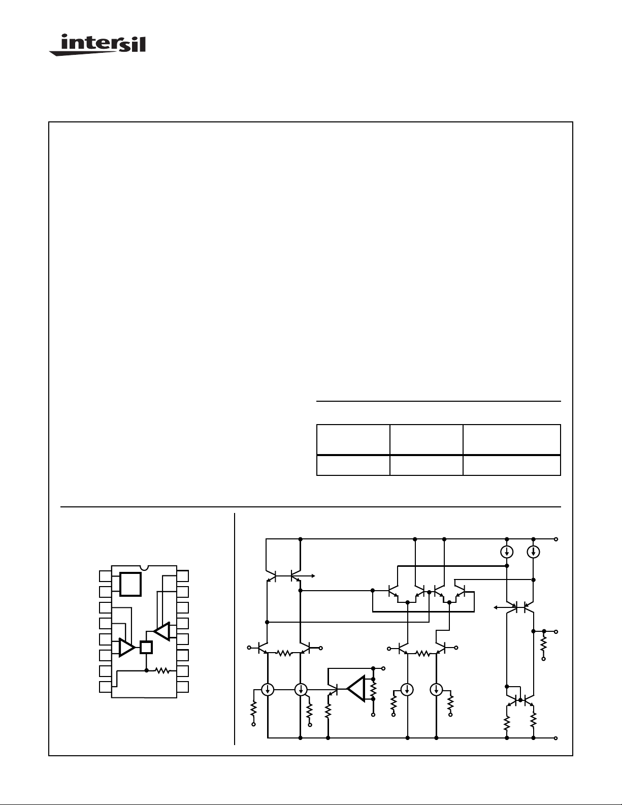
Pinout
Schematic
HA-2557/883
(CERDIP)
TOP VIEW
V
V
XIO
8-12
V
BIAS
-
X
+
-
B
GND
V
16
1
GND
V
REF
V
B
YIO
V
A
YIO
+
V
Y
-
V
Y
V-
I
OUT
CAUTION: These devices are sensitive to electrostatic discharge; follow proper IC Handling Procedures.
http://www.intersil.com or 407-727-9207
REF
2
3
4
5
Y
6
7
8
X
X
A
XIO
15
B
V
XIO
14
NC
13
+
V
X
12
-
V
X
11
V+
10
R
Z
9
NC
VX+
V
XIO
A
| Copyright © Intersil Corporation 1999
VY+
V
REF
YIO
V+
V
BIAS
I
OUT
Y
-
Y
R
Z
V
A
YIO
B
V-
Spec Number 511064-883
File Number 3638
Specifications HA2557/883
Absolute Maximum Ratings Thermal Information
Voltage Between V+ and V- . . . . . . . . . . . . . . . . . . . . . . . . . . . . 35V
Differential Input Voltage . . . . . . . . . . . . . . . . . . . . . . . . . . . . . . . 6V
Output Current . . . . . . . . . . . . . . . . . . . . . . . . . . . . . . . . . . . . . . . . .±3mA
ESD Rating. . . . . . . . . . . . . . . . . . . . . . . . . . . . . . . . . . . . . .< 2000V
Lead Temperature (Soldering 10s). . . . . . . . . . . . . . . . . . . . +300oC
Storage Temperature Range . . . . . . . . . . . . . .-65oC ≤ TA≤ +150oC
Max Junction Temperature. . . . . . . . . . . . . . . . . . . . . . . . . . +175oC
CAUTION: Stresses above those listed in “Absolute Maximum Ratings” may cause permanent damage to the device. This is a stress only rating and operation
of the device at these or any other conditions above those indicated in the operational sections of this specification is not implied.
Operating Conditions
Operating Supply Voltage (±VS) . . . . . . . . . . . . . . . . . . . . . . . . . . ±15V Operating Temperature Range . . . . . . . . . . . . -55oC ≤ TA≤ +125oC
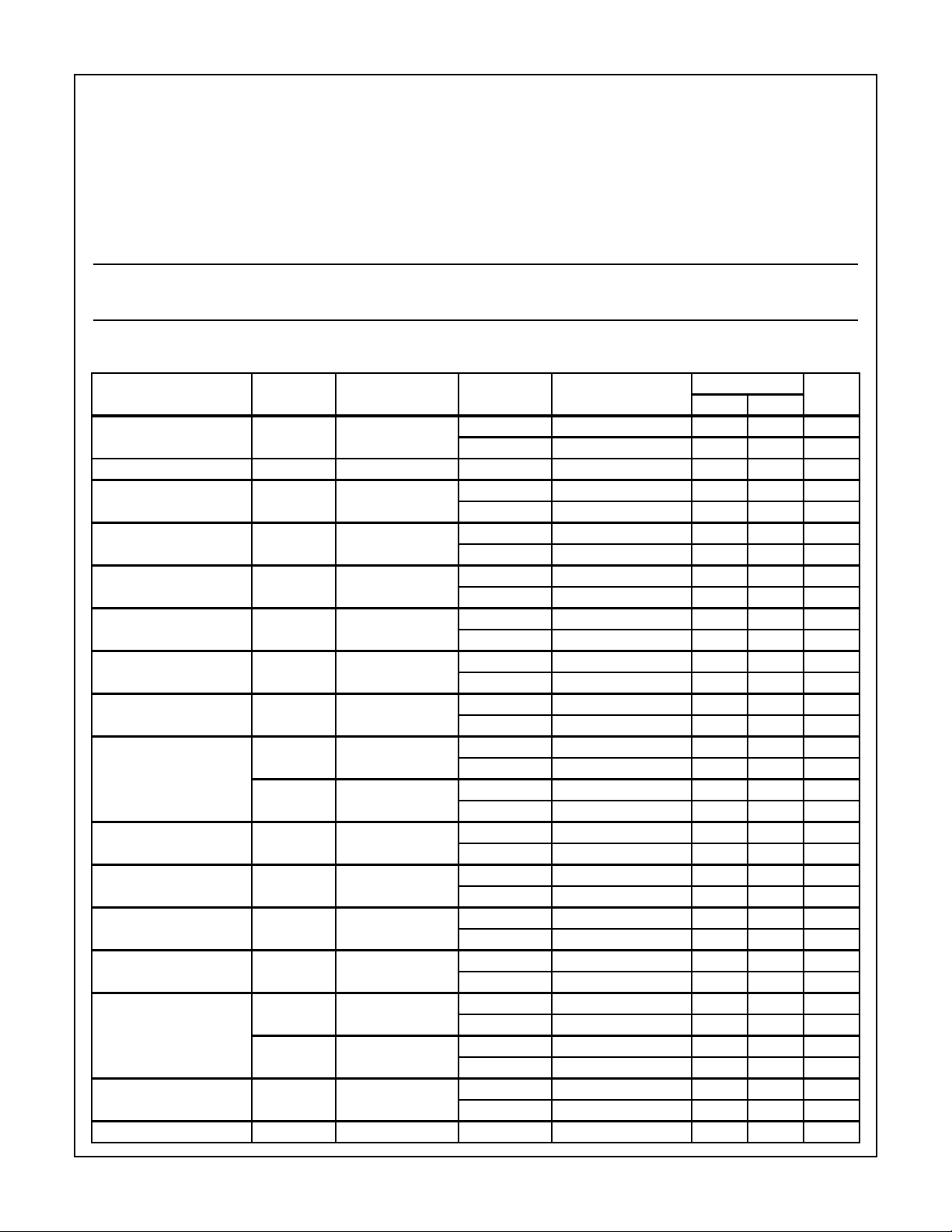
TABLE 1. DC ELECTRICAL PERFORMANCE CHARACTERISTICS
Device Tested at: V
PARAMETERS SYMBOL CONDITIONS
Multiplication Error ME VY, VX = ±4V
Linearity Error LE V
R
Accuracy RZE Nominal 2500Ω 1 +25oC-33%
Z
Offset I
I
OUT
Input Offset Voltage (V
Input Bias Current (V
Input Offset Current (V
Common Mode (V
Rejection Ratio
Power Supply (V
X
Rejection Ratio
Input Offset Voltage (V
Input Bias Current (V
Input Offset Current (V
Common Mode (V
Rejection Ratio
Power Supply (V
Y
Rejection Ratio
Supply Current I
Output Impedance Z
= ±15V, RZ (Pin 10) not connected, Unless Otherwise Specified.
SUPPLY
FS = 1.6mA
, VX = ±4V 1 +25oC -0.25 0.25 %FS
Y
VX, VY = 0V 1 +25oC -10 10 µA
VY = ±4V 1 +25oC -15 15 mV
)VX = 0V, VY = 4V 1 +25oC -15 15 µA
)VX = 0V, VY = 4V 1 +25oC-22µA
)V
X
)I
X
)I
X
)
X
CMRR(VX)VXCM = ±10V
OO
XIO
B(VX
IO(VX
VY = 4V
)
+ PSRR(VX) V+ = +12V to +17V
VY = 4V
- PSRR(V
) V- = -12V to -17V
X
VY= 4V
)V
Y
)I
Y
)I
Y
)
Y
CMRR(VY)VYCM = +9V, -10V
YIO
B(VY
IO(VY
VX = ±4V 1 +25oC -15 15 mV
)VY = 0V, VX = 4V 1 +25oC -15 15 µA
)VY = 0V, VX = 4V 1 +25oC-22µA
VX = 4V
)
+ PSRR(VY) V+ = +12V to +17V
VX = 4V
- PSRR(V
) V- = -12V to -17V
Y
VX= 4V
CC
OUT
VX, VY = 0V 1 +25oC - 17 mA
V
= ±10V 1 +25oC 1.0 - MΩ
OUT
Thermal Resistance θ
JA
θ
CerDIP Package . . . . . . . . . . . . . . . . . . . . 82oC/W 27oC/W
Maximum Package Power Dissipation at +75oC
CerDIP Package . . . . . . . . . . . . . . . . . . . . . . . . . . . . . . . . .1.22W
Package Power Dissipation Derating Factor above +75oC
CerDIP Package . . . . . . . . . . . . . . . . . . . . . . . . . . . . . . 12mW/oC
GROUP A
SUBGROUPS TEMPERATURE
LIMITS
UNITSMIN MAX
1 +25oC -3 3 %FS
2, 3 +125
2, 3 +125
2, 3 +125
2, 3 +125
2, 3 +125
2, 3 +125
o
C, -55oC -6 6 %FS
o
C, -55oC-55%
o
C, -55oC -15 15 µA
o
C, -55oC -25 25 mV
o
C, -55oC -25 25 µA
o
C, -55oC-33µA
1 +25oC65-dB
o
2, 3 +125
C, -55oC65-dB
1 +25oC65-dB
o
2, 3 +125
C, -55oC65-dB
1 +25oC45-dB
2, 3 +125
2, 3 +125
2, 3 +125
2, 3 +125
o
C, -55oC45-dB
o
C, -55oC -25 25 mV
o
C, -55oC -25 25 µA
o
C, -55oC-33µA
1 +25oC65-dB
o
2, 3 +125
C, -55oC65-dB
1 +25oC65-dB
o
2, 3 +125
C, -55oC65-dB
1 +25oC45-dB
o
2, 3 +125
2, 3 +125
C, -55oC45-dB
o
C, -55oC - 17 mA
JC
8-13
Spec Number 511064-883
HA2557/883
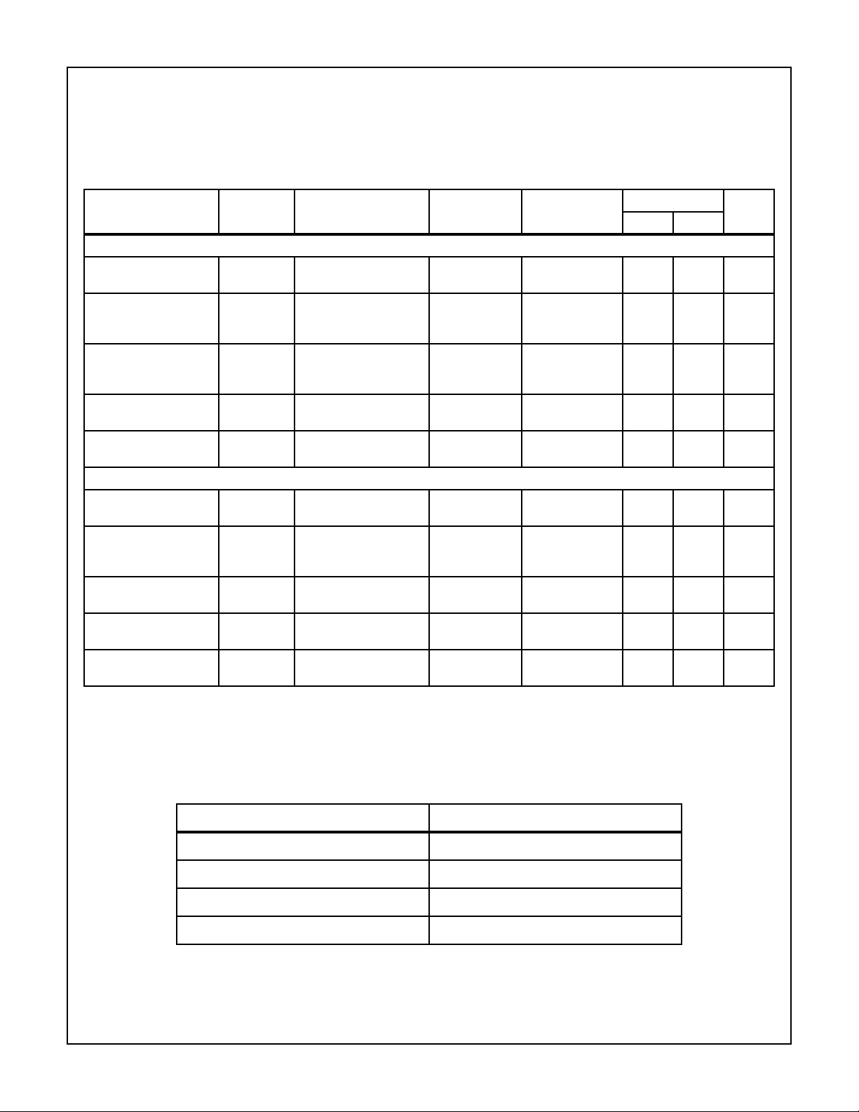
TABLE 2. AC ELECTRICAL PERFORMANCE CHARACTERISTICS
Table 2 Intentionally Left Blank. See AC Specifications in Table 3
TABLE 3. ELECTRICAL PERFORMANCE CHARACTERISTICS
Device Tested at: V
PARAMETERS SYMBOL CONDITIONS NOTES TEMPERATURE
VY, CHARACTERISTICS
Bandwidth BW(VY) -3dB, VX = 4V,
AC Feedthrough V
Rise and Fall Time TR, T
Overshoot +OS, -OS VY = -4V to +4V Step
Differential Input
Resistance
VX CHARACTERISTICS
Bandwidth BW(VX) -3dB, VY = 4V,
AC Feedthrough V
Rise and Fall Time TR, T
Overshoot +OS, -OS VX = -4V to +4V Step
Differential Input
Resistance
NOTE:
1. Parameters listed in Table 3 are controlled via design or process parameters and are not directly tested at final production. These parameters are lab characterized upon initial design release, or upon design changes. These parameters are guaranteed by characterization
based upon data from multiple production runs which reflect lot to lot and within lot variation.
2. Offset voltage applied to minimize feedthrough signal.
= ±15V, RZ (Pin 10) not connected, Unless Otherwise Specified.
SUPPLY
ISO
VY≤ 200mV
fO = 5MHz,
VY = 200mV
P-P
P-P
VX = Nulled
VY = -4V to +4V Step
F
VX = 4V,
10% to 90% pts
VX = 4V
RIN(VY)VY = ±4V, VX = 0V 1 +25oC 650 - kΩ
ISO
VX≤ 200mV
fO = 5MHz,
VX = 200mV
P-P
P-P
VY = Nulled
VX = -4V to +4V Step
F
VY = 4V, 10% to 90% pts
VY = 4V
RIN(VX)VX = ±4V, VY = 0V 1 +25oC 650 - kΩ
LIMITS
UNITSMIN MAX
1 +25oC 90 - MHz
1, 2 +25oC - -48 dB
1 +25oC - 10 ns
1 +25oC - 10 %
1 +25oC 60 - MHz
1, 2 +25oC - -50 dB
1 +25oC - 10 ns
1 +25oC - 15 %
TABLE 4. ELECTRICAL TEST REQUIREMENTS
MIL-STD-883 TEST REQUIREMENTS SUBGROUPS (SEE TABLE 1)
Interim Electrical Parameters (Pre Burn-In) -
Final Electrical Test Parameters 1 (Note 1), 2, 3
Group A Test Requirements 1, 2, 3
Groups C and D Endpoints 1
NOTE:
1. PDA applies to Subgroup 1 only.
8-14
Spec Number 511064-883
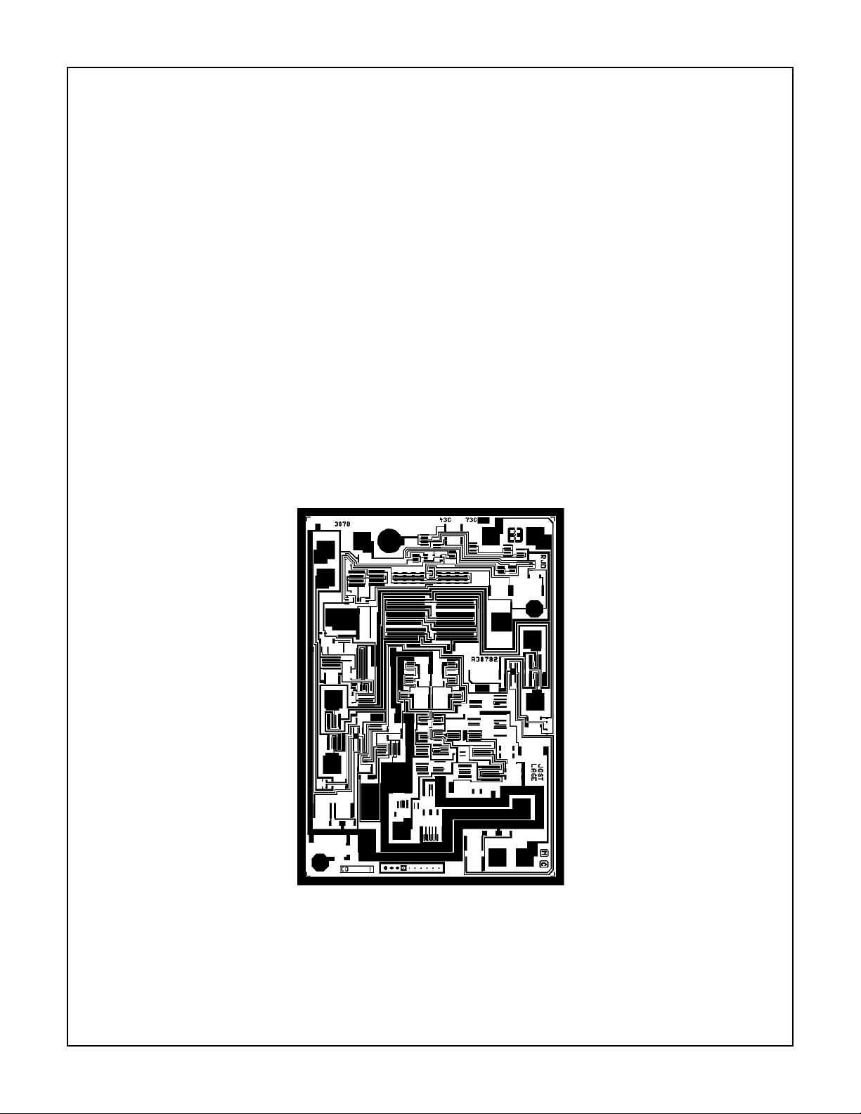
Die Characteristics
DIE DIMENSIONS:
71mils x 100mils x 19mils ± 1mils
METALLIZATION:
Type: Al, 1% Cu
Thickness: 16k
Å ± 2kÅ
GLASSIVATION:
Type: Nitride (Si
Silox Thickness: 12k
) over Silox (SiO2, 5% Phos)
3N4
Å ± 2kÅ
Nitride Thickness: 3.5kÅ ± 1.5kÅ
TRANSISTOR COUNT: 72
SUBSTRATE POTENTIAL: V-
WORST CASE CURRENT DENSITY:
0.47 x 10
5
A/cm2
Metallization Mask Layout
HA2557/883
HA-2557/883
V
YIO
V
YIO
VY+ (5)
VY- (6)
B (3)
A (4)
REF
(2) V
(1) GND
A
XIO
(16) V
B
XIO
(15) V
(13) VX+
(12) VX-
(11) V+
V- (7)
(8)
OUT
I
8-15
(10)
Z
R
Spec Number 511064-883
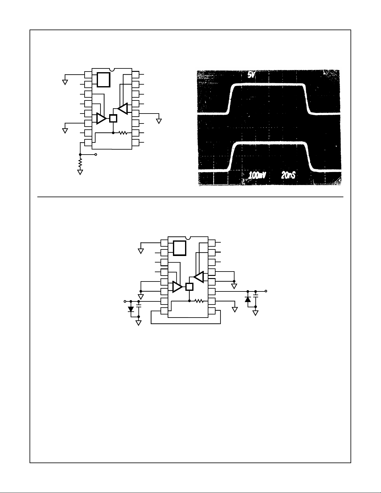
Test Circuits
NC
1
50Ω
REF
2
3
4
5
6
7
8
X
Y
V
OUT
NC
NC
NC
V
-15V
+
Y
FIGURE 1. AC AND TRANSIENT RESPONSE TEST CIRCUIT
16
15
NC
14
NC
13
+
V
X
X
12
11
+15V
10
NC
9
NC
HA2557/883
VY TRANSIENT RESPONSE
Vertical Scale: Top 5V/Div. Bottom: 100mV/Div.
Horizontal Scale: 20ns/Div.
Burn-In Circuit
- 15.5V
±0.5V
HA-2557/883 CERAMIC DIP
1
REF
2
NC
3
NC
4
NC
+
V
Y
5
Y
6
I
7
8
OUT
D1
0.01µF
D1 = D2 = 1N4002 OR EQUIVALENT (PER BOARD)
X
X
16
NC
15
NC
14
NC
V
+
X
13
12
0.01µF
+15.5 V
±0.5V
11
R
Z
10
9
D2
NC
8-16
Spec Number 511064-883
 Loading...