HA-2556
Data Sheet September 1998 File Number 2477.5
57MHz, Wideband, Four Quadrant,
Voltage Output Analog Multiplier
The HA-2556 is a monolithic, high speed, four quadrant,
analog multiplier constructed in the Intersil Dielectrically
Isolated High Frequency Process. The voltage output
simplifies many designs byeliminatingthecurrent-to-voltage
conversion stage required for current output multipliers. The
HA-2556 provides a 450V/µs slew rate and maintains
52MHz and 57MHz bandwidths for the X and Y channels
respectively, making it an ideal part for use in video systems.
The suitability for precision video applications is
demonstrated further by the Y Channel 0.1dB gain flatness
to 5.0MHz, 1.5% multiplication error,-50dB feedthrough and
differential inputs with 8µA bias current. The HA-2556 also
has low differential gain (0.1%) and phase (0.1
The HA-2556 is well suited for AGC circuits as well as mixer
applications for sonar, radar, and medical imaging
equipment. The HA-2556 is not limited to multiplication
applications only; frequency doubling, power detection, as
well as many other configurations are possible.
For MIL-STD-883 compliant product consult the
HA-2556/883 datasheet.
o
) errors.
Features
• High Speed Voltage Output . . . . . . . . . . . . . . . . . 450V/µs
• Low Multiplication Error . . . . . . . . . . . . . . . . . . . . . . .1.5%
• Input Bias Currents. . . . . . . . . . . . . . . . . . . . . . . . . . . 8µA
• 5MHz Feedthrough. . . . . . . . . . . . . . . . . . . . . . . . . .-50dB
• Wide Y Channel Bandwidth . . . . . . . . . . . . . . . . . . 57MHz
• Wide X Channel Bandwidth . . . . . . . . . . . . . . . . . . 52MHz
0.1dB Gain Flatness. . . . . . . . . . . . . . . . . . . . 5.0MHz
•V
Y
Applications
• Military Avionics
• Missile Guidance Systems
• Medical Imaging Displays
• Video Mixers
• Sonar AGC Processors
• Radar Signal Conditioning
• Voltage Controlled Amplifier
• Vector Generators
Ordering Information
TEMP.
PART NUMBER
RANGE (oC) PACKAGE
HA3-2556-9 -40 to 85 16 Ld PDIP E16.3
HA9P2556-9 -40 to 85 16 Ld SOIC M16.3
HA1-2556-9 -40 to 85 16 Ld CERDIP F16.3
PKG.
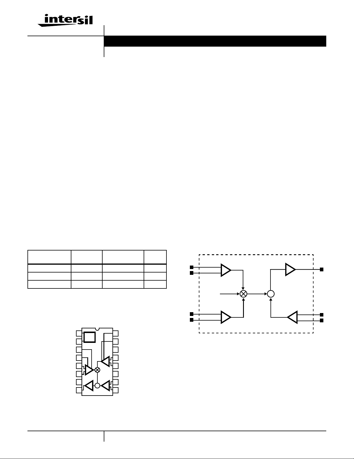
Pinout
HA-2556
(PDIP, CERDIP, SOIC)
TOP VIEW
V
16
A
XIO
V
15
B
XIO
NC
14
V
13
+
X
V
12
-
X
V+
11
10
VZ-
9
+
V
Z
V
V
GND
V
REF
YIO
YIO
V
V
V
OUT
1
REF
2
3
B
4
A
5
+
Y
Y
6
-
Y
7
V-
8
X
+
-
Σ
Z
NO.
Functional Block Diagram
VX+
+
Y
Y
1/SF
+
-
-
+
-
VX-
V
V
NOTE: The transfer equation for the HA-2556 is:
(VX+ -VX-) (VY+ -VY-) = SF (VZ+ -VZ-),
where SF = Scale Factor = 5V; VX, V
HA-2556
X
+
-
Y
VZ = Differential Inputs.
V
OUT
A
∑
Z
VZ+
+
-
V
-
Z
Y,
1
CAUTION: These devices are sensitive to electrostatic discharge; follow proper IC Handling Procedures.
1-888-INTERSIL or 321-724-7143
| Copyright © Intersil Corporation 1999

HA-2556
Absolute Maximum Ratings Thermal Information
Voltage Between V+ and V- Terminals. . . . . . . . . . . . . . . . . . . . 35V
Differential Input Voltage . . . . . . . . . . . . . . . . . . . . . . . . . . . . . . . 6V
Output Current. . . . . . . . . . . . . . . . . . . . . . . . . . . . . . . . . . . . ±60mA
Operating Conditions
Temperature Range. . . . . . . . . . . . . . . . . . . . . . . . . -40oC to 85oC
CAUTION: Stresses above those listed in “Absolute Maximum Ratings” may cause permanent damage to the device. This is a stress only rating and operation of the
device at these or any other conditions above those indicated in the operational sections of this specification is not implied.
NOTE:
1. θJA is measured with the component mounted on an evaluation PC board in free air.
Thermal Resistance (Typical, Note 1) θJA (oC/W) θJC (oC/W)
PDIP Package . . . . . . . . . . . . . . . . . . . 77 N/A
SOIC Package . . . . . . . . . . . . . . . . . . . 90 N/A
CERDIP Package. . . . . . . . . . . . . . . . . 75 20
Maximum Junction Temperature (Ceramic Package) . . . . . . . 175oC
Maximum Junction Temperature (Plastic Packages) . . . . . . 150oC
Maximum Storage Temperature Range. . . . . . . . . . -65oC to 150oC
Maximum Lead Temperature (Soldering 10s) . . . . . . . . . . . . 300oC
(SOIC - Lead Tips Only)
Electrical Specifications V
= ±15V, RF = 50Ω, RL = 1kΩ, CL = 20pF, Unless Otherwise Specified
SUPPLY
PARAMETER TEST CONDITIONS TEMP . (oC) MIN TYP MAX UNITS
MULTIPLIER PERFORMANCE
Transfer Function
V
OUT
V
–()VY+VY-–()×
X+VX-
A
-------------------------------------------------------------------- V
5
–()–=
Z+VZ-
Multiplication Error Note 2 25 - 1.5 3 %
Full - 3.0 6 %
Multiplication Error Drift Full - 0.003 - %/
o
Scale Factor 25 - 5 - V
Linearity Error V
, VY = ±3V, Full Scale = 3V 25 - 0.02 - %
X
, VY = ±4V, Full Scale = 4V 25 - 0.05 0.25 %
V
X
V
, VY = ±5V, Full Scale = 5V 25 - 0.2 0.5 %
X
AC CHARACTERISTICS
Small Signal Bandwidth (-3dB) V
Y
V
X
Full Power Bandwidth (-3dB) 10V
= 200mV
= 200mV
P-P
, VX = 5V 25 - 57 - MHz
P-P
, VY = 5V 25 - 52 - MHz
P-P
25 - 32 - MHz
Slew Rate Note 5 25 420 450 - V/µs
Rise Time Note 6 25 - 8 - ns
Overshoot Note 6 25 - 20 - %
Settling Time To 0.1%, Note 5 25 - 100 - ns
Differential Gain Notes 3, 8 25 - 0.1 0.2 %
Differential Phase Notes 3, 8 25 - 0.1 0.3 Degrees
V
0.1dB Gain Flatness 200mV
Y
0.1dB Gain Flatness 200mV
V
X
, VX = 5V, Note 8 25 4.0 5.0 - MHz
P-P
, VY = 5V, Note 8 25 2.0 4.0 - MHz
P-P
THD + N Note 4 25 - 0.03 - %
1MHz Feedthrough 200mV
5MHz Feedthrough 200mV
SIGNAL INPUT (V
, VY, V
X
Z)
, Other Ch Nulled 25 - -65 - dB
P-P
, Other Ch Nulled 25 - -50 - dB
P-P
Input Offset Voltage 25 - 3 15 mV
Full - 8 25 mV
Average Offset Voltage Drift Full - 45 - µV/oC
Input Bias Current 25 - 8 15 µA
Full - 12 20 µA
C
2

HA-2556
Electrical Specifications V
= ±15V, RF = 50Ω, RL = 1kΩ, CL = 20pF, Unless Otherwise Specified (Continued)
SUPPLY
PARAMETER TEST CONDITIONS TEMP . (oC) MIN TYP MAX UNITS
Input Offset Current 25 - 0.5 2 µA
Full - 1.0 3 µA
Differential Input Resistance 25 - 1 - MΩ
Full Scale Differential Input (V
Common Mode Range 25 - ±10 - V
V
X
Common Mode Range 25 - +9, -10 - V
V
Y
, VY, VZ)25±5- - V
X
CMRR Within Common Mode Range Full 65 78 - dB
Voltage Noise (Note 9) f = 1kHz 25 - 150 - nV/√
f = 100kHz 25 - 40 - nV/√
OUTPUT CHARACTERISTICS
Output Voltage Swing Note 10 Full ±5.0 ±6.05 - V
Output Current Full ±20 ±45 - mA
Output Resistance 25 - 0.7 1.0 Ω
POWER SUPPLY
+PSRR Note 7 Full 65 80 - dB
-PSRR Note 7 Full 45 55 - dB
Supply Current Full - 18 22 mA
NOTES:
2. Error is percent of full scale, 1% = 50mV.
3. f = 4.43MHz, V
4. f = 10kHz, VY = 1V
5. V
6. V
= 0 to ±4V.
OUT
= 0 to ±100mV.
OUT
= 300mV
Y
RMS
, 0 to 1VDC offset, VX = 5V.
P-P
, VX = 5V.
7. VS = ±12V to ±15V.
8. Guaranteed by characterization and not 100% tested.
9. VX = VY = 0V.
10. VX = 5.5V, VY = ±5.5V.
Hz
Hz
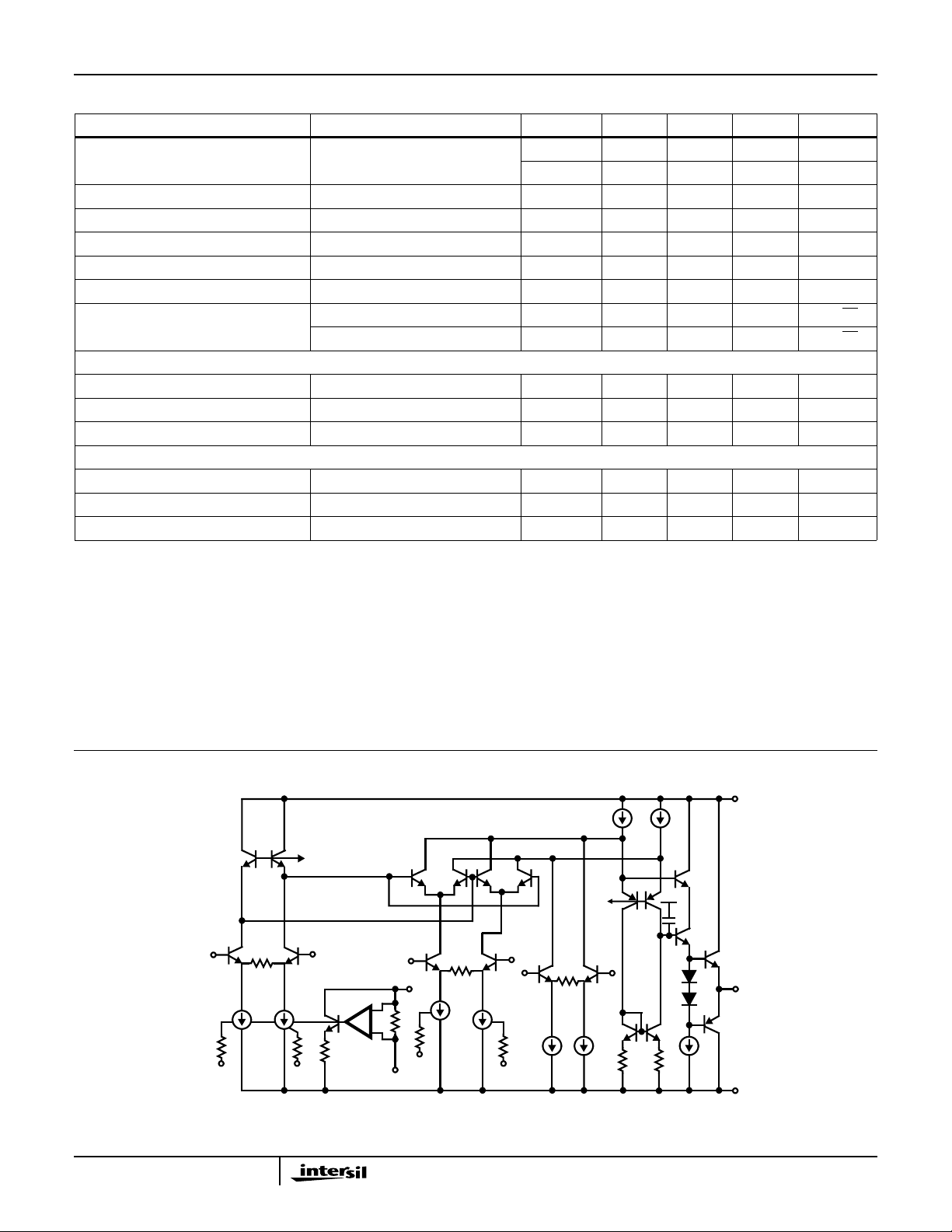
Simplified Schematic
VX+
V
AV
XIO
V+
V
BIAS
V
VX-
XIO
BIAS
+
V
Y
REF
+
-
V
A
B
YIO
GND
VY-
VZ+
V
B
YIO
VZ-
V
CC
OUT
V-
3

HA-2556
Application Information
Operation at Reduced Supply Voltages
The HA-2556 will operate over a range of supply voltages,
±5V to ±15V. Use of supply voltages below ±12V will reduce
input and output voltage ranges. See “Typical Performance
Curves” for more information.
Offset Adjustment
X and Y channel offset voltages may be nulled by using a
20K potentiometer between the V
YIO
or V
adjust pin A
XIO
and B and connecting the wiper to V-.Reducing the channel
offset voltage will reduce AC feedthrough and improve the
multiplication error. Output offset voltage can also be nulled
by connecting V
- to the wiper of a potentiometer which is
Z
tied between V+ and V-.
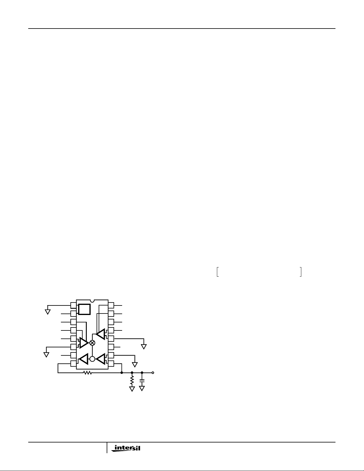
Capacitive Drive Capability
When driving capacitive loads >20pF a 50Ω resistor should
be connected between V
output (see Figure 1). This will prevent the multiplier from
going unstable and reduce gain peaking at high frequencies.
The 50Ω resistor will dampen the resonance formed with the
capacitive load and the inductance of the output at pin 8.
Gain accuracy will be maintained because the resistor is
inside the feedback loop.
and VZ+, using VZ+ as the
OUT
Theory of Operation
The HA-2556 creates an output voltage that is the product
of the X and Y input voltages divided by a constant scale
factor of 5V. The resulting output has the correct polarity in
each of the four quadrants defined by the combinations of
positive and negative X and Y inputs. The Z stage provides
the means for negative feedback (in the multiplier
configuration) and an input for summation into the output.
This results in the following equation, where X, Y and Z are
high impedance differential inputs
1
REF
NC
NC
NC
V
-15V
2
3
4
5
+
Y
FIGURE 1. DRIVING CAPACITIVE LOAD
+
-
6
7
8
Σ
50Ω
.
16
NC
15
NC
14
NC
13
+
-
+
-
-
+
VX+
12
11
+15 V
VZ-
10
9
1kΩ
+
V
Z
V
OUT
20pF
To accomplish this the differential input voltages are first
converted into differential currents by the X and Y input
transconductance stages. The currents are then scaled by a
constant reference and combined in the multiplier core. The
multiplier core is a basic Gilbert Cell that produces a
differential output current proportional to the product of X and
Y input signal currents. This current becomes the output for
the HA-2557.
The HA-2556 takes the output current of the core and feeds it
to a transimpedance amplifier, that con verts the current to a
voltage. In the multiplier configuration, negative feedback is
provided with the Z transconductance amplifier by connecting
V
to the Z input. The Z stage converts V
OUT
to a current
OUT
which is subtracted from the multiplier core before being
applied to the high gain transimpedanceamp.The Z stage, by
virtue of it’s similarity to the X and Y stages, also cancels
second order errors introduced by the dependence of V
BE
on
collector current in the X and Y stages.
The purpose of the reference circuit is to provide a stable
current, used in setting the scale factor to 5V. This is
achieved with a bandgap reference circuit to produce a
temperature stable voltage of 1.2V which is forced across a
NiCr resistor. Slight adjustments to scale factor may be
possible by overriding the inter nal reference with the V
REF
pin. The scale factor is used to maintain the output of the
multiplier within the normal operating range of ±5V when
full scale inputs are applied.
The Balance Concept
The open loop transfer equation for the HA-2556 is:
VX+-V
()xVY+V–
V
OUT
------------------------------------------------------------------ -
= A
where;
A = Output Amplifier Open Loop Gain
V
X, VY,VZ
= Differential Input Voltages
5V = Fixed Scaled Factor
An understanding of the transfer function can be gained by
assuming that the open loop gain, A, of the output amplifier
is infinite. With this assumption, any value of V
generated with an infinitesimally small value for the terms
within the brackets. Therefore we can write the equation:
()xVY+-V
V
X+-VX-
---------------------------------------------------------------- -
0 =
5V
which simplifies to:
V
()xVY+-V
X+-VX-
()= 5V VZ+-V
()
X-
5V
()
Y-
Y-
Y-
()
-V
Z+-VZ-
()
-VZ+-V
()
Z-
OUT
Z-
can be
V
OUT
= Z
=
X x Y
------------- -
5
This form of the transfer equation provides a useful tool to
analyze multiplier application circuits and will be called the
Balance Concept.
4

HA-2556
Typical Applications
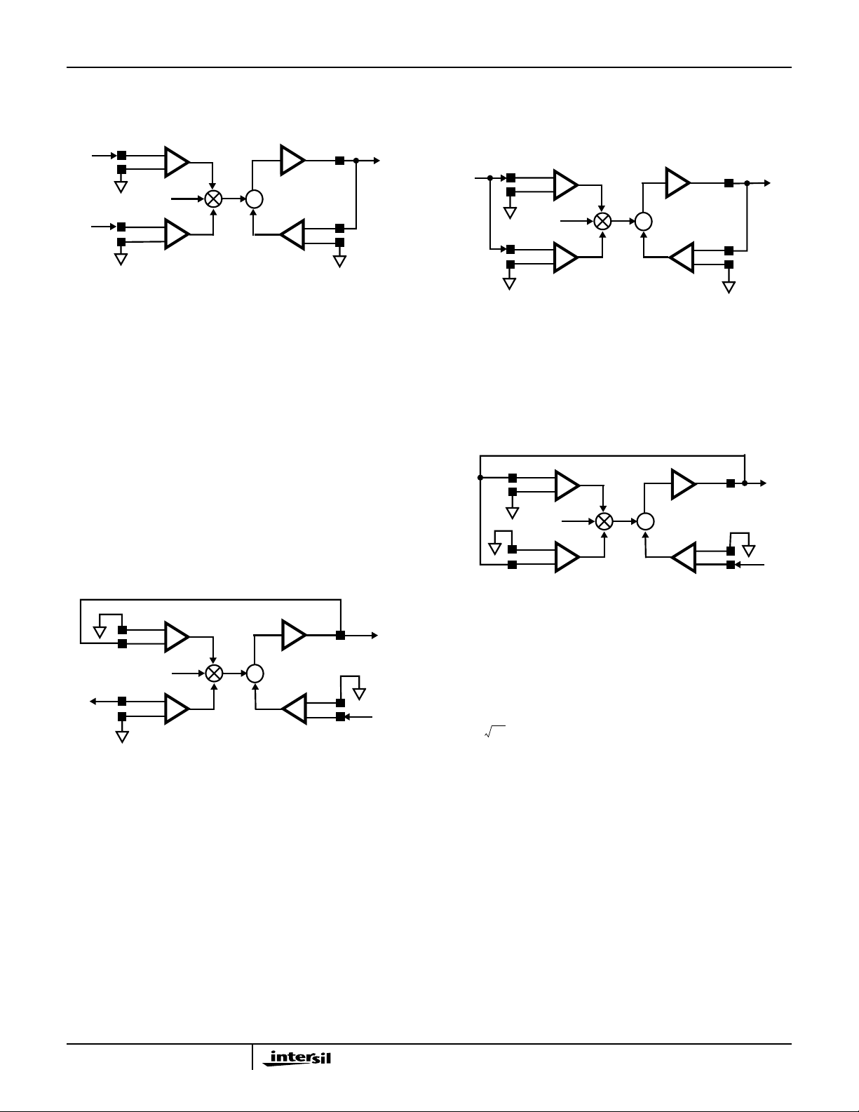
Let’s first examine the Balance Concept as it applies to the
standard multiplier configuration (Figure 2).
A
B
Signals A and B are input to the multiplier and the signal W
is the result. By substituting the signal values into the
Balance equation you get:
(A) x (B) = 5(W)
And solving for W:
W =
Notice that the output (W) enters the equation in the
feedbacktotheZstage.TheBalanceEquationdoes not test
for stability, so remember that you must provide negative
feedback.Inthemultiplierconfiguration, the feedback path is
connected to V
that takes place at the summing node just prior to the output
amplifier. Feedback is not restricted to the Z stage, other
feedback paths are possible as in the Divider Configuration
shown in Figure 3.
A x B
------------- -
5
VX+
VX-
V
Y
V
Y
1/5V
+
-
HA-2556
+
-
X
+
∑
-
Y
+
-
Z
V
OUT
A
+
V
Z
+
-
V
-
Z
FIGURE 2. MULTIPLIER
+ input, not VZ-. This is due to the inversion
Z
W
Here the Balance equation will appear as:
(A) x (A) 5(W)=
A
VX+
V
X
VY+
V
Y
-
1/5V
-
HA-2556
+
-
X
+
∑
-
Y
+
-
Z
V
OUT
A
VZ+
+
-
-
V
Z
FIGURE 4. SQUARE
Which simplifies to:
2
A
W
------ -=
5
The last basic configuration is the Square Root as shown in
Figure 5. Here feedback is provided to both X and Y inputs.
VX+
V
VY+
V
+
-
-
X
1/5V
+
-
-
Y
HA-2556
X
Y
V
OUT
A
+
∑
-
Z
+
V
Z
+
-
-
V
Z
W
A
W
VX+
+
-
V
X
1/5V
+
V
B
Y
+
-
V
Y
HA-2556
-
X
+
∑
-
Y
Z
-
V
OUT
A
+
V
Z
+
-
-
V
Z
W
A
FIGURE 3. DIVIDER
Inserting the signal values A, B and W into the Balance
Equation for the divider configuration yields:
-W()B() 5V x -A()=
Solving for W yields:
5A
------ -
W =
B
Notice that, in the dividerconfiguration,signalBmustremain
≥0 (positive) for the feedback to be negative. If signal B is
negative,thenitwillbemultipliedbytheV
input to produce
X-
positive feedback and the output will swing into the rail.
Signals may be applied to more than one input at a time as
in the Squaring configuration in Figure 4:
FIGURE 5. SQUARE ROOT (FOR A > 0)
The Balance equation takes the form:
W() W–()× 5A–()=
Which equates to:
W5A=
The four basic configurations (Multiply, Divide, Square and
Square Root) as well as variations of these basic circuits
have many uses.
Frequency Doubler
For example, if ACos(ωτ) is substituted for signal A in the
Square function, then it becomes a Frequency Doubler and
the equation takes the form:
ACos ωτ()()ACos ωτ()()× 5W()=
And using some trigonometric identities gives the result:
2
A
------ -
W
10
1Cos2ωτ()+()=
5
 Loading...