Intersil Corporation HA-2546-883 Datasheet
July 1994
HA2546/883
Wideband Two Quadrant Analog
Multiplier (Voltage Output)
Features
• This Circuit is Processed in Accordance to MIL-STD883 and is Fully Conformant Under the Provisions of
Paragraph 1.2.1.
• High Speed Voltage Output. . . . . . . . . . . 300V/µs (Min)
• Low Multiplication Error . . . . . . . . . . . . . . . .3.0% (Max)
1.6% (Typ)
• Input Bias Currents . . . . . . . . . . . . . . . . . . . . 5µA (Max)
1.2µA (Typ)
• Signal Input Feedthrough . . . . . . . . . . . . . .-52dB (Typ)
• Wide Signal Bandwidth. . . . . . . . . . . . . . . 30MHz (Typ)
• Wide Control Bandwidth. . . . . . . . . . . . . . 17MHz (Typ)
• Gain Flatness to 5MHz. . . . . . . . . . . . . . . .0.10dB (Typ)
Applications
• Military Avionics
• Missile Guidance Systems
• Medical Imaging Displays
• Video Mixers
• Sonar AGC Processors
• Radar Signal Conditioning
Description
The HA-2546/883 is a monolithic, high speed, two quadrant,
analog multiplier constructed in the Intersil Dielectrically Isolated High Frequency Process. The HA-2546/883 has a voltage output with a 30MHz signal bandwidth, 300V/µs slew
rate and a 17MHz control input bandwidth. High bandwidth
and slew rate make this part an ideal component for use in
video systems. The suitability for precision video applications is demonstrated further by the 0.1dB gain flatness at
5MHz, 1.6% multiplication error, -52dB feedthrough and differential inputs with 1.2µA bias currents. The HA-2546/883
also has low differential gain (0.1% typ.) and phase (0.1
typ.) errors.
The HA-2546/883 is well suited for AGC circuits as well as
mixer applications for sonar, radar, and medical imaging
equipment. The voltage output of the HA-2546/883 simplifies
many designs by eliminating the current-to-voltage conversion stage required for current output multipliers.
Ordering Information
TEMPERATURE
PART NUMBER
HA1-2546/883 -55oC to +125oC 16 Lead CerDIP
HA4-2546/883 -55oC to +125oC 20 Lead Ceramic LCC
RANGE PACKAGE
o
• Voltage Controlled Amplifier
• Vector Generator
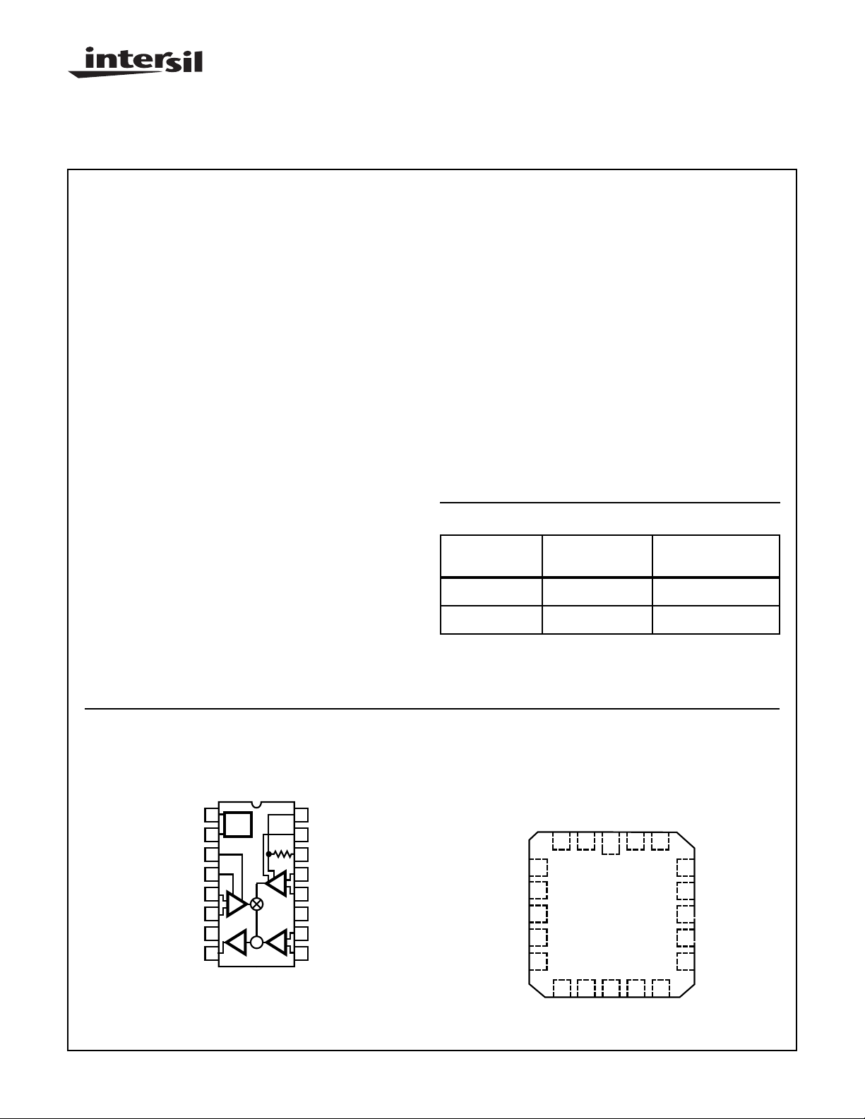
Pinouts
HA-2546/883
(CERDIP)
TOP VIEW
GA A
1
GND
V
REF
V
YIO
V
YIO
V
V
V
OUT
CAUTION: These devices are sensitive to electrostatic discharge; follow proper IC Handling Procedures.
http://www.intersil.com or 407-727-9207
REF
2
3
B
4
A
+
5
+
Y
Y
6
-
Y
-
7
V-
8
| Copyright © Intersil Corporation 1999
16
GA C
15
GA B
14
+
V
13
+
X
+
-
Σ
X
V
12
-
X
-
V+
11
-
10
VZ-
Z
9
+
V
Z
+
V
YIO
V
YIO
NC
V
Y
V
8-3
HA-2546/883
(CLCC)
TOP VIEW
REF
V
GNDNCGA A
3212019
B
4
A
5
6
+
7
-
8
Y
10 11 12 139
V-
OUT
V
NC
GA C
GA B
18
+
V
17
X
NC
16
-
V
15
X
V+
14
-
+
Z
Z
V
V
Spec Number 511050-883
File Number 2444.1

Specifications HA2546/883
Absolute Maximum Ratings Thermal Information
Voltage Between V+ and V- . . . . . . . . . . . . . . . . . . . . . . . . . . . . 35V
Differential Input Voltage . . . . . . . . . . . . . . . . . . . . . . . . . . . . . . . 6V
Output Current . . . . . . . . . . . . . . . . . . . . . . . . . . . . . . . . . . . . .60mA
Junction Temperature. . . . . . . . . . . . . . . . . . . . . . . . . . . . . . +175oC
Storage Temperature Range . . . . . . . . . . . . . .-65oC ≤ TA≤ +150oC
ESD Rating. . . . . . . . . . . . . . . . . . . . . . . . . . . . . . . . . . . . . . <2000V
Lead Temperature (Soldering 10s). . . . . . . . . . . . . . . . . . . . +300oC
CAUTION: Stresses above those listed in “Absolute Maximum Ratings” may cause permanent damage to the device. This is a stress only rating and operation
of the device at these or any other conditions above those indicated in the operational sections of this specification is not implied.
Operating Conditions
Operating Temperature Range. . . . . . . . . . . . . . . . -55oC to +125oC Operating Supply Voltage. . . . . . . . . . . . . . . . . . . . . . . . . . ±8V to ±15V
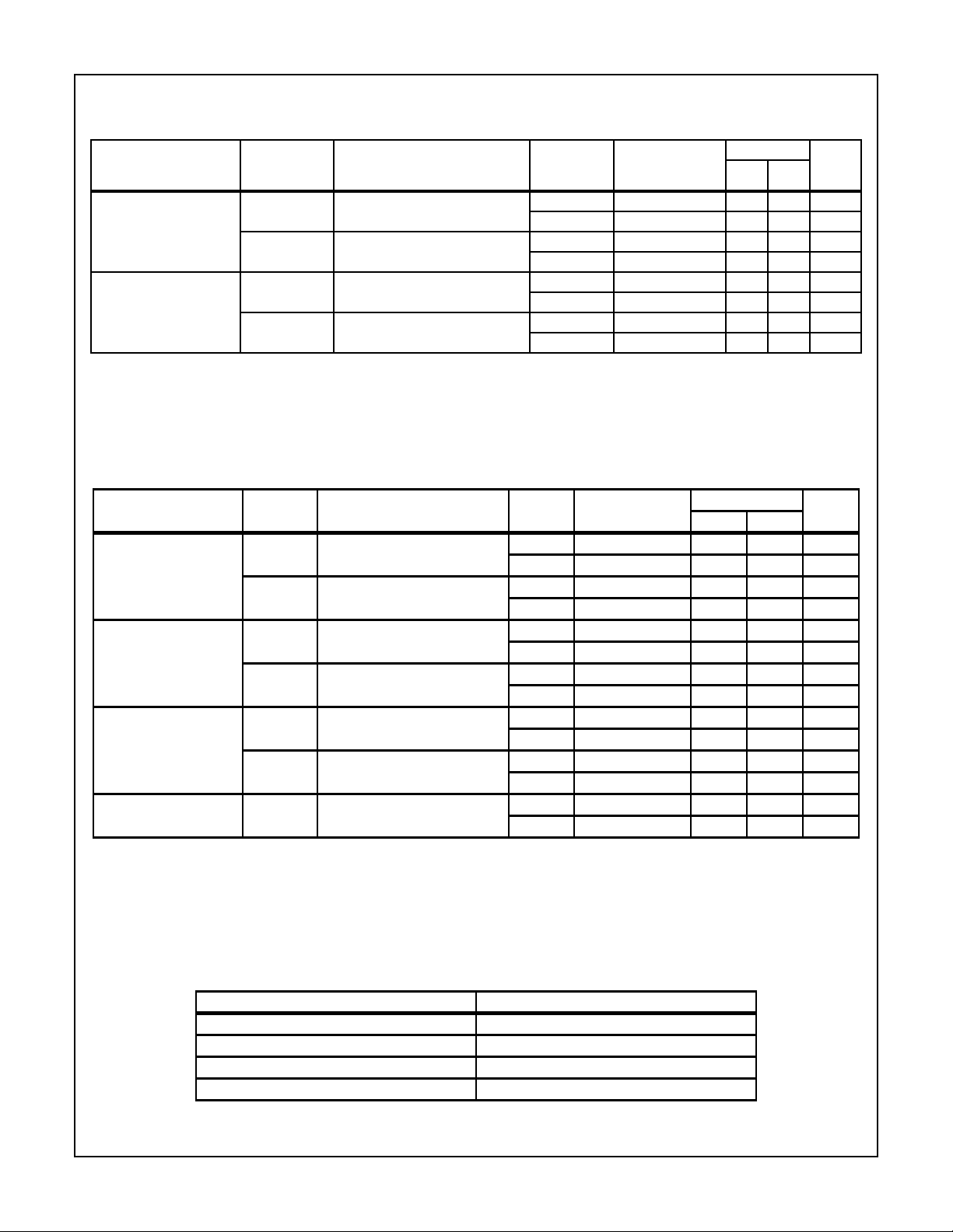
TABLE 1. DC ELECTRICAL PERFORMANCE CHARACTERISTICS
Device Tested at: V
PARAMETERS SYMBOL CONDITIONS
Multiplication Error ME VY = ±5V 1 +25oC -3 3 %FS
Scale Factor Error SF 1 +25oC-55%
Common Mode Range +CMR 1 +25oC5-V
Input Offset Voltage (VY)VIO(VY)VCM = 0V 1 +25oC -10 10 mV
Input Bias Current (VY)I
Input Offset Current (VY)IIO(VY)VCM = 0V 1 +25oC-22µA
Common Mode (VY)
Rejection Ratio
Input Offset Voltage (VX)VIO(VX)VCM = 0V 1 +25oC-22mV
Input Bias Current (VX)I
Input Offset Current (VX)IIO(VX)VCM = 0V 1 +25oC-22µA
Input Offset Voltage (VZ)VIO(VZ)VX = 0V, VY = 0V 1 +25oC -15 15 mV
Output Voltage Swing +V
Output Current +I
SUPPLY
= ±15V, R
LOAD
= 1kΩ, C
= 50pF, Unless Otherwise Specified.
LOAD
-CMR 1 +25oC - -5 V
)VCM = 0V 1 +25oC -15 15 µA
B(VY
+CMRR(VY)VY = 0 to +5V, VX = +2V 1 +25oC60-dB
-CMRR(VY)VY = 0 to -5V, VX = +2V 1 +25oC60-dB
)VCM = 0V 1 +25oC-22µA
B(VX
OUT
-V
OUT
OUT
-I
OUT
VY = +5V, VX = +2.5V 1 +25oC5-V
VY = -5V, VX = +2.5V 1 +25oC - -5 V
VY = +5V, VX = +2.5V 1 +25oC20-mA
VY = -5V, VX = +2.5V 1 +25oC - -20 mA
Thermal Resistance θ
JA
CerDIP Package . . . . . . . . . . . . . . . . . . . . . 80oC/W 25oC/W
Ceramic LCC. . . . . . . . . . . . . . . . . . . . . . . . 61oC/W 12oC/W
Maximum Package Power Dissipation
CerDIP Package at +75oC. . . . . . . . . . . . . . . . . . . . . . . . . . 1.25W
Ceramic LCC Package at +75oC. . . . . . . . . . . . . . . . . . . . . 1.64W
Package Power Dissipation Derating Factor above +75oC
CerDIP Package . . . . . . . . . . . . . . . . . . . . . . . . . . . . . . 12mW/oC
Ceramic LCC Package . . . . . . . . . . . . . . . . . . . . . . . . . 16mW/oC
GROUP A
LIMITS
SUBGROU
PS TEMPERATURE
UNITSMIN MAX
2, 3 +125oC, -55oC -5 5 %FS
2, 3 +125oC, -55oC-55 %
2, 3 +125oC, -55oC5 - V
2, 3 +125oC, -55oC - -5 V
2, 3 +125oC, -55oC -15 15 mV
2, 3 +125oC, -55oC -20 20 µA
2, 3 +125oC, -55oC-33 µA
2, 3 +125oC, -55oC60 - dB
2, 3 +125oC, -55oC60 - dB
2, 3 +125oC, -55oC -15 15 mV
2, 3 +125oC, -55oC-55 µA
2, 3 +125oC, -55oC-33 µA
2, 3 +125oC, -55oC -15 15 mV
2, 3 +125oC, -55oC5 - V
2, 3 +125oC, -55oC - -5 V
2, 3 +125oC, -55oC20 - mA
2, 3 +125oC, -55oC - -20 mA
θ
JC
8-4
Spec Number 511050-883
Specifications HA2546/883
(Continued)
LIMITS
Device Tested at: V
TABLE 1. DC ELECTRICAL PERFORMANCE CHARACTERISTICS
SUPPLY
= ±15V, R
LOAD
= 1kΩ, C
= 50pF, Unless Otherwise Specified.
LOAD
GROUP A
SUBGROU
PARAMETERS SYMBOL CONDITIONS
Power Supply Rejection
Ratio
+PSRR ∆ VS = 3V, V+ = +15V, V- = -15V,
V+ = +12V, V- = -15V
-PSRR ∆ VS = 3V, V+ = +15V, V- = -15V,
V+ = +15V, V- = -12V
Quiescent Power Supply
+I
CC
VX = VY = 0V, I
Current
-I
CC
VX = VY = 0V, I
= 0mA 1 +25oC29-mA
OUT
= 0mA 1 +25oC - -29 mA
OUT
PS TEMPERATURE
UNITSMIN MAX
1 +25oC58-dB
2, 3 +125oC, -55oC58 - dB
1 +25oC58-dB
2, 3 +125oC, -55oC58 - dB
2, 3 +125oC, -55oC29 - mA
2, 3 +125oC, -55oC - -29 mA
TABLE 2. AC ELECTRICAL PERFORMANCE CHARACTERISTICS
Table 2 Intentionally Left Blank. See AC Specifications in Table 3.
TABLE 3. ELECTRICAL PERFORMANCE CHARACTERISTICS
Device Tested at: V
SUPPLY
= ±15V, R
LOAD
= 1kΩ, C
= 50pF, Unless Otherwise Specified.
LOAD
LIMITS
PARAMETER SYMBOL CONDITIONS NOTES TEMPERATURE
Slew Rate +SR V
= -5V to +5V, VX = 2V
OUT
DC
1 +25oC 300 - V/µs
UNITSMIN MAX
1 +125oC, -55oC 300 - V/µs
-SR V
= +5V to -5V, VX = 2V
OUT
DC
1 +25oC 300 - V/µs
1 +125oC, -55oC 300 - V/µs
Rise and Fall Time TR V
TF V
Overshoot +OS V
-OS V
Full Power Bandwidth FPBW V
= -100mV to +100mV
OUT
VX = 2V
DC
= +100mV to -100mV
OUT
VX = 2V
DC
= -100mV to +100mV
OUT
VX = 2V
DC
= +100mV to -100mV
OUT
VX = 2V
DC
= 5V, VX = 2V
PEAK
DC
1, 3 +25oC - 15 ns
1, 3 +125oC, -55oC - 17 ns
1, 3 +25oC - 15 ns
1, 3 +125oC, -55oC - 17 ns
1 +25oC - 30 %
1 +125oC, -55oC - 30 %
1 +25oC - 30 %
1 +125oC, -55oC - 30 %
1, 2 +25oC 9.5 - MHz
1, 2 +125oC, -55oC 9.5 - MHz
NOTES:
1. Parameters listed in Table 3 are controlled via design or process parameters and are not directly tested at final production. These parameters are lab characterized upon initial design release, or upon design changes. These parameters are guaranteed by characterization
based upon data from multiple production runs which reflect lot to lot and within lot variation.
2. Full Power Bandwidth guarantee based on Slew Rate measurement using FPBW = Slew Rate/(2πV
PEAK
).
3. Measured between 10% and 90% points.
TABLE 4. ELECTRICAL TEST REQUIREMENTS
MIL-STD-883 TEST REQUIREMENTS SUBGROUPS (SEE TABLE 1)
Interim Electrical Parameters (Pre Burn-in) 1
Final Electrical Test Parameters 1(Note 1), 2, 3
Group A Test Requirements 1, 2, 3
Groups C and D Endpoints 1
NOTE:
1. PDA applies to Subgroup 1 only.
8-5
Spec Number 511050-883
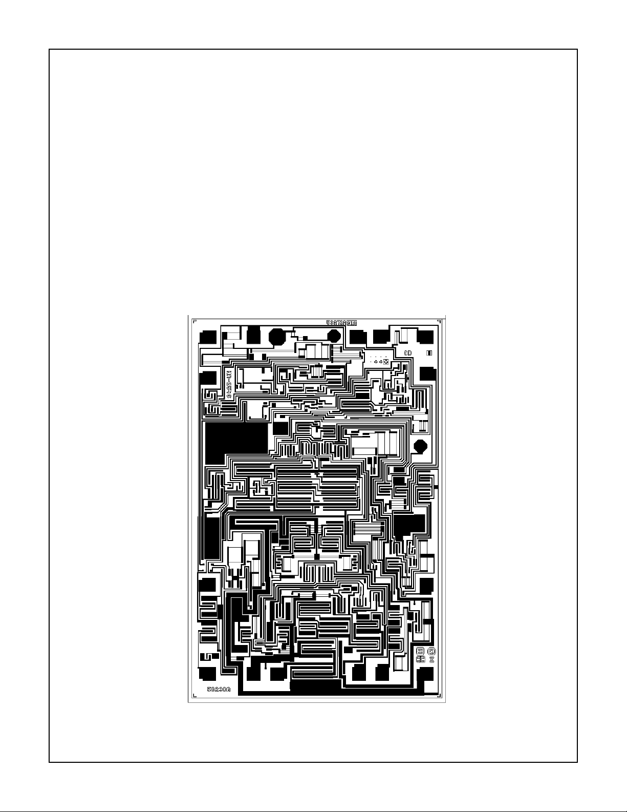
Die Characteristics
DIE DIMENSIONS:
79.9mils x 119.7mils x 19mils± 1mils
METALLIZATION:
Type: Al, 1%Cu
Thickness: 16k
Å ± 2kÅ
GLASSIVATION:
Type: Nitride (Si
Silox Thickness: 12k
) over Silox (SiO2, 5% Phos)
3N4
Å ± 1.5kÅ
Nitride Thickness: 3.5kÅ ± 1.5kÅ
WORST CASE CURRENT DENSITY:
0.72 x 10
5
A/cm
2
TRANSISTOR COUNT: 87
Metallization Mask Layout
V
REF
(2) (1)
HA2546/883
HA-2546/883
GND
GA A GA C
(15)(16)
V
B (3)
YIO
V
A (4)
YIO
+ (5)
V
Y
(14) GA B
(13) V
+
X
(12) VX-
VY- (6)
(7) (8) (9) (10)
V-
V
OUT
VZ+VZ-
8-6
(11) V+
Spec Number 511050-883
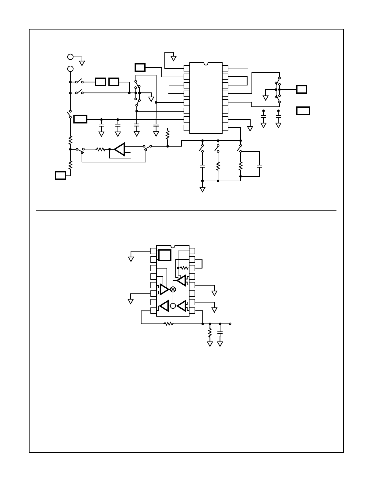
Test Circuit
L
MSR
H
K9
50Ω
50Ω
M1
K5
K6
- 15V
K7A
0.001
µF
1K
Specifications HA2546/883
G
16
15
14
13
12
11
10
9
K11K8
100Ω
G
G
V
V
V
V
V
ADJA
ADJC
ADJB
X+
X-
CC
Z-
Z+
K10
1K
V
V
GND
V
REF
ADJB
ADJA
V
V
V
V
OUT
50Ω
1
2
3
4
Y+
Y-
EE
DUT
5
6
7
8
25
µF
µF
M2
V1V2
10
1000
pF
K1
K2
1000
pF
K7B
For Detailed Information, Refer to HA-2546/883 Test Tech Brief
50pF
K3
K4
0.00110
V2
+15V
µFµF
Test Waveforms
LARGE AND SMALL SIGNAL RESPONSE TEST CIRCUIT
1
REF
2
NC
3
NC
4
NC
+
5
+
V
Y
V-
Y
6
-
7
8
50Ω
16
NC
15
14
+
13
+
V
12
-
11
V+
-
10
9
+
X
1K 50pF
V
OUT
X
+
-
Σ
Z
8-7
Spec Number 511050-883
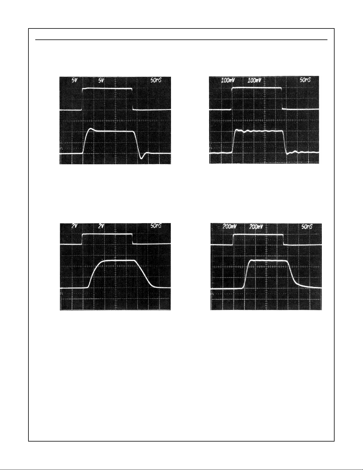
HA2546/883
Test Waveforms
(Continued)
VY LARGE SIGNAL RESPONSE
Vertical Scale: 5V/Div. Horizontal Scale: 50ns/Div.
+5V
IN 0
-5V
+5V
OUT 0
-5V
VX LARGE SIGNAL RESPONSE
Vertical Scale: 2V/Div. Horizontal Scale: 50ns/Div.
VY SMALL SIGNAL RESPONSE
Vertical Scale: 100mV/Div. Horizontal Scale: 50ns/Div.
100mV
IN 0
-100mV
100mV
OUT 0
-100mV
VX SMALL SIGNAL RESPONSE
Vertical Scale: 200mV/Div. Horizontal Scale: 50ns/Div.
IN
OUT
2V
5V
200mV
0
0
IN
0
500mV
OUT
0
8-8
Spec Number 511050-883
 Loading...