Intersil Corporation HA-2546 Datasheet

HA-2546
Data Sheet September 1998 File Number 2861.3
30MHz, Voltage Output, Two Quadrant
Analog Multiplier
The HA-2546 is a monolithic, high speed, two quadrant,
analog multiplier constructed in the Intersil Dielectrically
Isolated High Frequency Process. The HA-2546 has a
voltageoutput with a 30MHz signal bandwidth, 300V/µs slew
rate and a 17MHz control bandwidth. High bandwidth and
slew rate make this part an ideal component for use in video
systems. The suitability for precision video applications is
demonstrated further by the 0.1dB gain flatness to 5MHz,
1.6% multiplication error, -52dB feedthrough and differential
inputs with 1.2µA bias currents. The HA-2546 also has low
differential gain (0.1%) and phase (0.1 degree) errors.
The HA-2546 is well suited for AGC circuits as well as mixer
applications for sonar, radar, and medical imaging
equipment. The voltage output simplifies many designs by
eliminating the current to voltage conversion stage required
for current output multipliers. For MIL-STD-883 compliant
product, consult the HA-2546/883 datasheet.
Pinout
HA-2546
(PDIP, CERDIP, SOIC)
TOP VIEW
1
V
REF
V
B
YIO
V
A
YIO
+
V
Y
REF
2
3
4
X
5
GA AGND
16
GA C
15
GA B
14
+
V
X
13
-
V
X
12
Features
• High Speed Voltage Output . . . . . . . . . . . . . . . . . 300V/µs
• Low Multiplication error . . . . . . . . . . . . . . . . . . . . . . .1.6%
• Input Bias Currents. . . . . . . . . . . . . . . . . . . . . . . . . . 1.2µA
• Signal Input Feedthrough. . . . . . . . . . . . . . . . . . . . . -52dB
• Wide Signal Bandwidth . . . . . . . . . . . . . . . . . . . . . 30MHz
• Wide Control Bandwidth. . . . . . . . . . . . . . . . . . . . . 17MHz
• Gain Flatness to 5MHz. . . . . . . . . . . . . . . . . . . . . . 0.10dB
Applications
• Military Avionics
• Missile Guidance Systems
• Medical Imaging Displays
• Video Mixers
• Sonar AGC Processors
• Radar Signal Conditioning
• Voltage Controlled Amplifier
• Vector Generator
Ordering Information
TEMP.
PART NUMBER
HA1-2546-5 0 to 75 16 Ld CERDIP F16.3
HA3-2546-5 0 to 75 16 Ld PDIP E16.3
HA9P2546-5 0 to 65 16 Ld SOIC M16.3
RANGE (oC) PACKAGE
PKG.
NO.
V
V
Y
OUT
Y
6
-
7
V-
8
+
-
Z
Σ
1
V+
11
-
V
10
Z
VZ +
9
CAUTION: These devices are sensitive to electrostatic discharge; follow proper IC Handling Procedures.
1-888-INTERSIL or 321-724-7143
| Copyright © Intersil Corporation 1999

Simplified Schematic
V
BIAS
HA-2546
V
V +
BIAS
VX +
GA A
GA B
REF
GND
+
-
1.67kΩ
+
-
GA C
V
Y
V
VX -
+
YIO
VZ -VZ +
OUT
VY -
A
V
B
YIO
V -
2

HA-2546
Absolute Maximum Ratings Thermal Information
Voltage Between V+ and V-. . . . . . . . . . . . . . . . . . . . . . . . . . . . 35V
Differential Input Voltage . . . . . . . . . . . . . . . . . . . . . . . . . . . . . . . 6V
Output Current. . . . . . . . . . . . . . . . . . . . . . . . . . . . . . . . . . . . ±60mA
Operating Conditions
Temperature Range
HA3-2546-5, HA1-2546-5. . . . . . . . . . . . . . . . . . . . . 0oC to 75oC
HA9P2546-5. . . . . . . . . . . . . . . . . . . . . . . . . . . . . . . 0oC to 65oC
CAUTION: Stresses above those listed in “Absolute Maximum Ratings” may cause permanent damage to the device. This is a stress only rating and operation of the
device at these or any other conditions above those indicated in the operational sections of this specification is not implied.
NOTES:
1. θJA is measured with the component mounted on an evaluation PC board in free air.
Thermal Resistance (Typical, Note 1) θJA (oC/W) θJC (oC/W)
CERDIP Package. . . . . . . . . . . . . . . . . 75 20
PDIP Package . . . . . . . . . . . . . . . . . . . 86 N/A
SOIC Package . . . . . . . . . . . . . . . . . . . 96 N/A
Maximum Junction Temperature (CERDIP Package) . . . . . . . .175oC
Maximum Junction Temperature (Plastic Package) . . . . . . . .150oC
Maximum Storage Temperature Range. . . . . . . . . . -65oC to 150oC
Maximum Lead Temperature (Soldering 10s) . . . . . . . . . . . . 300oC
(SOIC - Lead Tips Only)
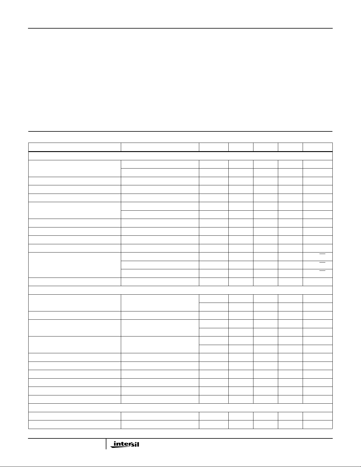
Electrical Specifications V
PARAMETER TEST CONDITIONS TEMP (
= ±15V, RL = 1kΩ, CL = 50pF, Unless Otherwise Specified
SUPPLY
o
C) MIN TYP MAX UNITS
MULTIPLIER PERFORMANCE
Multiplication Error (Note 2) 25 - 1.6 3 %
Full - 3.0 7 %
o
Multiplication Error Drift Full - 0.003 - %/
C
Differential Gain (Notes 3, 9) 25 - 0.1 0.2 %
Differential Phase (Notes 3, 9) 25 - 0.1 0.3 Degrees
Gain Flatness (Note 9) DC to 5MHz, V
5 MHz to 8MHz, V
= 2V 25 - 0.1 0.2 dB
X
= 2V 25 - 0.18 0.3 dB
X
Scale Factor Error Full - 0.7 5.0 %
1% Amplitude Bandwidth Error 25 - 6 - MHz
1% Vector Bandwidth Error 25 - 260 - kHz
THD + N (Note 4) 25 - 0.03 - %
Voltage Noise f
= 10Hz, VX = VY = 0V 25 - 400 - nV/√Hz
O
= 100Hz, VX = VY = 0V 25 - 150 - nV/√Hz
f
O
f
= 1kHz, VX = VY = 0V 25 - 75 - nV/√Hz
O
Common Mode Range 25 - ±9- V
SIGNAL INPUT, V
Y
Input Offset Voltage 25 - 3 10 mV
Full - 8 20 mV
Average Offset Voltage Drift Full - 45 - µV/oC
Input Bias Current 25 - 7 15 µA
Full - 10 15 µA
Input Offset Current 25 - 0.7 2 µA
Full - 1.0 3 µA
Input Capacitance 25 - 2.5 - pF
Differential Input Resistance 25 - 720 - kΩ
Small Signal Bandwidth (-3dB) V
Full Power Bandwidth (Note 5) V
= 2V 25 - 30 - MHz
X
= 2V 25 - 9.5 - MHz
X
Feedthrough Note 11 25 - -52 - dB
CMRR Note 6 Full 60 78 - dB
TRANSIENT RESPONSE (Note 10)
V
Y
Slew Rate V
= ±5V, VX = 2V 25 - 300 - V/µs
OUT
Rise Time Note 7 25 - 11 - ns
3

HA-2546
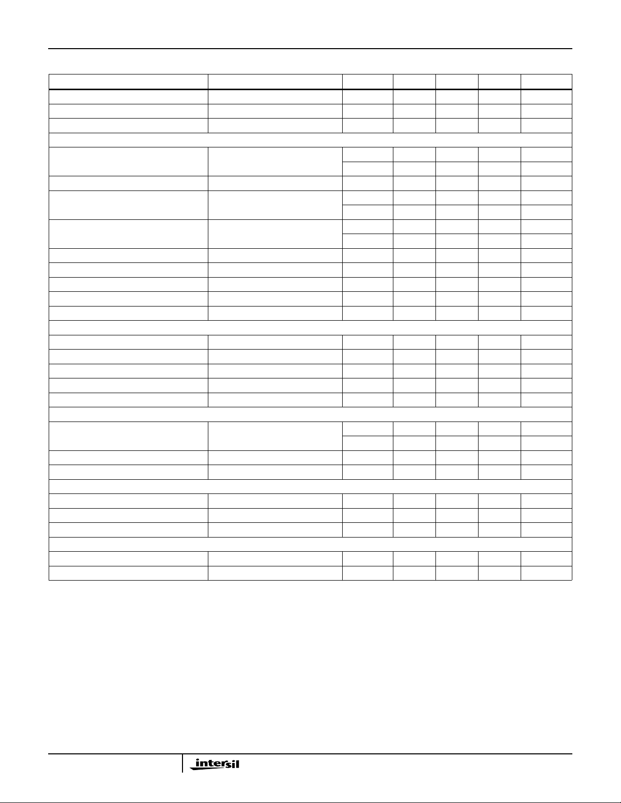
Electrical Specifications V
= ±15V, RL = 1kΩ, CL = 50pF, Unless Otherwise Specified (Continued)
SUPPLY
PARAMETER TEST CONDITIONS TEMP (oC) MIN TYP MAX UNITS
Overshoot Note 7 25 - 17 - %
Propagation Delay 25 - 25 - ns
Settling Time (To 0.1%) V
CONTROL INPUT, V
X
= ±5V, VX = 2V 25 - 200 - ns
OUT
Input Offset Voltage 25 - 0.3 2 mV
Full - 3 20 mV
Average Offset Voltage Drift Full - 10 - µV/
Input Bias Current 25 - 1.2 2 µA
Full - 1.8 5 µA
Input Offset Current 25 - 0.3 2 µA
Full - 0.4 3 µA
Input Capacitance 25 - 2.5 - pF
Differential Input Resistance 25 - 360 - kΩ
Small Signal Bandwidth (-3dB) V
= 5V, VX- = -1V 25 - 17 - MHz
Y
Feedthrough Note 12 25 - -40 - dB
Common Mode Rejection Ratio Note 13 25 - 80 - dB
TRANSIENT RESPONSE (Note 10)
V
X
Slew Rate Note 13 25 - 95 - V/µs
Rise Time Note 14 25 - 20 - ns
Overshoot Note 14 25 - 17 - %
Propagation Delay 25 - 50 - ns
Settling Time (To 0.1%) Note 13 25 - 200 - ns
CHARACTERISTICS
V
Z
Input Offset Voltage V
= VY = 0V 25 - 4 15 mV
X
Full - 8 20 mV
Open Loop Gain 25 - 70 - dB
Differential Input Resistance 25 - 900 - kΩ
OUTPUT CHARACTERISTICS
Output Voltage Swing V
= 2.5V, VY = ±5V Full - ±6.25 - V
X
Output Current Full ±20 ±45 - mA
Output Resistance 25 - 1 - Ω
POWER SUPPLY
PSRR Note 8 Full 58 63 - dB
Supply Current Full - 23 29 mA
NOTES:
2. Error is percent of full scale, 1% = 50mV.
= 3.58MHz/4.43MHz, VY = 300mV
3. f
O
4. fO = 10kHz, VY = 1V
RMS
, VX = 2V.
5. Full Power Bandwidth calculated by equation: .
6. VY = 0 to ±5V, VX = 2V.
7. V
= 0 to ±100mV, VX = 2V.
OUT
, 0 to 1VDC offset, VX = 2V.
P-P
Slew Rate
FPBW
---------------------------
2π V
PEAK
,V
PEAK
5V==
8. VS = ±12V to ±15V, VY = 5V, VX = 2V.
9. Guaranteed by characterization and not 100% tested.
10. See Test Circuit.
11. fO = 5MHz, VX = 0, VY = 200mV
12. fO = 100kHz, VY = 0, VX+ = 200mV
RMS
RMS
.
, VX- = -0.5V.
13. VX = 0 to 2V, VY = 5V.
14. VX = 0 to 200mV, VY = 5V.
o
C
4

Test Circuits and Waveforms
HA-2546
+5V
IN 0
1
REF
2
NC
3
NC
4
NC
5
+
V
Y
+
Y
-
6
7
V-
89
50Ω
+
-
Σ
16
NC
15
14
13
V
+
12
11
V+
10
-
+
1kΩ 50pF
X
V
OUT
+
X
-
Z
FIGURE 1. LARGE AND SMALL SIGNAL RESPONSE TEST CIRCUIT
100mV
IN 0
-5V
+5V
OUT 0
-5V
Vertical Scale: 5V/Div.; Horizontal Scale: 50ns/Div.
VY LARGE SIGNAL RESPONSE
2V
IN
0
5V
OUT
0
-100mV
100mV
OUT 0
-100mV
Vertical Scale: 100mV/Div.; Horizontal Scale: 50ns/Div.
VY SMALL SIGNAL RESPONSE
200mV
IN
0
500mV
OUT
0
Vertical Scale: 2V/Div.; Horizontal Scale: 50ns/Div.
VX LARGE SIGNAL RESPONSE
5
Vertical Scale: 200mV/Div.; Horizontal Scale: 50ns//Div.
VX SMALL SIGNAL RESPONSE
 Loading...