HA-2542
Data Sheet October 1999
70MHz, High Slew Rate, High Output
Current Operational Amplifier
The HA-2542 is a wideband, high slew rate, monolithic
operational amplifier featuring an outstanding combination of
speed, bandwidth, and output drive capability.
Utilizing the advantages of the Intersil D.I. technology this
amplifier offers 350V/µs slew rate, 70MHz gain bandwidth,
and ±100mA output current. Application of this device is
further enhanced through stable operation down to closed
loop gains of 2.
For additional flexibility, offset null and frequency
compensation controls are included in the HA-2542 pinout.
The capabilities of the HA-2542 are ideally suited for high
speed coaxial cable driver circuits where low gain and high
output drive requirements are necessary. With 5.5MHz full
power bandwidth, this amplifier is most suitable for high
frequency signal conditioning circuits and pulse video
amplifiers. Other applications utilizing the HA-2542
advantages include wideband amplifiers and fast samplehold circuits.
For more information on the HA-2542, please refer to
Application Note AN552 (Using the HA-2542), or Application
Note AN556 (Thermal Safe-Operating-Areas for High
Current Op Amps).
File Number 2899.3
Features
• Stable at Gains of 2 or Greater
• Gain Bandwidth . . . . . . . . . . . . . . . . . . . . . . . . . . . 70MHz
• High Slew Rate. . . . . . . . . . . . . . . . . . . . . . 300V/µs (Min)
• High Output Current. . . . . . . . . . . . . . . . . . . 100mA (Min)
• Power Bandwidth . . . . . . . . . . . . . . . . . . . . . 5.5MHz (Typ)
• Output Voltage Swing. . . . . . . . . . . . . . . . . . . ±10V (Min)
• Monolithic Bipolar Dielectric Isolation Construction
Applications
• Pulse and Video Amplifiers
• Wideband Amplifiers
• Coaxial Cable Drivers
• Fast Sample-Hold Circuits
• High Frequency Signal Conditioning Circuits
Pinout
HA-2542
(PDIP, CERDIP)
TOP VIEW
For a lower power version of this product, please see
the HA-2842 data sheet.
Ordering Information
TEMP.
PART NUMBER
HA1-2542-5 0 to 75 14 Ld CERDIP F14.3
HA3-2542-5 0 to 75 14 Ld PDIP E14.3
RANGE (oC) PACKAGE
PKG.
NO.
NC
NC
BAL
-IN
+IN
NC
1
2
3
4
-
+
5
6
V-
7
14
13
12
11
10
9
8
NC
BAL
COMP
V+
OUT
NC
NC
1
CAUTION: These devices are sensitive to electrostatic discharge; follow proper IC Handling Procedures.
1-888-INTERSIL or 321-724-7143
| Copyright © Intersil Corporation 1999

HA-2542
Absolute Maximum Ratings Thermal Information
Supply Voltage (Between V+ and V- Terminals) . . . . . . . . . . . . .35V
Differential Input Voltage . . . . . . . . . . . . . . . . . . . . . . . . . . . . . . . .6V
Output Current. . . . . . . . . . . . . . . . 50mA Continuous, 125mA
PEAK
Operating Conditions
Temperature Range
HA-2542-5 . . . . . . . . . . . . . . . . . . . . . . . . . . . . . . . . 0oCto75oC
CAUTION: Stresses above those listed in “Absolute Maximum Ratings” may cause permanent damage to the device. This is a stress only rating and operation of the
device at these or any other conditions above those indicated in the operational sections of this specification is not implied.
NOTES:
1. Maximum power dissipation with load conditions must be designed to maintain the maximum junction temperature below 175oC for ceramic
packages, and below 150oC for plastic packages. By using Application Note AN556 on Safe Operating Area equations, along with the thermal
resistances, proper load conditions can be determined. Heatsinking will be required in many applications. See the “Application Information”
section to determine if heat sinking is required for your application.
2. θJA is measured with the component mounted on an evaluation PC board in free air.
Thermal Resistance (Typical, Note 2) θJA (oC/W) θJC (oC/W)
CERDIP Package. . . . . . . . . . . . . . . . . 75 20
PDIP Package . . . . . . . . . . . . . . . . . . . 95 N/A
Maximum Junction Temperature (Note 1, Hermetic Packages) . 175oC
Maximum Junction Temperature (Plastic Package) . . . . . . . .150oC
Maximum Storage Temperature Range. . . . . . . . . . -65oC to 150oC
Maximum Lead Temperature (Soldering 10s) . . . . . . . . . . . . .300oC
Electrical Specifications V
PARAMETER
INPUT CHARACTERISTICS
Offset Voltage 25 - 5 10 mV
Average Offset Voltage Drift Full - 14 - µV/oC
Bias Current 25 - 15 35 µA
Average Bias Current Drift Full - 45 - nA/oC
Offset Current 25 - 1 7 µA
Input Resistance 25 - 100 - kΩ
Input Capacitance 25 - 1 - pF
Common Mode Range Full ±10 - - V
Input Noise Voltage 0.1Hz to 100Hz 25 - 2.2 - µV
Input Noise Density f = 1kHz, RG = 0Ω 25 - 10 - nV/√Hz
Input Noise Current Density f = 1kHz, RG = 0Ω 25 - 3 - pA/√Hz
TRANSFER CHARACTERISTICS
Large Signal Voltage Gain VO = ±10V 25 10 30 - kV/V
Common Mode Rejection Ratio VCM = ±10V Full 70 100 - dB
Minimum Stable Gain 25 2 - - V/V
Gain Bandwidth Product AV = 100 25 - 70 - MHz
OUTPUT CHARACTERISTICS
Output Voltage Swing Full ±10 ±11 - V
Output Current (Note 3) 25 100 - - mA
Output Resistance 25 - 5 - Ω
= ±15V, RL = 1kΩ, CL≤ 10pF, Unless Otherwise Specified
SUPPLY
TEST
CONDITIONS
HA-2542-5
TEMP.
o
(
C)
Full - 8 20 mV
Full - 26 50 µA
Full - - 9 µA
Full 5 20 - kV/V
0oC TO 75oC
UNITSMIN TYP MAX
P-P
2

HA-2542
Electrical Specifications V
= ±15V, RL = 1kΩ, CL≤ 10pF, Unless Otherwise Specified (Continued)
SUPPLY
HA-2542-5
0oC TO 75oC
UNITSMIN TYP MAX
PARAMETER
Full Power Bandwidth (Note 4) V
TEST
CONDITIONS
= 10V 25 4.7 5.5 - MHz
PEAK
TEMP.
(oC)
Differential Gain (Note 5) 25 - 0.1 - %
Differential Phase (Note 5) 25 - 0.2 - Degree
Harmonic Distortion (Note 7) 25 - <0.04 - %
TRANSIENT RESPONSE (Note 6)
Rise Time 25 - 4 - ns
Overshoot 25 - 25 - %
Slew Rate 25 300 350 - V/µs
Settling Time 10V Step to 0.1% 25 - 100 - ns
10V Step to 0.01% 25 - 200 - ns
POWER SUPPLY CHARACTERISTICS
Supply Current 25 - 30 - mA
Full - 31 40 mA
Power Supply Rejection Ratio VS = ±5V to ±15V Full 70 79 - dB
NOTES:
3. RL = 50Ω, VO = ±5V, Output duty cycle must be reduced for I
4. Full Power Bandwidth guaranteed based on slew rate measurement using: .
> 50mA (e.g. ≤50% duty cycle for 100mA).
OUT
FPBW
Slew Rate
---------------------------- -=
2πV
PEAK
5. Differential gain and phase are measured at 5MHz with a 1V differential input voltage.
6. Refer to Test Circuits section of this data sheet.
7. VIN = 1V
; f = 10kHz; AV = 10.
RMS
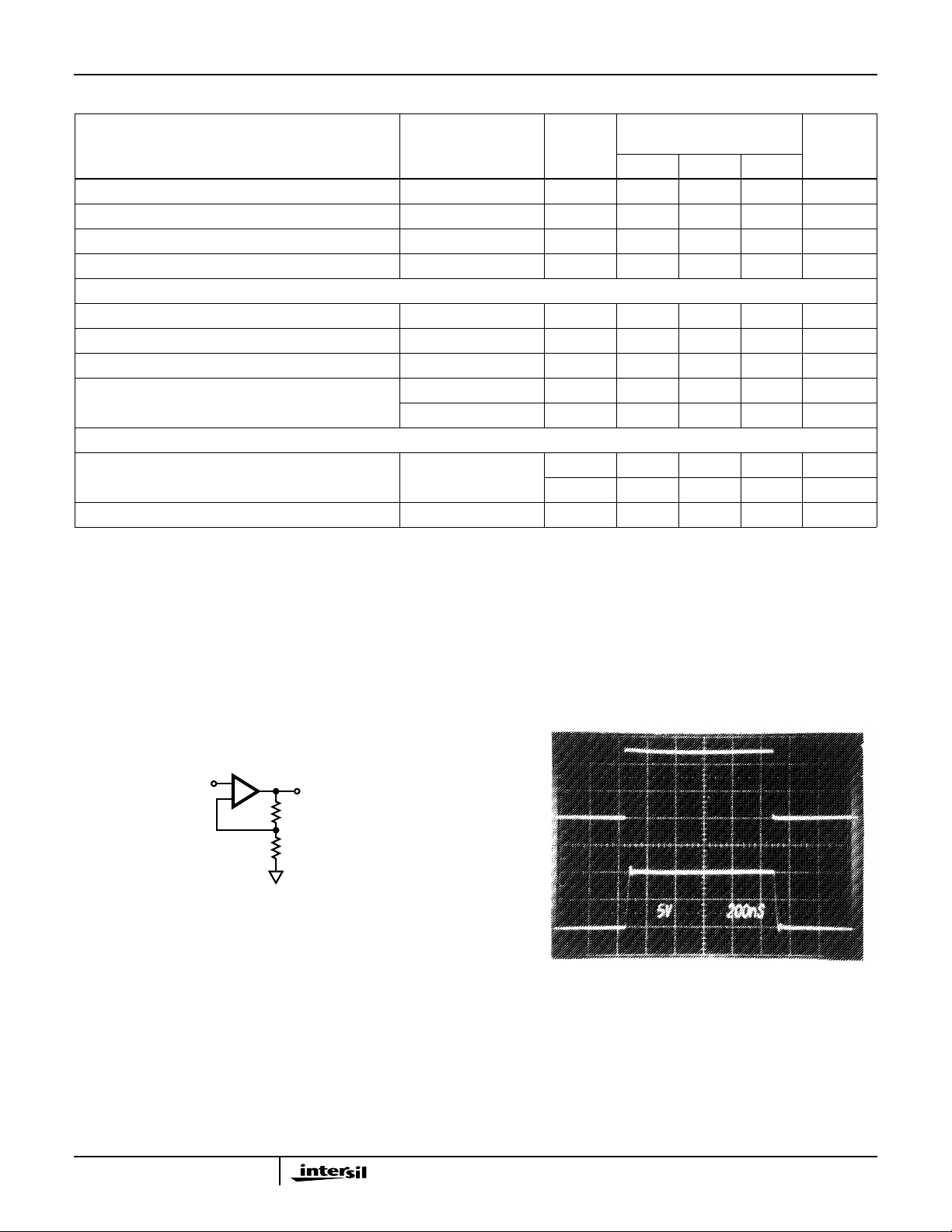
Test Circuits and Waveforms
IN
+
-
NOTES:
8. VS = ±15V.
9. AV = +2.
10. CL≤ 10pF.
TEST CIRCUIT LARGE SIGNAL RESPONSE
OUT
500Ω
500Ω
V
V
OUT
IN
Vertical Scale: VIN = 2.0V/Div., V
= 5.0V/Div.
OUT
Horizontal Scale: 200ns/Div.
3

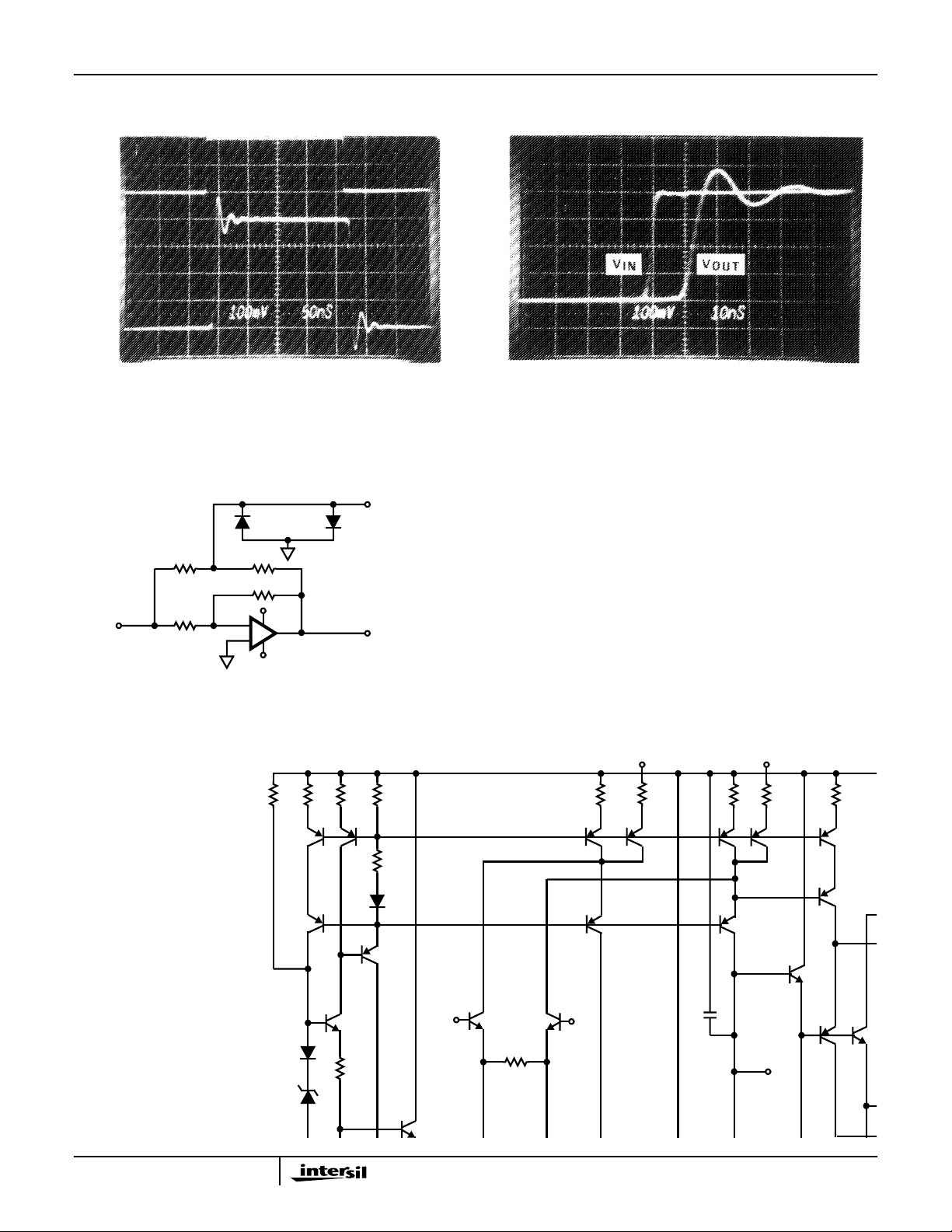
Test Circuits and Waveforms (Continued)
V
IN
V
OUT
HA-2542
Vertical Scale: 100mV/Div.
Horizontal Scale: 50ns/Div.
SMALL SIGNAL RESPONSE PROPAGATION DELAY
2.5kΩ
V
IN
500Ω
5kΩ
1kΩ
-
+
V+
V-
SETTLING TIME TEST CIRCUIT (SEE NOTES 11 - 15.)
Schematic Diagram
R11R7R8R
Q
P15QP13
SETTLING
POINT
V
OUT
9
R
14
Vertical Scale: 100mV/Div.
Horizontal Scale: 10ns/Div.
VS= ±15V,RL=1kΩ. Propagation delay variance
is negligible over full temperature range.
NOTES:
11. AV = -2.
12. Feedback and summing resistors must be matched (0.1%).
13. HP5082-2810 clipping diodes recommended.
14. Tektronix P6201 FET probe used at settling point.
15. For 0.01% settling time, heat sinking is suggested to reduce
thermal effects and an analog ground plane with supply
decoupling is suggested to minimize ground loop errors.
BAL BAL
R
R
10
5kΩ
Q
25
P34
75Ω
Q
P14
R
75Ω
Q
12
P16
R
5kΩ
Q
26
P35
Q
R
P33
15
Q
N12
Q
-IN
P5
C
Q
P7
1
COMP
Q
P31
Q
P11
Q
Q
N42
Q
N44
R
18
D
Z45
Q
N18
+IN
Q
N1
N2
R
6
Q
P32
Q
N23
Q
P36
Q
N
4
 Loading...