Intersil Corporation HA-2541 Datasheet

HA-2541
Data Sheet September 1998 File Number 2898.3
40MHz, Fast Settling, Unity Gain Stable,
Operational Amplifier
The HA-2541 is the first unity gain stable monolithic
operational amplifier to achieve 40MHz unity gain
bandwidth. A major addition to the Intersil series of high
speed, wideband op amps, the HA-2541 is designed for
video and pulse applications requiring stable amplifier
response at low closed loop gains.
The uniqueness of the HA-2541 is that its slew rate and
bandwidth characteristics are specified at unity gain.
Historically, high slew rate, wide bandwidth and unity gain
stability have been incompatible features for a monolithic
operational amplifier. But features such as 250V/µs slew rate
and 40MHz unity gain bandwidth clearly show that this is not
the case for the HA-2541. These features , along with 90ns
settling time to 0.1%, make this product an excellent choice
for high speed data acquisition systems.
MIL-STD-883 product and data sheets are available upon
request, Intersil AnswerFAX (407-724-7800) document
#3698.
For further application suggestions on the HA-2541, please
refer to Application Note AN550 (Using the HA-2541), and
Application Note AN556 (Thermal Safe Operating Areas for
High Current Operational Amplifiers), Intersil AnswerFAX
(407-724-7800) document #9550 and 9556. Also see
‘Applications’ in this data sheet.
Features
• Unity Gain Bandwidth. . . . . . . . . . . . . . . . . . . . . . . 40MHz
• High Slew Rate. . . . . . . . . . . . . . . . . . . . . . . . . . . 250V/µs
• Low Offset Voltage . . . . . . . . . . . . . . . . . . . . . . . . . 0.8mV
• Fast Settling Time (0.1%). . . . . . . . . . . . . . . . . . . . . 90ns
• Power Bandwidth . . . . . . . . . . . . . . . . . . . . . . . . . . . 4MHz
• Output Voltage Swing (Min) . . . . . . . . . . . . . . . . . . . ±10V
• Unity Gain Stability
• Monolithic Bipolar Dielectric Isolation Construction
Applications
• Pulse and Video Amplifiers
• Wideband Amplifiers
• High Speed Sample-Hold Circuits
• Fast, Precise D/A Converters
• High Speed A/D Input Buffer
Ordering Information
PART
NUMBER
HA1-2541-5 0 to 75 14 Ld CERDIP F14.3
TEMP.
RANGE (oC) PACKAGE PKG. NO.
For a lower power version of this product, please see
the HA-2841 data sheet.
1
CAUTION: These devices are sensitive to electrostatic discharge; follow proper IC Handling Procedures.
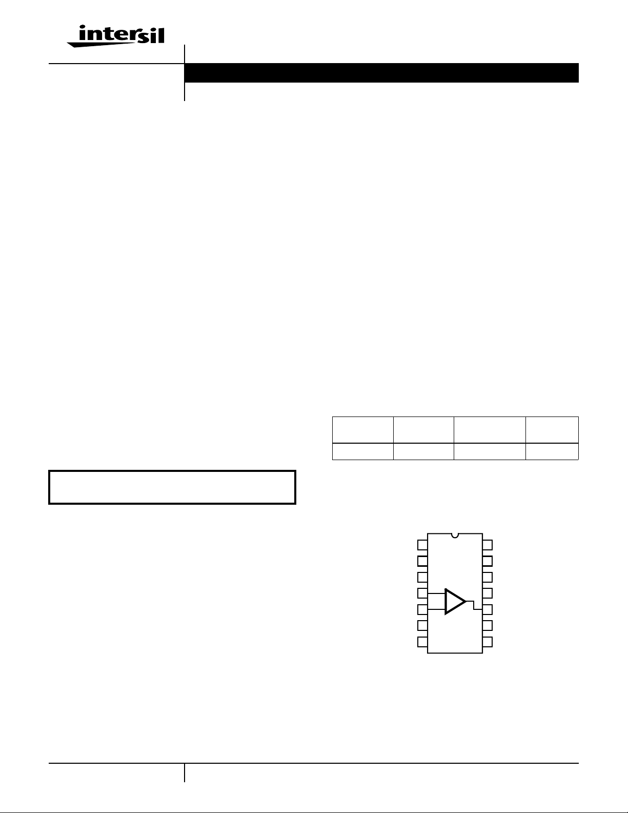
Pinout
NC
1
2
NC
3
BAL
4
-IN
5
+IN
6
V-
7
NC
1-888-INTERSIL or 321-724-7143
HA1-2541
(CERDIP)
TOP VIEW
14
NC
13
NC
12
BAL
11
-
+
| Copyright © Intersil Corporation 1999
V+
10
OUT
9
NC
8
NC

HA-2541
Absolute Maximum Ratings Thermal Information
Voltage Between V+ and V- Terminals. . . . . . . . . . . . . . . . . . . . 35V
Differential Input Voltage . . . . . . . . . . . . . . . . . . . . . . . . . . . . . . . 6V
Peak Output Current . . . . . . . . . . . . . . . . . . . . . . . . . . . . . . . . 50mA
Continuous Output Current . . . . . . . . . . . . . . . . . . . . . . . 28mA
RMS
Operating Conditions
Temperature Range
HA-2541-5 . . . . . . . . . . . . . . . . . . . . . . . . . . . . . . . . 0oC to 75oC
CAUTION: Stresses above those listed in “Absolute Maximum Ratings” may cause permanent damage to the device. This is a stress only rating and operation of the
device at these or any other conditions above those indicated in the operational sections of this specification is not implied.
NOTES:
1. Maximum power dissipation with load conditions must be designed to maintain the maximum junction temperature below 175oC. By using Application Note AN556 on Safe Operating Area equations, along with the thermal resistances, proper load conditions can be determined. Heat
sinking is recommended above 75oC.
2. θJA is measured with the component mounted on an evaluation PC board in free air.
Thermal Resistance (Typical, Note 2) θJA (oC/W) θJC (oC/W)
CERDIP Package. . . . . . . . . . . . . . . . . 75 20
Maximum Junction Temperature (Note 1) . . . . . . . . . . . . . . . .175oC
Maximum Storage Temperature Range. . . . . . . . . . -65oC to 150oC
Maximum Lead Temperature (Soldering 10s) . . . . . . . . . . . . 300oC
Electrical Specifications V
PARAMETER
INPUT CHARACTERISTICS
Offset Voltage 25 - 1 2 mV
Average Offset Voltage Drift Full - 9 - µV/oC
Bias Current 25 - 11 35 µA
Average Bias Current Drift Full - 85 - nA/oC
Offset Current 25 - 1 7 µA
Input Resistance 25 - 100 - kΩ
Input Capacitance 25 - 1 - pF
Common Mode Range Full ±10 ±11 - V
Input Noise Voltage f = 1kHz, Rg = 0Ω 25 - 10 - nV/√Hz
Input Noise Current f = 1kHz, Rg = 0Ω 25 - 4 - pA/√Hz
TRANSFER CHARACTERISTICS
Large Signal Voltage Gain VO = ±10V 25 10 16 - kV/V
Common Mode Rejection Ratio VCM = ±10V Full 70 90 - dB
Minimum Stable Gain 25 1 - - V/V
Unity Gain Bandwidth VO = 90mV 25 - 40 - MHz
OUTPUT CHARACTERISTICS
Output Voltage Swing RL = 1kΩ Full ±10 ±11 - V
Output Current RL = 1kΩ 25 ±10 ±15 - mA
Output Resistance 25 - 2 - Ω
Full Power Bandwidth (Note 3) VP = 10V 25 3 4 - MHz
Differential Gain Note 4 25 - 0.1 - %
Differential Phase Note 4 25 - 0.2 - Degrees
Harmonic Distortion Note 6 25 - <0.01 - %
= ±15V, RL = 1kΩ, CL≤ 10pF, Unless Otherwise Specified
SUPPLY
TEST
CONDITIONS
TEMP
o
(
Full - - 6 mV
Full - - 50 µA
Full - - 9 µA
Full 5 - - kV/V
C)
HA-2541-5
0oC TO 75oC
UNITSMIN TYP MAX
2

HA-2541
Electrical Specifications V
= ±15V, RL = 1kΩ, CL≤ 10pF, Unless Otherwise Specified (Continued)
SUPPLY
HA-2541-5
0oC TO 75oC
UNITSMIN TYP MAX
PARAMETER
TEST
CONDITIONS
TEMP
o
(
C)
TRANSIENT RESPONSE (Note 5)
Rise Time 25 - 4 - ns
Overshoot 25 - 40 - %
Slew Rate 25 200 250 - V/µs
Settling Time 10V Step To 0.1% 25 - 90 - ns
10V Step T o 0.01% 25 - 175 - ns
POWER REQUIREMENTS
Supply Current 25 - 29 - mA
Full - - 40 mA
Power Supply Rejection Ratio VS = ±5V to ±15V Full 70 78 - dB
NOTES:
3. Full Power Bandwidth guaranteed based on slew rate measurement using: .
FPBW
4. Differential Gain and Phase are measured with a 1V differential voltage at 5MHz.
Slew Rate
---------------------------- -=
2πV
PEAK
5. Refer to Test Circuits section of this data sheet.
6. f = 10kHz; AV = 5; VO = 14V
P-P.
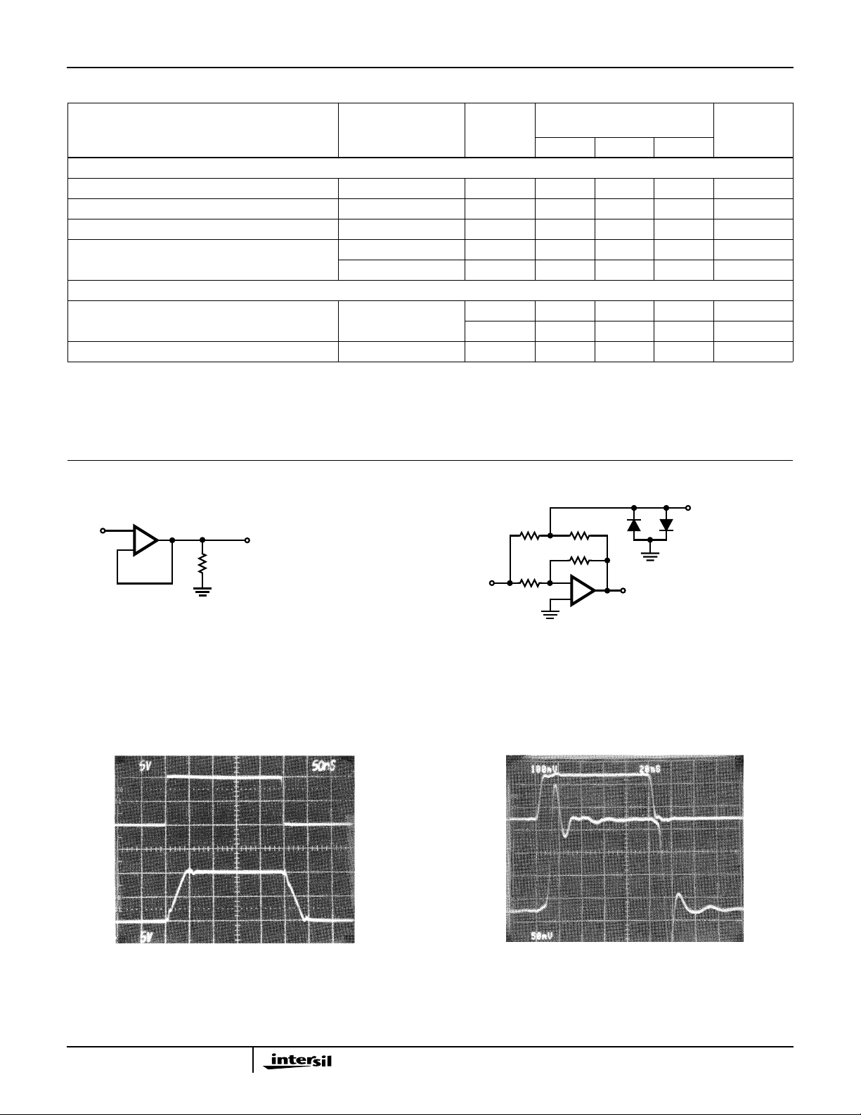
Test Circuits and Waveforms
5kΩ5kΩ
2kΩ
-
+
V
OUT
V
IN
+
-
1kΩ
V
OUT
NOTES:
7. VS = ±15V.
8. AV = +1.
9. CL≤ 10pF.
V
IN
2kΩ
NOTES:
10. AV = -1.
11. Feedback and summing resistor ratios should be 0.1% matched.
12. HP5082-2810 clipping diodes recommended.
13. Tektronix P6201 FET probe used at settling point.
FIGURE 1. TRANSIENT RESPONSE TEST CIRCUIT FIGURE 2. SETTLING TIME TEST CIRCUIT
V
V
V
OUT
IN
0V
0V
V
IN
OUT
SETTLING
POINT
0V
0V
Vertical Scale: 5V/Div.
Horizontal Scale: 50ns/Div.
Vertical Scale: VIN = 100mV/Div., V
Horizontal Scale: 20ns/Div.
LARGE SIGNAL RESPONSE SMALL SIGNAL RESPONSE
3
= 50mV/Div.
OUT
 Loading...