HA-2540
Data Sheet September 1998 File Number 2897.3
400MHz, Fast Settling Operational
Amplifier
The Intersil HA-2540 is a wideband, very high slew rate,
monolithic operationalamplifierfeaturingsuperiorspeed and
bandwidth characteristics. Bipolar construction coupled with
dielectric isolation allows this truly differential device to
deliver outstanding performance in circuits where closed
loop gain is 10 or greater. Additionally, the HA-2540 has a
drive capability of ±10V into a 1kΩ load. Other desirable
characteristics include low input voltage noise, low offset
voltage, and fast settling time.
A 400V/µs slew rate ensures high performance in video and
pulse amplification circuits, while the 400MHz gainbandwidth product is ideally suited for wideband signal
amplification. A settling time of 140ns also makes the
HA-2540 an excellent selection for high speed Data
Acquisition Systems.
Refer to Application Note AN541 and Application Note
AN556 for more information on High Speed Op Amp
applications. HA-2540/883 MIL-STD-883 data sheet is
available on request.
For a lower power version of this product, please see
the HA-2850 datasheet.
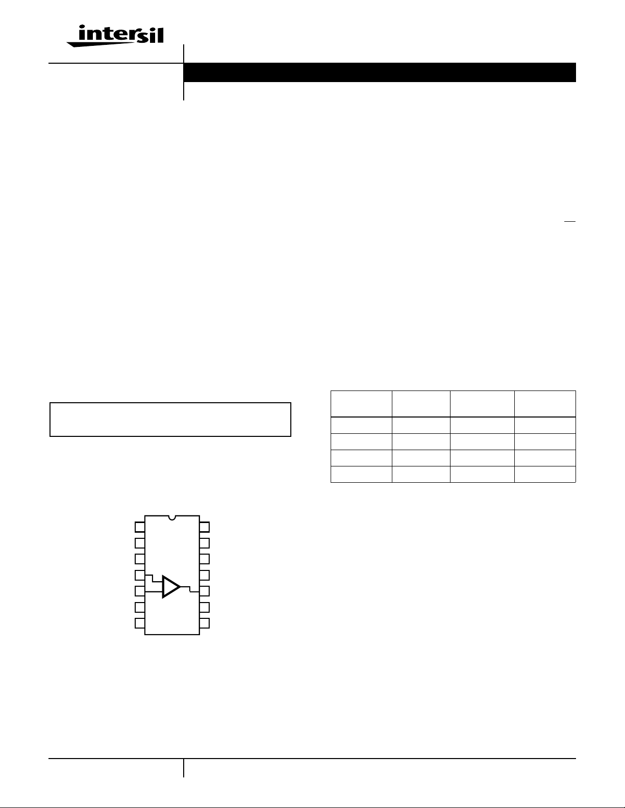
Pinout
HA-2540
(CERDIP, PDIP)
TOP VIEW
Features
• Very High Slew Rate . . . . . . . . . . . . . . . . . . . . . . 400V/µs
• Fast Settling Time. . . . . . . . . . . . . . . . . . . . . . . . . . .140ns
• Wide Gain Bandwidth (A
≥ 10) . . . . . . . . . . . . . . 400MHz
V
• Power Bandwidth . . . . . . . . . . . . . . . . . . . . . . . . . . . 6MHz
• Low Offset Voltage . . . . . . . . . . . . . . . . . . . . . . . . . . . 8mV
• Input Voltage Noise . . . . . . . . . . . . . . . . . . . . . . .6nV/√
Hz
• Output Voltage Swing. . . . . . . . . . . . . . . . . . . . . . . . ±10V
• Monolithic Bipolar Construction
Applications
• Pulse and Video Amplifiers
• Wideband Amplifiers
• High Speed Sample-Hold Circuits
• Fast, Precise D/A Converters
Ordering Information
PART
NUMBER
HA1-2540-2 -55 to 125 14 Ld CERDIP F14.3
HA1-2540-5 0 to 75 14 Ld CERDIP F14.3
HA3-2540-5 0 to 75 14 Ld PDIP E14.3
HA3-2540C-5 0 to 75 14 Ld PDIP E14.3
TEMP.
RANGE (oC) PACKAGE PKG. NO.
NC
NC
NC
-IN
+IN
NC
1
2
3
4
-
+
5
6
V-
7
14
NC
13
NC
12
NC
11
V+
10
OUTPUT
9
NC
8
NC
1
CAUTION: These devices are sensitive to electrostatic discharge; follow proper IC Handling Procedures.
1-888-INTERSIL or 321-724-7143
| Copyright © Intersil Corporation 1999

HA-2540
Absolute Maximum Ratings Thermal Information
Voltage Between V+ and V- Terminals. . . . . . . . . . . . . . . . . . . . 35V
Differential Input Voltage . . . . . . . . . . . . . . . . . . . . . . . . . . . . . . . 6V
Output Current. . . . . . . . . . . . . . 33mA
Continuous, 50mA
RMS
PEAK
Operating Conditions
Temperature Range
HA-2540-2 . . . . . . . . . . . . . . . . . . . . . . . . . . . . . . -55oC to 125oC
HA-2540/2540C-5 . . . . . . . . . . . . . . . . . . . . . . . . . . 0oC to 75oC
CAUTION: Stresses above those listed in “Absolute Maximum Ratings” may cause permanent damage to the device. This is a stress only rating and operation of the
device at these or any other conditions above those indicated in the operational sections of this specification is not implied.
NOTES:
1. Maximumpower dissipation with load conditions mustbe designed to maintain themaximum junction temperature below 175oC forthe ceramic
package, and below150oC for theplastic package. By using Application Note AN556on Safe Operating Area Equations, along withthe thermal
resistances, proper load conditions can be determined. Heat sinking is recommended above 75oC.
2. θJA is measured with the component mounted on an evaluation PC board in free air.
Thermal Resistance (Typical, Note 2) θJA (oC/W) θJC (oC/W)
CERDIP Package. . . . . . . . . . . . . . . . . 75 20
PDIP Package . . . . . . . . . . . . . . . . . . . 107 N/A
Maximum Internal Power Dissipation (Note 1)
Maximum Junction Temperature (Ceramic Package) . . . . . . 175oC
Maximum Junction Temperature (Plastic Package). . . . . . . . .150oC
Maximum Storage Temperature Range. . . . . . . . . . -65oC to 150oC
Maximum Lead Temperature (Soldering 10s) . . . . . . . . . . . . 300oC
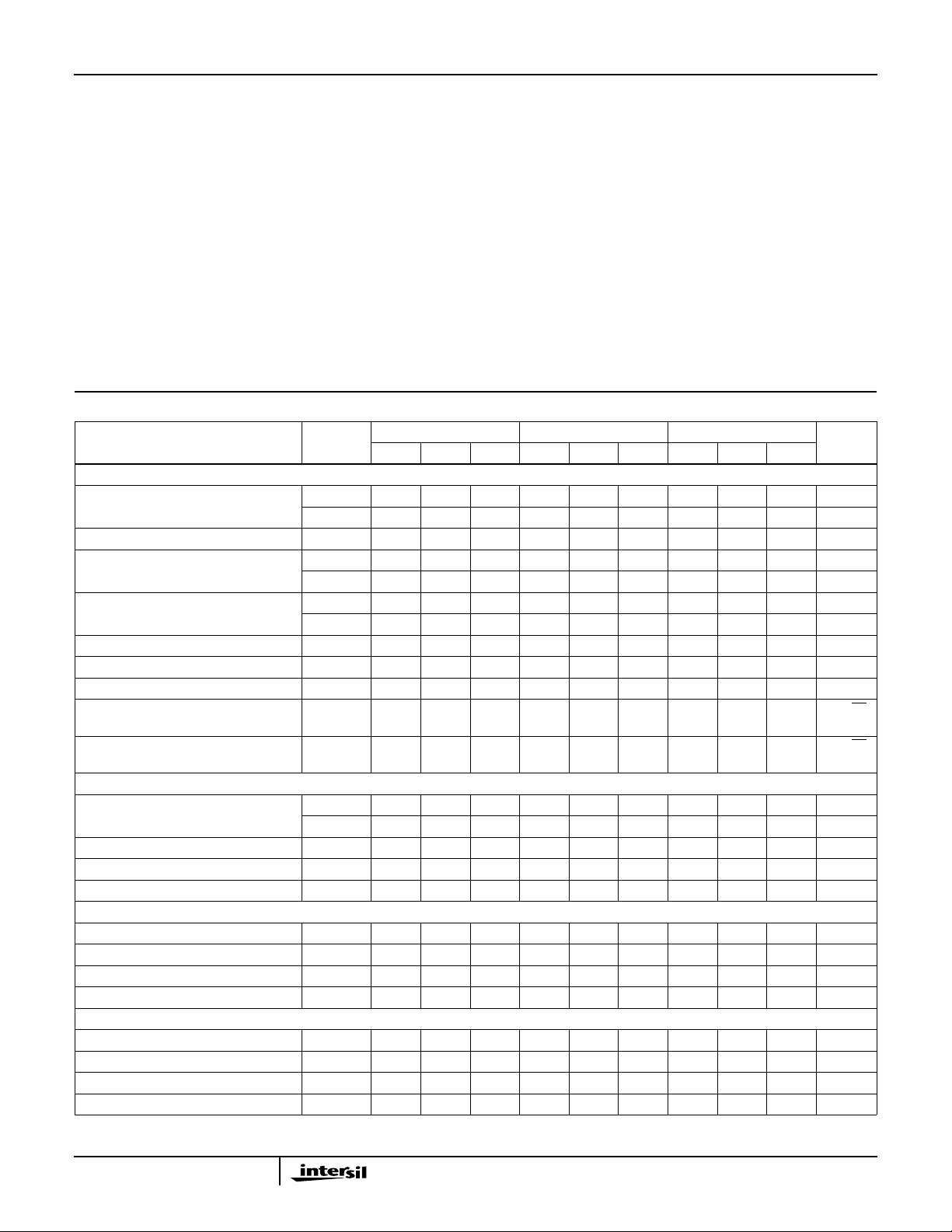
Electrical Specifications V
PARAMETER
INPUT CHARACTERISTICS
Offset Voltage 25 - 8 10 - 8 15 - 8 15 mV
Average Offset Voltage Drift Full - 20 - - 20 - - 20 - µV/
Bias Current 25 - 5 20 - 5 20 - 5 20 µA
Offset Current 25 - 1 6 - 1 6 - 1 6 µA
Input Resistance 25 - 10 - - 10 - - 10 - kΩ
Input Capacitance
Common Mode Range Full ±10 - - ±10 - - ±10 - - V
Input Noise Current (f = 1kHz,
R
SOURCE
Input Noise Voltage (f = 1kHz,
R
SOURCE
TRANSFER CHARACTERISTICS
Large Signal Voltage Gain (Note 3) 25 10 15 - 10 15 - 7 10 - kV/V
Common-Mode Rejection Ratio (Note 4) Full 60 72 - 60 72 - 60 72 - dB
Minimum Stable Gain 25 10 - - 10 - - 10 - - V/V
Gain Bandwidth Product (Notes 5, 6) 25 - 400 - - 400 - - 400 - MHz
OUTPUT CHARACTERISTICS
Output Voltage Swing (Notes 3, 10) Full ±10 - - ±10 - - ±10 - - V
Output Current (Note 3) 25 ±10 ±20 - ±10 ±20 - ±10 ±20 - mA
Output Resistance 25 - 30 - - 30 - - 30 - Ω
Full Power Bandwidth (Notes 3, 7) 25 5.5 6 - 5.5 6 - 5.5 6 - MHz
TRANSIENT RESPONSE (Note 8)
Rise Time 25 - 14 - - 14 - - 14 - ns
Overshoot 25 - 5 - - 5 - - 5 - %
Slew Rate 25 320 400 - 320 400 - 320 400 - V/µs
Settling Time: 10V Step to 0.1% 25 - 140 - - 140 - - 140 - ns
= 0Ω)
= 0Ω)
= ±15V, RL = 1kΩ, CL < 10pF, Unless Otherwise Specified
SUPPLY
TEMP
(oC)
Full - 13 15 - 13 20 - 13 20 mV
Full - - 25 - - 25 - - 25 µA
Full - - 8 - - 8 - - 8 µA
25
25 - 6 - - 6 - - 6 - pA/√Hz
25 - 6 - - 6 - - 6 - nV/√Hz
Full 5 - - 5 - - 5 - - kV/V
HA-2540-2 HA-2540-5 HA-2540C-5
-1- -1- -1-pF
UNITSMIN TYP MAX MIN TYP MAX MIN TYP MAX
o
C
2

HA-2540
Electrical Specifications V
PARAMETER
= ±15V, RL = 1kΩ, CL < 10pF, Unless Otherwise Specified (Continued)
SUPPLY
TEMP
HA-2540-2 HA-2540-5 HA-2540C-5
(oC)
UNITSMIN TYP MAX MIN TYP MAX MIN TYP MAX
POWER REQUIREMENTS
Supply Current Full - 20 25 - 20 25 - 20 25 mA
Power Supply Rejection Ratio (Note 9) Full 60 70 - 60 70 - 60 70 - dB
NOTES:
= 1kΩ, VO= ±10V.
3. R
L
4. VCM = ±10V.
5. VO = 90mV.
6. AV = 10.
7. Full power bandwidth guaranteed based on slew rate measurement using: .
FPBW
8. Refer to Test Circuits section of the data sheet.
9. V
= +5V, -15V and +15V, -5V.
SUPPLY
Slew Rate
---------------------------=
2πV
PEAK
10. Guaranteed range for output voltage is ±10V. Functional operation outside of this range is not guaranteed.
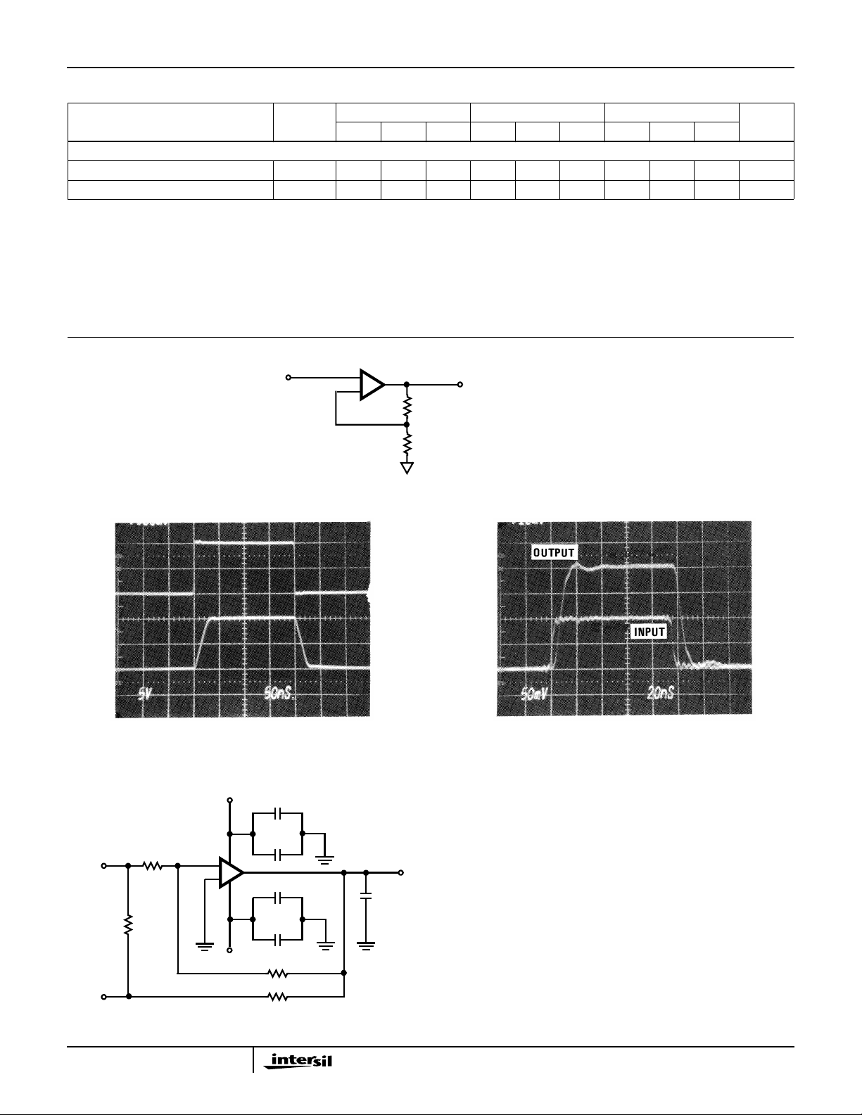
Test Circuits and Waveforms
V
IN
+
-
900
V
OUT
NOTES:
100
11. AV = +10.
12. CL≤ 10pF.
A
B
INPUT
500Ω
SETTLE
POINT
FIGURE 1. LARGE AND SMALL SIGNAL RESPONSE TEST CIRCUIT
Vertical Scale: A = 0.5V/Div., B = 5.0V/Div.
Horizontal Scale: 50ns/Div.
Vertical Scale: Input = 10mV/Div.; Output = 50mV/Div.
Horizontal Scale: 20ns/Div.
LARGE SIGNAL RESPONSE SMALL SIGNAL RESPONSE
V+
0.001µF
NOTES:
13. AV = -10.
200Ω
1µF
-
+
0.001µF
1µF
V-
2kΩ
5kΩ
OUTPUT
PROBE
MONITOR
14. Load Capacitance should be less than 10pF. Turn on time delay
typically 4ns.
15. Itis recommended that resistors be carbon composition and the
feedback and summing network ratios be matched to 0.1%.
16. SETTLEPOINT (Summing Node) capacitance should be less
than 10pF. For optimum settling time results, it is recommended
that the test circuit be constructed directly onto the device pins. A
Tektronix 568 SamplingOscilloscope withS-3A sampling headsis
recommended as a settle point monitor.
FIGURE 2. SETTLING TIME TEST CIRCUIT
3
 Loading...