Intersil Corporation HA-2505 Datasheet

HA-2505
Data Sheet May 1999
12MHz, High Input Impedance,
Operational Amplifier
HA-2505 is an operational amplifier whose design is
optimized to deliver excellent slew rate, bandwidth, and
settling time specifications. The outstanding dynamic
features of this internally compensated device are
complemented with low offset voltage and offset current.
This dielectrically isolated amplifier is ideally suited for
applications such as data acquisition, RF, video, and pulse
conditioning circuits. Slew rates of ±30V/µs and 330ns
(0.1%) settling time make this device an excellent
component in fast, accurate data acquisition and pulse
amplification designs. 12MHz small signal bandwidth and
500kHz power bandwidth make this device well suited to RF
and video applications. With 2mV typical offset voltage plus
offset trim capability and 10nA offset current, HA-2505 is
particularly useful in signal conditioning designs.
The gain and offset voltage figures of the HA-2505 are
optimized by internal component value changes while the
similar design of the HA-2515 is maximized for slew rate.
MIL-STD-883 product and data sheets are available upon
request.
File Number 2890.5
Features
• Slew Rate. . . . . . . . . . . . . . . . . . . . . . . . . . . . . . . . 30V/µs
• Fast Settling . . . . . . . . . . . . . . . . . . . . . . . . . . . . . . 330ns
• Full Power Bandwidth. . . . . . . . . . . . . . . . . . . . . . 500kHz
• Gain Bandwidth . . . . . . . . . . . . . . . . . . . . . . . . . . . 12MHz
• High Input Impedance . . . . . . . . . . . . . . . . . . . . . . 50MΩ
• Low Offset Current. . . . . . . . . . . . . . . . . . . . . . . . . . 10nA
• Internally Compensated For Unity Gain Stability
Applications
• Data Acquisition Systems
• RF Amplifiers
• Video Amplifiers
• Signal Generators
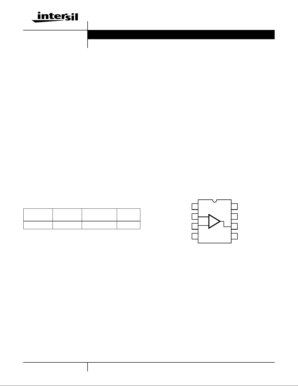
Pinout
HA-2505 (PDIP)
TOP VIEW
Ordering Information
PART
NUMBER
HA3-2505-5 0 to 75 8 Ld PDIP E8.3
TEMP RANGE
(oC) PACKAGE PKG. NO.
BAL
-IN
+IN
1
2
3
V-
4
-
+
8
7
6
5
COMP
V+
OUT
BAL
1
CAUTION: These devices are sensitive to electrostatic discharge; follow proper IC Handling Procedures.
1-888-INTERSIL or 321-724-7143
| Copyright © Intersil Corporation 1999

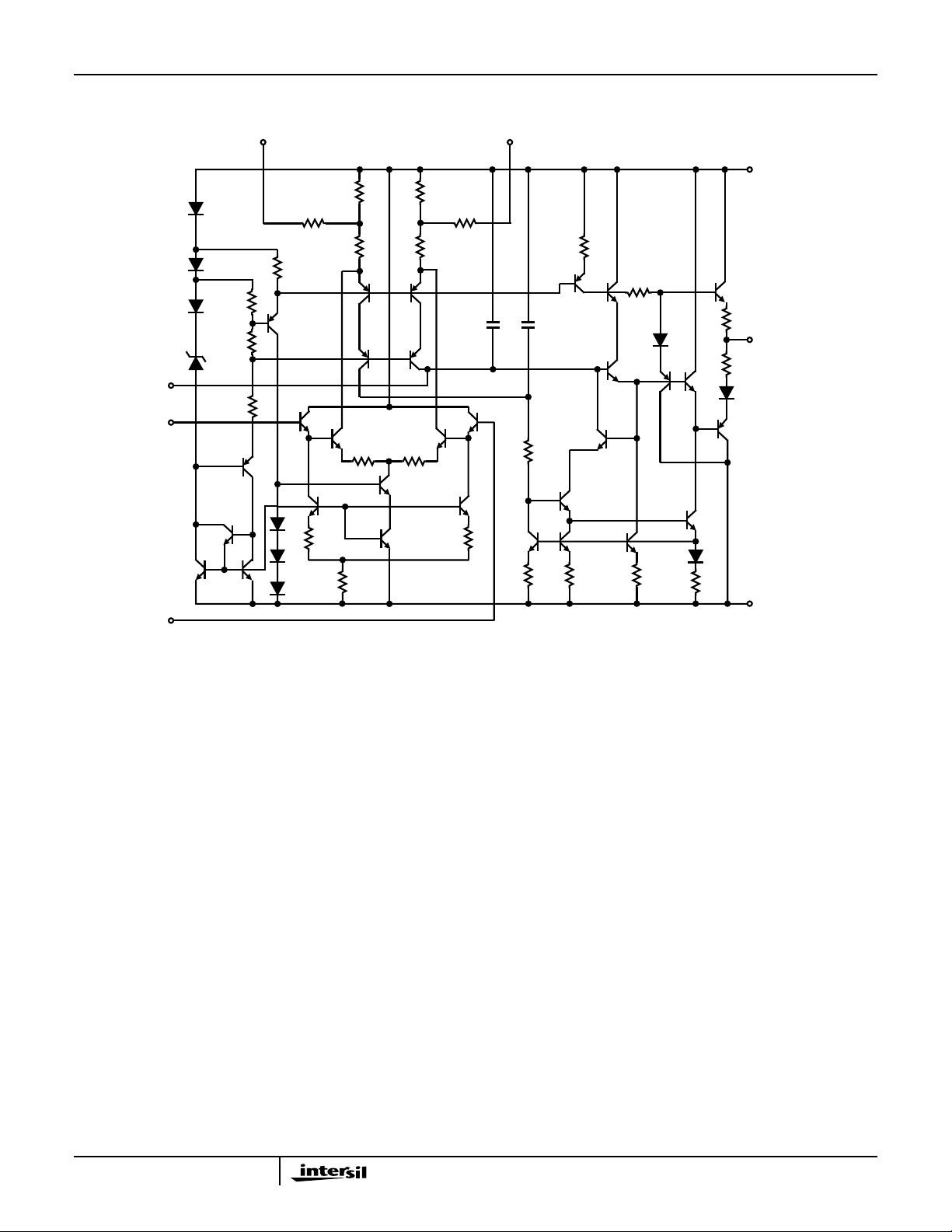
Schematic
COMP
+ INPUT
HA-2505
R
200
BAL
V+
8
R
11
2K
R
12
1.1K
Q
10
Q
C
2
Q
26
C
1
10pF
Q
13
R
19
6.3K
Q
25
Q
23
Q
24
R
R
18
1.48K
1.48K
11
Q
14
Q
Q
12
15
Q
22
17
R
16
1.48K
Q
16
R
13
30
OUTPUT
R
14
30
Q
17
Q
18
Q
19
Q
20
Q
21
R
15
740
V-
BAL
R
R
6
R
Q
1
Q
2
R
11.13K
Q
34
2K
R
960
R
Q
2
3
4
Q
35
32
Q
3
Q
4
Q
33
5
200
R
1
4K
Q
5
Q
37
Q
38
800
R
Q
29
Q
30
R
23
3.3K
Q
31
Q
36
R
1.12K
200
R
7
1.8K
Q6Q
Q7Q
25
22
200
R
1.8K
Q
Q
9
10
8
10.6pF
9
Q
40
Q
39
800
R
26
28
R
27
20
3.3K
- INPUT
2

HA-2505
Absolute Maximum Ratings Thermal Information
Supply Voltage Between V+ and V- Terminals. . . . . . . . . . . . . . 40V
Differential Input Voltage . . . . . . . . . . . . . . . . . . . . . . . . . . . . . . 15V
Peak Output Current . . . . . . . . . . . . . . . . . . . . . . . . . . . . . . . . 50mA
Operating Conditions
Temperature Range
HA-2505-5 . . . . . . . . . . . . . . . . . . . . . . . . . . . . . . . . 0oC to 75oC
CAUTION: Stresses above those listed in “Absolute Maximum Ratings” may cause permanent damage to the device. This is a stress only rating and operation of the
device at these or any other conditions above those indicated in the operational sections of this specification is not implied.
NOTE:
1. θJA is measured with the component mounted on an evaluation PC board in free air.
Thermal Resistance (Typical, Note 1) θJA (oC/W)
PDIP Package. . . . . . . . . . . . . . . . . . . . . . . . . . . . . 96
Maximum Junction Temperature (Plastic Package) . . . . . . . . 150oC
Maximum Storage Temperature Range . . . . . . . . . -65oC to 150oC
Maximum Lead Temperature (Soldering 10s). . . . . . . . . . . . 300oC
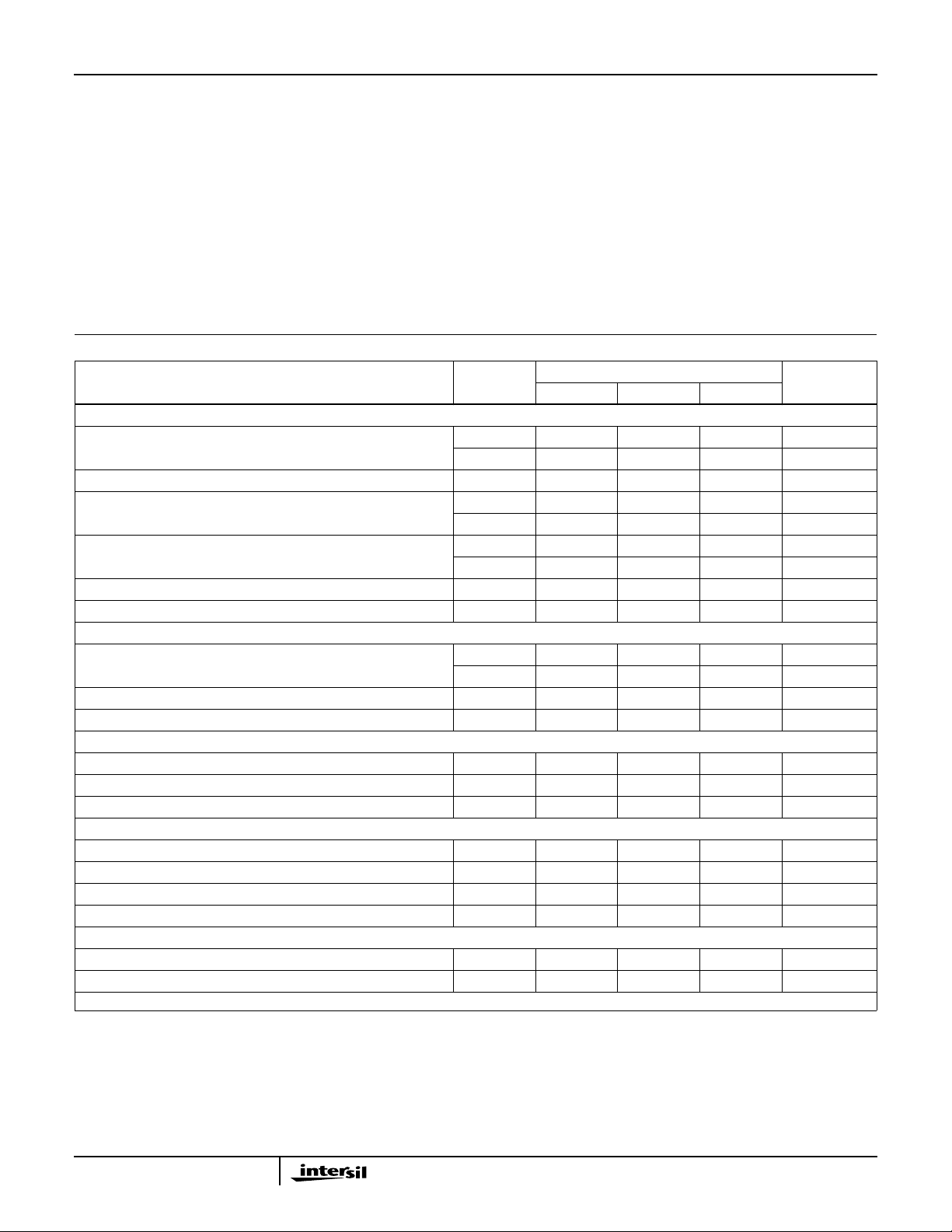
Electrical Specifications V
PARAMETER
INPUT CHARACTERISTICS
Offset Voltage 25 - 4 8 mV
Offset Voltage Average Drift Full - 20 - µV/oC
Bias Current 25 - 125 250 nA
Offset Current 25 - 20 50 nA
Input Resistance (Note 2) 25 20 50 - MΩ
Common Mode Range Full ±10 - - V
TRANSFER CHARACTERISTICS
Large Signal Voltage Gain (Notes 3, 6) 25 15 25 - kV/V
Common Mode Rejection Ratio (Note 4) Full 74 90 - dB
Gain Bandwidth Product (Note 5) 25 - 12 - MHz
OUTPUT CHARACTERISTICS
Output Voltage Swing (Note 3) Full ±10 ±12 - V
Output Current (Note 6) 25 ±10 ±20 - mA
Full Power Bandwidth (Notes 6, 11) 25 300 500 - kHz
TRANSIENT RESPONSE
Rise Time (Notes 3, 7, 8, 9) 25 - 25 50 ns
Overshoot (Notes 3, 7, 8, 9) 25 - 25 50 %
Slew Rate (Notes 3, 7, 9, 12) 25 ±20 ±30 - V/µs
Settling Time to 0.1% (Notes 3, 7, 9, 12) 25 - 0.33 - µs
POWER SUPPLY CHARACTERISTICS
Supply Current 25 - 4 6 mA
PSRR (Note 10) Full 74 90 - dB
NOTES:
2. This parameter value is based on design calculations.
3. RL = 2kΩ.
4. VCM = ±10V.
5. AV > 10.
6. VO = ±10V.
7. CL = 50pF.
= ±15V
S
TEMP
(oC)
Full - - 10 mV
Full - - 500 nA
Full - - 100 nA
Full 10 - - kV/V
8. VO = ±200mV.
9. See Transient Response Test Circuits and Waveforms.
10. ∆V = ±5V.
11. Full Power Bandwidth guaranteed based on slew rate measurement
using: FPBW = Slew Rate/2πV
12. V
OUT
= ±5V.
HA-2505-5
PEAK
UNITSMIN TYP MAX
.
3
 Loading...