

查询EL9200供应商
®
EL9200, EL9201, EL9202
Data Sheet April 7, 2005
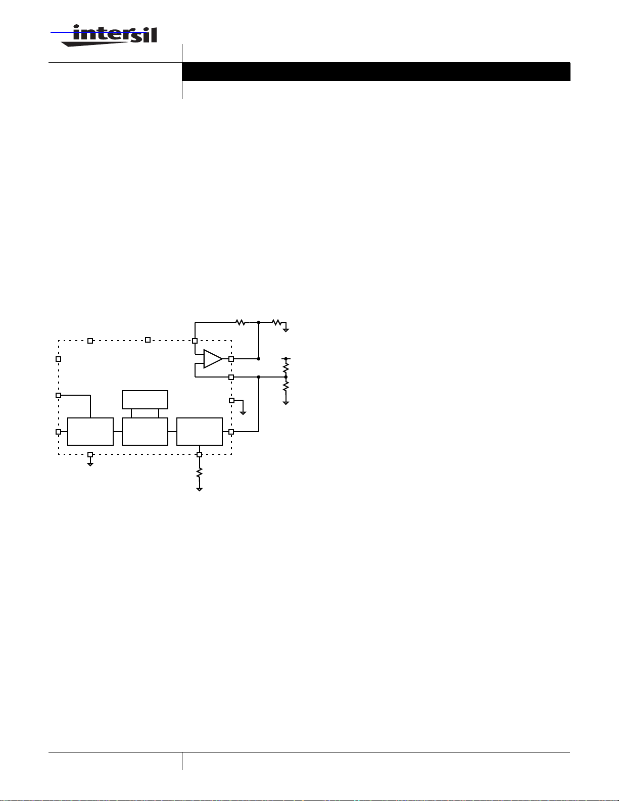
Programmable V
The EL9200, EL9201, and EL9202 represent programmable
V
amplifiers for use in TFT-LCD displays. Featuring 1,
COM
2, and 4 channels of V
device features just a single programmable current source
for adding offset to one V
programmable using a single wire interface to one of 128
levels. The value is stored on an internal EEPROM memory.
The EL9200 is available in the 12-pin DFN package and the
EL9201 and EL9202 are available in 24-pin QFN packages.
All are specified for operation over the -40°C to +85°C
temperature range.
COM
amplification, respectively, each
COM
output. This current source is
COM
Typical Block Diagram
R
F
A
VDD
V
SD
CE
VS+
EEPROM
INN
V
-
+
OUT
INP
GND
FN7438.0
Features
• 128 step adjustable sink current
• EEPROM memory
• 2-pin adjustment and disable
• Single, dual or quad amplifiers
- 44MHz bandwidth
- 80V/µs slew rate
- 60mA continuous output
- 180mA peak output
• Up to 18V operation
• 2.6V to 3.6V logic control
• Pb-free available (RoHS compliant)
R
G
A
VDD
R
1
R
2
Applications
•TFT-LCD V
-LCD-TVs
- LCD monitors
COM
supplies for
CTL
CONTROL
GND SET
UP/DOWN
COUNTER
ANALOG
POT
R
SET
I
OUT
1
CAUTION: These devices are sensitive to electrostatic discharge; follow proper IC Handling Procedures.
1-888-INTERSIL or 321-724-7143
| Intersil (and design) is a registered trademark of Intersil Americas Inc.
All other trademarks mentioned are the property of their respective owners.
Copyright © Intersil Americas Inc. 2005. All Rights Reserved.
Pinouts
1
VINA-
EL9200
(12-PIN DFN)
TOP VIEW
EL9200, EL9201, EL9202
EL9201
(24-PIN QFN)
TOP VIEW
NC
GND
NC
VINA+
VINA-
24
23
22
21
20
12
VS+
NC
1
19
NC
VOUTA
1
EL9202
(24-PIN QFN)
TOP VIEW
VINA-
VINA+
24
23
VS+
VINB+
VINB-
22
21
20
19
VOUTB
GND
VINA+
IOUT
AVD D
GND
2
3
4
5
6
THERMAL
PAD
11
10
9
8
7
VOUTA
SET
CE
CTL
VSD
NC
VINB+
IOUT
NC
AVD D
GND
11
VSD
18
VOUTA
17
VS+
16
VOUTB
15
VINB-
14
SET
13
CE
12
CTL
VOUTD
VIND-
NC
VIND+
AVD D
CTL
2
3
8
CE
THERMAL
PAD
9
10
NC
SET
4
5
6
7
11
IOUT
12
NC
18
17
16
15
14
13
VOUTC
VINC-
NC
VINC+
GND
AVD D
2
3
8
NC
THERMAL
PAD
9
10
NC
NC
4
5
6
7
Ordering Information
PART NUMBER PACKAGE
EL9200IL 12-Pin DFN - MDP0047 EL9201ILZ
EL9200IL-T7 12-Pin DFN 7” MDP0047 EL9201ILZ-T7
EL9200IL-T13 12-Pin DFN 13” MDP0047 EL9201ILZ-T13
EL9200ILZ
(See Note)
EL9200ILZ-T7
(See Note)
EL9200ILZ-T13
(See Note)
12-Pin DFN
(Pb-Free)
12-Pin DFN
(Pb-Free)
12-Pin DFN
(Pb-Free)
EL9201IL 24-Pin QFN - MDP0046 EL9202ILZ
EL9201IL-T7 24-Pin QFN 7” MDP0046 EL9202ILZ-T7
EL9201IL-T13 24-Pin QFN 13” MDP0046 EL9202ILZ-T13
REEL PKG. DWG. # PART NUMBER PACKAGE
24-Pin QFN
(See Note)
(Pb-Free)
24-Pin QFN
(See Note)
(Pb-Free)
24-Pin QFN
(See Note)
(Pb-Free)
- MDP0047 EL9202IL 24-Pin QFN - MDP0046
7” MDP0047 EL9202IL-T7 24-Pin QFN 7” MDP0046
13” MDP0047 EL9202IL-T13 24-Pin QFN 13” MDP0046
24-Pin QFN
(See Note)
(Pb-Free)
24-Pin QFN
(See Note)
(Pb-Free)
24-Pin QFN
(See Note)
(Pb-Free)
NOTE: Intersil Pb-free products employ special Pb-free material sets; molding compounds/die attach materials and 100% matte tin plate termination
finish, which are RoHS compliant and compatible with both SnPb and Pb-free soldering operations. Intersil Pb-free products are MSL classified at
Pb-free peak reflow temperatures that meet or exceed the Pb-free requirements of IPC/JEDEC J STD-020.
TAPE &
TAPE &
REEL PKG. DWG. #
- MDP0046
7” MDP0046
13” MDP0046
- MDP0046
7” MDP0046
13” MDP0046
2
FN7438.0
April 7, 2005
EL9200, EL9201, EL9202
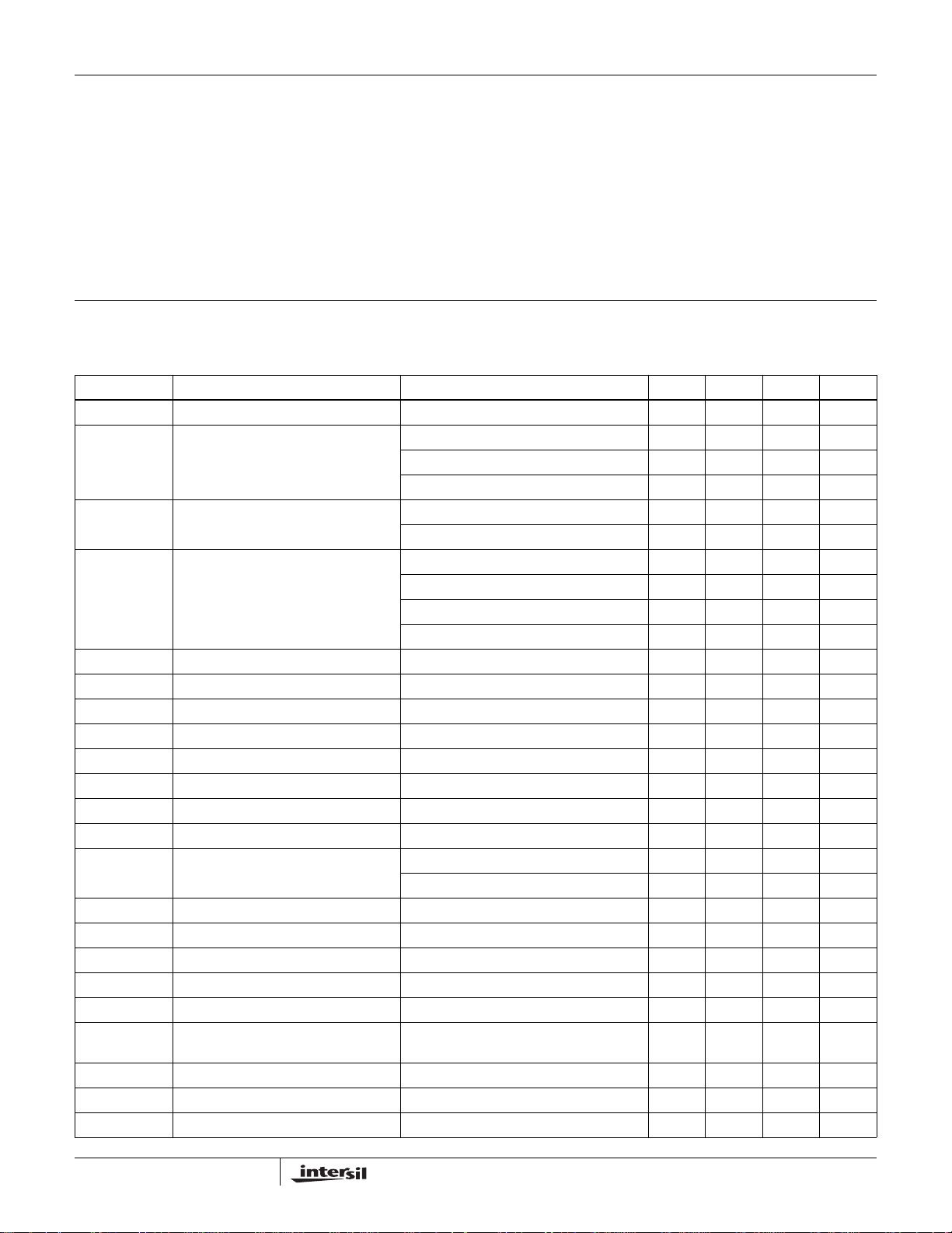
Absolute Maximum Ratings (T
V
+ Supply Voltage between VS+ and GND . . . . . . . . . . . . . .18V
S
Supply Voltage between V
Maximum Continuous Output Current . . . . . . . . . . . . . . . . . . . 65mA
Input Voltages to GND
SET, CE . . . . . . . . . . . . . . . . . . . . . . . . . . . . . . . . . . . -0.3V to +4V
CTL. . . . . . . . . . . . . . . . . . . . . . . . . . . . . . . . . . . . . . -0.3V to +16V
and GND . . . . . . . . . . . . . . . . . . . .4V
SD
= 25°C)
A
A
. . . . . . . . . . . . . . . . . . . . . . . . . . . . . . . . . . . . . . -0.3V to +20V
VDD
ESD Rating - HBM for Device . . . . . . . . . . . . . . . . . . . . . . . . . . . 2kV
Ambient Operating Temperature . . . . . . . . . . . . . . . . -40°C to +85°C
Maximum Die Temperature . . . . . . . . . . . . . . . . . . . . . . . . . . +150°C
Storage Temperature . . . . . . . . . . . . . . . . . . . . . . . . -65°C to +150°C
Maximum Lead Temperature (Soldering 10s) . . . . . . . . . . . . +300°C
Output Voltages to GND
OUT . . . . . . . . . . . . . . . . . . . . . . . . . . . . . . . . . . . . . -0.3V to +20V
CAUTION: Stresses above those listed in “Absolute Maximum Ratings” may cause permanent damage to the device. This is a stress only rating and operation of the
device at these or any other conditions above those indicated in the operational sections of this specification is not implied.
IMPORTANT NOTE: All parameters having Min/Max specifications are guaranteed. Typical values are for information purposes only. Unless otherwise noted, all tests
are at the specified temperature and are pulsed tests, therefore: T
Electrical Specifications V
= 3V, VS+ = 15V, A
SD
= TC = T
J
VDD
A
= 15V, R
= 24.9kΩ, and TA = 25°C unless otherwise specified
SET
PARAMETER DESCRIPTION CONDITION MIN TYP MAX UNIT
V
S+
I
S+
Supply Voltage 4.5 16.5 V
Quiescent Current EL9200 3.8 4.8 mA
EL9201 7.6 9.6 mA
EL9202 10.5 16 mA
V
SD
Logic Supply Voltage For programming 3 3.6 V
For operation 2.6 3.6 V
I
SD
Quiescent Logic Current CE = 3.6V 50 µA
CE = GND 25 µA
Program (charge pump current) (Note 1) 23 mA
Read (Note 1) 3 mA
I
ADD
CTL
CTL
CTL
CTL
CTL
CTL
CTL
IH
IL
IHRPW
ILRPW
IHMPW
ILMPW
MTC
Supply Current Note 2 25 µA
CTL High Voltage 2.6V < VSD < 3.6V 0.7*V
CTL Low Voltage 2.6V < VSD < 3.6V 0.2*V
SD
SD
0.8*V
0.3*V
SD
SD
CTL High Rejected Pulse Width 20 µs
CTL Low Rejected Pulse Width 20 µs
CTL High Minimum Pulse Width 200 µs
CTL Low Minimum Pulse Width 200 µs
CTL Minimum Time Between Counts 10 µs
V
V
ICTL CTL Input Current CTL = GND 10 µA
CTL
CE
CE
CE
CTL
CTL
P
T
EE
SET
CAP
IL
IH
ST
PROM
PT
WC
DN
CTL = V
SD
CTL Input Capacitance 10 pF
CE Input Low Voltage 2.6V < VSD < 3.6V 0.4 V
CE Input High Voltage 2.6V < VSD < 3.6V 1.6 V
CE Minimum Start Up Time (Note 1) 1 ms
CTL EEPROM Program Voltage 2.6V < VSD < 3.6V (Note 2) 4.9 15.75 V
CTL EEPROM Programming Signal
> 4.9V 200 µs
Time
Programming Time 100 ms
EE Write Cycles Guaranteed by design 1000 cycles
SET Differential Nonlinearity Monotonic over-temperature ±1LSB
10 µA
3
FN7438.0
April 7, 2005
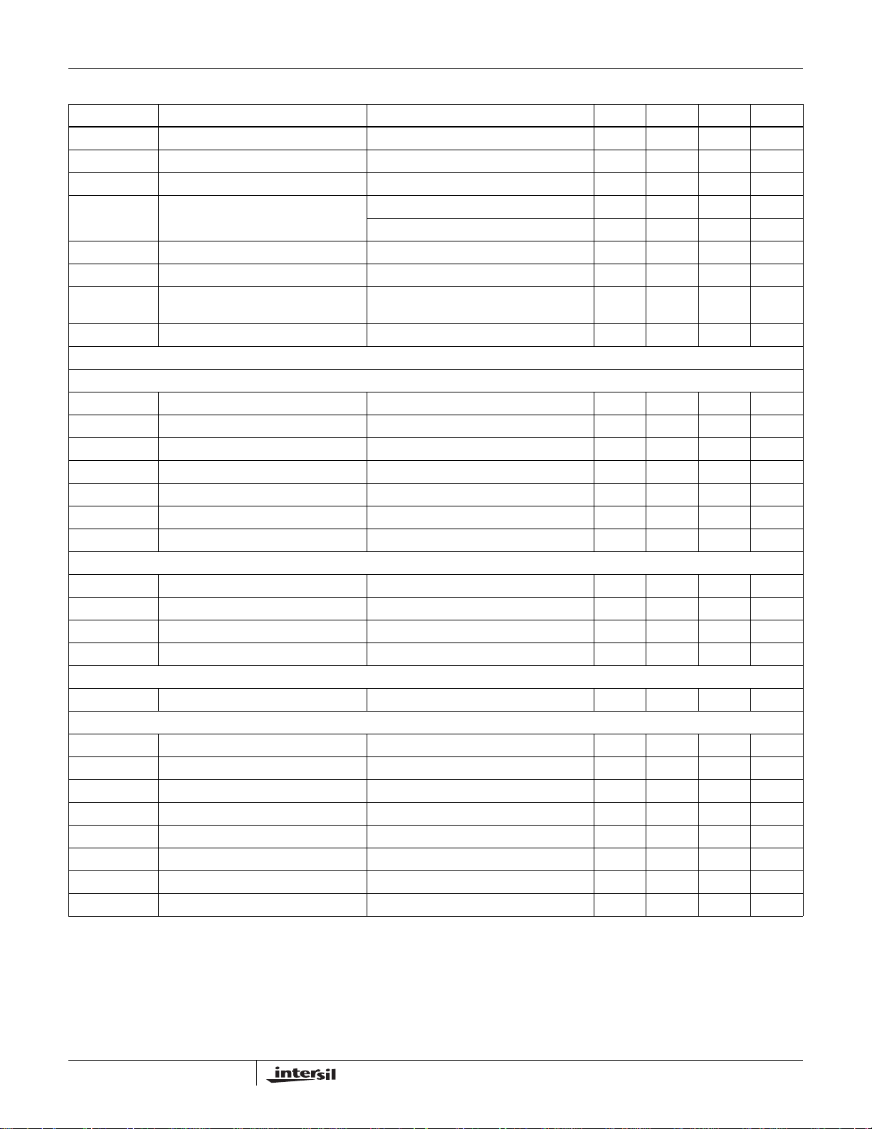
EL9200, EL9201, EL9202
Electrical Specifications V
= 3V, VS+ = 15V, A
SD
VDD
= 15V, R
= 24.9kΩ, and TA = 25°C unless otherwise specified
SET
PARAMETER DESCRIPTION CONDITION MIN TYP MAX UNIT
SET
ZSE
SET
FSE
I
SET
SET
ER
A
to SET A
VDD
OUT
ST
V
OUT
SET Zero-Scale Error Note 3 ±2LSB
SET Full-Scale Error Note 3 ±8LSB
SET Current Through R
SET External Resistance To GND, A
To GND, A
to SET Voltage Attenuation 1:20 V/V
VDD
(Note 1) 120 µA
SET
= 20V (Note 1) 10 200 kΩ
VDD
= 4.5V (Note 1) 2.25 45 kΩ
VDD
OUT Settling Time To ±0.5 LSB error band (Note 1) 20 µs
OUT Voltage Range (Note 1) V
SET
+
13 V
0.5V
OUT
VD
OUT Voltage Drift (Note 1) 10 mV
AMPLIFIER CHARACTERISTICS
INPUT CHARACTERISTICS
V
OS
TCV
OS
I
B
R
IN
C
IN
CMRR Common-Mode Rejection Ratio For V
A
VOL
Input Offset Voltage VCM = 0V 3 15 mV
Average Offset Voltage Drift (Note 1) 7 µV/°C
Input Bias Current VCM = 0V 2 60 nA
Input Impedance 1GΩ
Input Capacitance 2pF
from -5.5V to +5.5V 50 70 dB
IN
Open-Loop Gain -4.5V ≤ V
≤ +4.5V 60 70 dB
OUT
OUTPUT CHARACTERISTICS
V
V
I
SC
I
OUT
OL
OH
Output Swing Low RL = 1.5kΩ to 0 0.09 0.15 V
Output Swing High 14.85 14.9 V
Short-Circuit Current ±150 ±180 mA
Output Current ±65 mA
POWER SUPPLY PERFORMANCE
PSRR Power Supply Rejection Ratio V
is moved from 4.5V to 15.5V 55 80 dB
S+
DYNAMIC PERFORMANCE
SR Slew Rate (Note 4) -4.0V ≤ V
t
S
Settling to +0.1% (AV = +1) (AV = +1), V
≤ 4.0V, 20% to 80% 60 80 V/µs
OUT
= 2V step 80 ns
OUT
BW -3dB Bandwidth 44 MHz
GBWP Gain-Bandwidth Product 32 MHz
PM Phase Margin 50 °
CS Channel Separation f = 5MHz (EL9201 & EL9202 only) 110 dB
d
G
d
P
Differential Gain (Note 5) RF = RG = 1kΩ and V
Differential Phase (Note 5) RF = RG = 1kΩ and V
= 1.4V 0.17 %
OUT
= 1.4V 0.24 °
OUT
NOTES:
1. Simulated and determined via design and not directly tested
2. Tested at A
VDD
= 20V
3. Wafer sort only
4. NTSC signal generator used
4
FN7438.0
April 7, 2005
EL9200, EL9201, EL9202
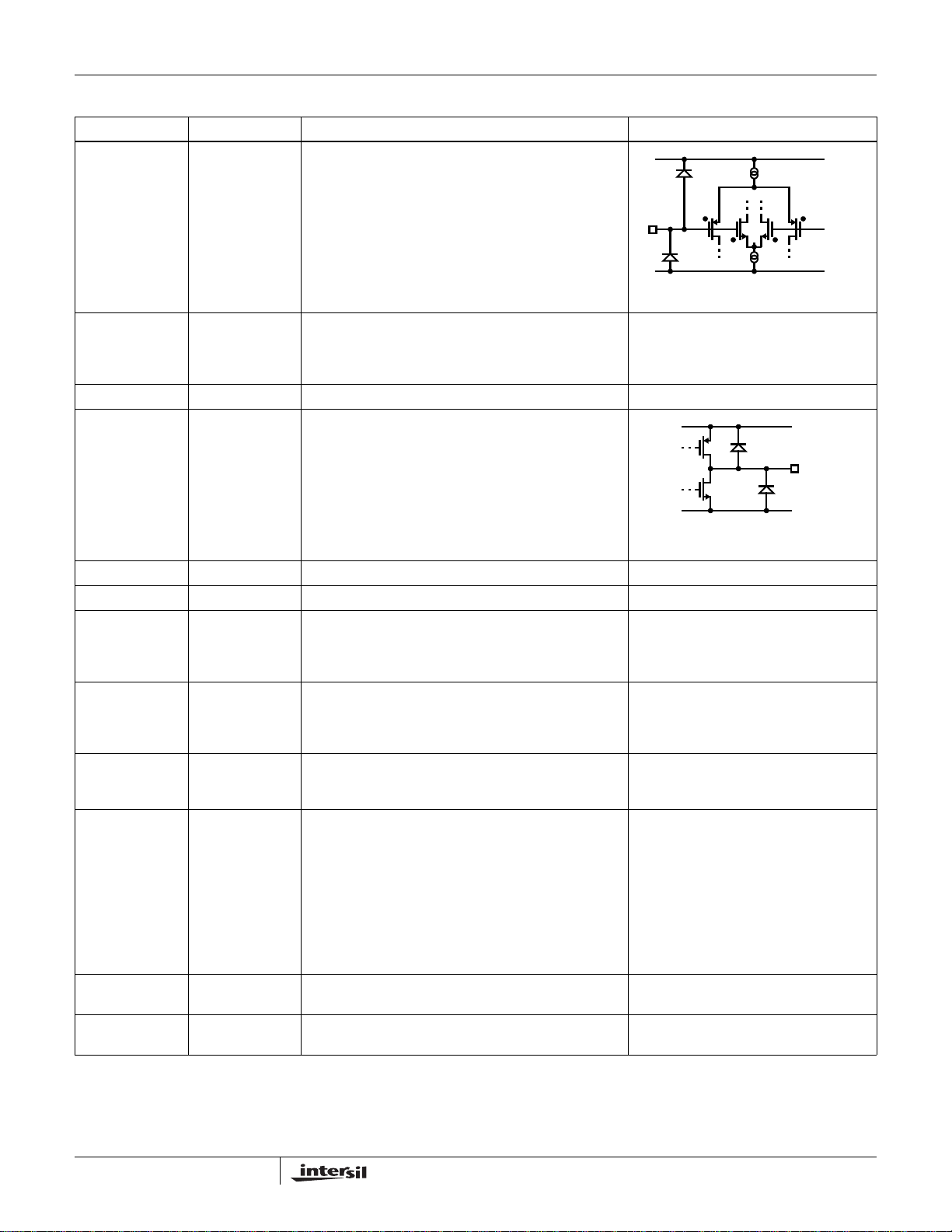
Pin Descriptions
PIN IN/OUT DESCRIPTION EQUIVALENT CIRCUIT
VINX- Input Amplifier X inverting input, where:
VINX+ Input Amplifier X non-inverting input, where:
VS+ Supply Op amp supply; bypass to GND with 0.1µF capacitor
VOUTX Output Amplifier X output, where:
X = A for EL9200
X = A, B for EL9201
X = A, B, C, D for EL9202
Reference Circuit 1
X = A for EL9200
X = A, B for EL9201
X = A, B, C, D for EL9202
X = A for EL9200
X = A, B for EL9201
X = A, B, C, D for EL9202
CIRCUIT 1
V
S+
GND
V
S+
NC - No connect; not internally connected
GND Supply Ground connection
IOUT Output Adjustable sink current output pin; the current sinks into the
OUT pin is equal to the DAC setting times the maximum
adjustable sink current divided by 128; see SET pin function
description for the maxim adjustable sink current setting
SET Output Maximum sink current adjustment point; connect a resistor
from SET to GND to set the maximum adjustable sink
current of the OUT pin; the maximum adjustable sink
current is equal to (A
/20) divided by R
VDD
SET
CE Input Counter enable pin; connect CE to VDD to enable counting
of the internal counter; connect CE to GND to inhibit
counting
CTL Input Internal counter up/down control and internal EEPROM
programming control input; if CE is high, a mid-to-low
transition increments the 7-bit counter, raising the DAC
setting, increasing the OUT sink current, and lowering the
divider voltage at OUT; a mid-to-high transition decrements
the 7-bit counter, lowering the DAC setting, decreasing the
OUT sink current, and increasing the divider voltage at
OUT; applying 4.9V and above with appropriately arranged
timing will overwrite EEPROM with the contents in the 7-bit
counter; see EEPROM Programming section for details
AVDD Supply analog voltage supply; bypass to GND with 0.1µF
capacitor
VSD Supply System power supply input; bypass to GND with 0.1µF
capacitor
GND
GND
CIRCUIT 2
5
FN7438.0
April 7, 2005

EL9200, EL9201, EL9202
Amplifier Typical Performance Curves
QUANTITY (AMPLIFIERS)
500
400
300
200
100
0
VS=5V
=25°C
T
A
-8-6-4
-12
-10
INPUT OFFSET VOLTAGE (mV)
-2
0
2
TYPICAL
PRODUCTION
DISTRIBUTION
4
6
8
10
12
0.008
VS=5V
0.004
0
-0.004
-0.008
INPUT BIAS CURRENT (µA)
-0.012
-50 -10 30 70 110 150
TEMPERATURE (°C)
FIGURE 1. INPUT OFFSET VOLTAGE DISTRIBUTION FIGURE 2. INPUT BIAS CURRENT vs TEMPERATURE
25
VS=5V TYPICAL
20
15
10
PRODUCTION
DISTRIBUTION
4.96
4.94
4.92
4.9
VS=5V
I
OUT
=5mA
5
QUANTITY (AMPLIFIERS)
0
1
3
5
7
9
11
13
15
17
19
21
INPUT OFFSET VOLTAGE DRIFT, TCV
OS
(µV/°C)
4.88
OUTPUT HIGH VOLTAGE (V)
4.86
-50 -10 30 70 110 150
TEMPERATURE (°C)
FIGURE 3. INPUT OFFSET VOLTAGE DRIFT FIGURE 4. OUTPUT HIGH VOLTAGE vs TEMPERATURE
2
1.5
1
0.5
0
INPUT OFFSET VOLTAGE (mV)
-0.5
-50 -10 30 70 110 150
TEMPERATURE (°C)
-4.85
VS=5V
=5mA
I
OUT
-4.87
-4.89
-4.91
-4.93
OUTPUT LOW VOLTAGE (V)
-4.95
-50 -10 30 70 110 150
TEMPERATURE (°C)
FIGURE 5. INPUT OFFSET VOLTAGE vs TEMPERATURE FIGURE 6. OUTPUT LOW VOLTAGE vs TEMPERATURE
6
FN7438.0
April 7, 2005

EL9200, EL9201, EL9202
Amplifier Typical Performance Curves
75
70
65
OPEN-LOOP GAIN (dB)
60
-50 -10 30 70 110 150
TEMPERATURE (°C)
VS=±5V
=1kΩ
R
L
78
VS=±V
77
76
75
74
SLEW RATE (V/µs)
73
72
-50 -10 30 70 110 150
TEMPERATURE (°C)
FIGURE 7. OPEN-LOOP GAIN vs TEMPERATURE FIGURE 8. SLEW RATE vs TEMPERATURE
0
-0.02
-0.04
-0.06
-0.08
-0.1
-0.12
-0.14
DIFFERENTIAL GAIN (%)
-0.16
-0.18
0 100 200
IRE
VS=5V
=2
A
V
=1kΩ
R
L
0.3
0.25
0.2
0.15
0.1
DIFFERENTIAL PHASE (°)
0.05
0
0 100 200
IRE
FIGURE 9. DIFFERENTIAL GAIN FIGURE 10. DIFFERENTIAL PHASE
-30
VS=5V
=2
A
V
-40
R
=1kΩ
L
FREQ=1MHz
-50
-60
-70
DISTORTION (dB)
-80
-90
0810
246
FIGURE 11. HARMONIC DISTORTION vs V
V
OP-P
2nd HD
3rd HD
(V)
OP-P
80
60
40
20
GAIN (dB)
0
-20
1K 10M 100M
10K 100K 1M
FREQUENCY (Hz)
GAIN
PHASE
FIGURE 12. OPEN LOOP GAIN AND PHASE
250
190
130
70
10
-50
PHASE (°)
7
FN7438.0
April 7, 2005

EL9200, EL9201, EL9202
Amplifier Typical Performance Curves
5
VS=5V
=1
A
V
=0pF
C
LOAD
3
1
-1
-3
MAGNITUDE (NORMALIZED) (dB)
-5
100K 100M
1M 10M
FREQUENCY (Hz)
150Ω
1kΩ
560Ω
FIGURE 13. FREQUENCY RESPONSE FOR VARIOUS R
400
350
300
250
200
150
100
OUTPUT IMPEDANCE (Ω)
50
0
10K 100M
100K 10M
1M
FREQUENCY (Hz)
25
15
5
-5
-15
VS=5V
A
MAGNITUDE (NORMALIZED) (dB)
L
FIGURE 14. FREQUENCY RESPONSE FOR VARIOUS C
)
P-P
MAXIMUM OUTPUT SWING (V
V
R
-25
100K 100M
12
10
8
6
4
VS=5V
A
V
2
R
DISTORTION <1%
0
10K 100M
1000pF
=1
=1kΩ
L
1M 10M
FREQUENCY (Hz)
=1
=1kΩ
L
100K 10M
FREQUENCY (Hz)
100pF
47pF
10pF
L
1M
FIGURE 15. CLOSED LOOP OUTPUT IMPEDANCE FIGURE 16. MAXIMUM OUTPUT SWING vs FREQUENCY
-15
-25
-35
-45
CMRR (dB)
-55
-65
1K 100M
10K
100K 10M
FREQUENCY (Hz)
1M
-80
-60
-40
PSRR (dB)
-20
0
100 10M
PSRR+ VS=5V
PSRR-
10K 1M100K1K
FREQUENCY (Hz)
T
A
=25°C
FIGURE 17. CMRR FIGURE 18. PSRR
8
FN7438.0
April 7, 2005

EL9200, EL9201, EL9202
Amplifier Typical Performance Curves
1K
100
10
VOLTAGE NOISE (nV/√Hz)
1
100 100M
10K 1M100K1K
FREQUENCY (Hz)
10M
-60
DUAL MEASURED CH A TO B
QUAD MEASURED CH A TO D OR B TO C
OTHER COMBINATIONS YIELD
-80
IMPROVED REJECTION
-100
-120
XTALK (dB)
VS=5V
-140
-160
=1kΩ
R
L
=1
A
V
=110mV
V
IN
1K 30M
RMS
100K 10M1M10K
FREQUENCY (Hz)
FIGURE 19. INPUT VOLTAGE NOISE SPECTRAL DENSITY FIGURE 20. CHANNEL SEPARATION
100
VS=5V
=1
A
V
=1kΩ
R
L
80
=50mV
V
IN
=25°C
T
A
60
40
OVERSHOOT (%)
20
STEP SIZE (V)
-1
-3
5
3
1
VS=5V
=1
A
V
=1kΩ
R
L
0.1%
0.1%
0
10 1K
LOAD CAPACITANCE (pF)
100
FIGURE 21. SMALL-SIGNAL OVERSHOOT vs LOAD
-5
55 105
75 9565
SETTLING TIME (ns)
85
FIGURE 22. SETTLING TIME vs STEP SIZE
CAPACITANCE
1V STEP
50ns/DIV
VS=±5V
T
=25°C
A
=1
A
V
=1kΩ
R
L
100mV STEP
50ns/DIV
VS=±5V
T
A
A
V
R
L
FIGURE 23. LARGE SIGNAL TRANSIENT RESPONSE FIGURE 24. SMALL SIGNAL TRANSIENT RESPONSE
=25°C
=1
=1kΩ
9
FN7438.0
April 7, 2005

EL9200, EL9201, EL9202
Amplifier Typical Performance Curves
JEDEC JESD51-7 HIGH EFFECTIVE THERMAL
CONDUCTIVITY TEST BOARD - QFN EXPOSED
DIEPAD SOLDERED TO PCB PER JESD51-5
4.5
4
3.378W
3.5
3
2.5
2
1.5
1
POWER DISSIPATION (W)
0.5
0
0 150
FIGURE 25. PACKAGE POWER DISSIPATION vs AMBIENT
TEMPERATURE
Q
F
θ
N
J
2
A
4
=
3
7
°
C
/
W
25 10050 12585
AMBIENT TEMPERATURE (°C)
75
JEDEC JESD51-3 LOW EFFECTIVE THERMAL
CONDUCTIVITY TEST BOARD
1.2
1
893mW
0.8
0.6
0.4
POWER DISSIPATION (W)
0.2
0
0 150
Q
F
θ
N
J
2
A
=
4
1
4
0
°
C
/
W
25 10050 12585
AMBIENT TEMPERATURE (°C)
75
FIGURE 26. PACKAGE POWER DISSIPATION vs AMBIENT
TEMPERATURE
Application Information
This device provides the ability to reduce the flicker of an
LCD panel by adjustment of the V
production test and alignment. A 128-step resolution is
provided under digital control which adjusts the sink current
of the output. The output is connected to an external voltage
divider, so that the device will have the capability to reduce
the voltage on the output by increasing the output sink
current.
The adjustment of the output and the programming of the
non-volatile memory are provided on one pin while the
counter enable (CE) is provided on a separate pin. The
output is adjusted via the CTL pin either by counting up with
a mid to low transition or by counting down with a mid to high
transition. Once the minimum or maximum value is reached
on the 128 steps, the device will not overflow or underflow
beyond that minimum or maximum value. An increment of
the counter will increase the output sink current which will
lower the voltage on the external voltage divider. A
decrement of the counter will decrease the output sink
current, which will raise the voltage on the external voltage
divider.
Once the desired output level is obtained, the part can store
it's setting using the non-volatile memory in the device. See
the non-volatile programming section for detailed
information.
NOTE: Once the desired output level is stored in the EEPROM, the
CE pin must go low to preserve the stored value.
voltage during
COM
Adjustable Sink Current Output
The device provides an output sink current which lowers the
voltage on the external voltage divider. The equations that
control the output are given below:
R
+
×=
2
2
---------------------------
20 R
A
VDD
()
SET
Setting
---------------------
V
1
AVDD
128
R
---------------------------
×–
20 R
()
1
SET
Setting
OUT
OUT
---------------------
128
---------------------
=
R1R
I
V
NOTE: Where setting is an integer between 1 and 128.
7-Bit Up/Down Counter
The counter sets the level to the digital potentiometer and is
connected to the non-volatile memory. When the part is
programmed, the counter setting is loaded into the nonvolatile memory. This value will be loaded from the nonvolatile memory into the counter during power-on. The
counter will not exceed its maximum level and will hold that
value during subsequent increment requests on the CTL pin.
The counter will not exceed its minimum level and will hold
that value during subsequent decrement requests on the
CTL pin.
CTL Pin
CTL should have a noise filter to reduce bouncing or noise
on the input that could cause unwanted counting when the
CE pin is high. The board should have an additional ESD
protection circuit, with a series 1kΩ resistor and a shunt
0.01µF capacitor connected on the CTL pin.
10
In order to increment the setting, pulse CTL low for more
than 200µs. The output sink current increases and lowers
the V
lever by one least-significant bit (LSB). On the
COM
other hand, to decrement the setting, pulse CTL high for
FN7438.0
April 7, 2005

EL9200, EL9201, EL9202
more than 200µs. The output sink current will decrease and
the V
level will increase by one LSB.
COM
To avoid unintentional adjustment, the EL9200, EL9201, and
EL9202 guarantees to reject CTL pulses shorter than 20µs.
Since the internal comparators come up in an unknown
state, the very first CTL pulse is ignored to avoid the
possibility of a false pulse.
See Figure 27 for the timing information.
TABLE 1. TRUTH TABLE
INPUT OUTPUT
CTL CE V
Mid to Hi Hi V
Mid to Lo Hi V
XLoV
> 4.9V X V
X X 0 to V
DD
DD
DD
DD
DD
DD
SET I
CC
Decrement Normal X
Increment Normal X
No Change Lower X
No Change Increased Program
Read Increased Read
MEMORY
NOTE: CE should be disabled (pulled low) before powering down the device to assure that the glitches and transients will not cause unwanted
EEPROM overwriting.
CTL
CTL HIGH
V
DD
CTL
MTC
/2
CTL
IHRPW
CE
COUNTER
OUTPUT
V
COM
CTL LOW
CTL
IHMPW
78 79 7A 7B 7AUNDEF
FIGURE 27. V
CTL
ADJUSTMENT
COM
ILMPW
CTL
ILRPW
11
FN7438.0
April 7, 2005

EL9200, EL9201, EL9202
Non-Volatile Memory (EEPROM)
Programming
When the CTL pin exceeds 4.9V, the non-volatile
programming cycle will be activated. The CTL signal needs
to remain above 4.9V for more than 200µs. The level and
timing needed to program the non-volatile memory is given
below. It then takes a maximum of 100ms for the
programming to be completed inside the device (see P
specification in Electrical Specification Table).
CTL VOLTAGE
4.9V
CTL
PT
FIGURE 28. EEPROM PROGRAMMING
Amplifiers’ Operating Voltage, Input, and Output
The amplifiers are specified with a single nominal supply
voltage from 5V to 15V or a split supply with its total range
from 5V to 15V. Correct operation is guaranteed for a supply
range of 4.5V to 16.5V. Most amplifier specifications are
stable over both the full supply range and operating
temperatures of -40°C to +85°C. Parameter variations with
operating voltage and/or temperature are shown in the
typical performance curves.
The input common-mode voltage range of the amplifiers
extends 500mV beyond the supply rails. The output swings
of the those typically extend to within 100mV of positive and
negative supply rails with load currents of 5mA. Decreasing
load currents will extend the output voltage range even
closer to the supply rails. Figure 27 shows the input and
output waveforms for the device in the unity-gain
configuration. Operation is from 5V supply with a 1kΩ load
connected to GND. The input is a 10V
output voltage is approximately 9.8V
5V
5V
10µs
sinusoid. The
P-P
.
P-P
AV=1
V
=5V
S
=25°C
T
A
=10V
V
IN
P-P
T
TIME
OUTPUT INPUT
Short-Circuit Current Limit
The amplifiers will limit the short circuit current to ±180mA if
the output is directly shorted to the positive or the negative
supply. If an output is shorted indefinitely, the power
dissipation could easily increase such that the device may
be damaged. Maximum reliability is maintained if the output
continuous current never exceeds ±65mA. This limit is set by
the design of the internal metal interconnects.
Output Phase Reversal
The amplifiers are immune to phase reversal as long as the
input voltage is limited from V
- -0.5V to VS+ +0.5V. Figure
S
28 shows a photo of the output of the device with the input
voltage driven beyond the supply rails. Although the device's
output will not change phase, the input's over-voltage should
be avoided. If an input voltage exceeds supply voltage by
more than 0.6V, electrostatic protection diodes placed in the
input stage of the device begin to conduct and over-voltage
damage could occur.
1V 10µs
VS=2.5V
=1
A
V
=25°C
T
A
=6V
1V
FIGURE 30. OPERATION WITH BEYOND-THE-RAILS INPUT
V
IN
P-P
Unused Amplifiers
It is recommended that any unused amplifiers in a dual and
a quad package be configured as a unity gain follower. The
inverting input should be directly connected to the output
and the non-inverting input tied to the ground plane.
Power Supply Bypassing and Printed Circuit
Board Layout
The amplifiers can provide gain at high frequency. As with
any high-frequency device, good printed circuit board layout
is necessary for optimum performance. Ground plane
construction is highly recommended, lead lengths should be
as short as possible and the power supply pins must be well
bypassed to reduce the risk of oscillation. For normal
operation a 0.1µF ceramic capacitor should be placed from
V
to pin to GND. A 4.7µF tantalum capacitor should then be
S
connected in parallel, placed in the region of the amplifier.
FIGURE 29. OPERATION WITH RAIL-TO-RAIL INPUT AND
OUTPUT
12
FN7438.0
April 7, 2005

EL9200, EL9201, EL9202
Replacing Existing Mechanical
Potentiometer Circuits
Figures 29 and 30 show the common adjustment
mechanical circuits and equivalent replacement with the
EL920X.
A
VDD
R
A
R
B
R
C
-
+
V
COM
R1R
=
R
2RBRC
R
SET
A
+=
RARBR
------------------------------------=
20R
+()
C
B
A
SET
VDD
R
SET
EL9200
IN-
V
R
OUT
IN+
OUT
A
R
VDD
G
R
1
V
COM
R
2
F
FIGURE 31. EXAMPLE OF THE REPLACEMENT FOR THE MECHANICAL POTENTIOMETER CIRCUIT USING EL9200
A
VDD
R
X
R
Y
R
Z
-
+
V
COM
R1R
=
=
R
2RZ
R
SET
X
RXRXRYR
++()
------------------------------------------------- -=
20R
Y
A
VDD
EL9200
SET
R
SET
Z
IN-
V
R
OUT
IN+
OUT
A
R
VDD
G
R
1
V
COM
R
2
F
FIGURE 32. EXAMPLE OF THE REPLACEMENT FOR THE MECHANICAL POTENTIOMETER CIRCUIT USING THE EL9200
13
FN7438.0
April 7, 2005

QFN Package Outline Drawing
EL9200, EL9201, EL9202
NOTE: The package drawing shown here may not be the latest version. To check the latest revision, please refer to the Intersil website at
http://www.intersil.com/design/packages/index.asp
All Intersil U.S. products are manufactured, assembled and tested utilizing ISO9000 quality systems.
Intersil Corporation’s quality certifications can be viewed at www.intersil.com/design/quality
Intersil products are sold by description only. Intersil Corporation reserves the right to make changes in circuit design, software and/or specifications at any time without
notice. Accordingly, the reader is cautioned to verify that data sheets are current before placing orders. Information furnished by Intersil is believed to be accurate and
reliable. However, no responsibility is assumed by Intersil or its subsidiaries for its use; nor for any infringements of patents or other rights of third parties which may result
from its use. No license is granted by implication or otherwise under any patent or patent rights of Intersil or its subsidiaries.
For information regarding Intersil Corporation and its products, see www.intersil.com
14
FN7438.0
April 7, 2005
 Loading...