

查询EL8171供应商
®
EL8171, EL8172
Data Sheet October 26, 2005
Micropower, Single Supply, Rail-to-Rail
Input-Output Instrumentation Amplifiers
The EL8171 and EL8172 are micropower instrumentation
amplifiers optimized for operation at 2.9V to 5V single
supplies. Inputs and outputs can operate rail-to-rail. As with
all instrumentation amplifiers, a pair of inputs provide very
high common-mode rejection and are completely
independent from a pair of feedback terminals. The
feedback terminals allow zero input to be translated to any
output offset, including ground. A feedback divider controls
the overall gain of the amplifier.
The EL8172 is compensated for a gain of 100 or more, and
the EL8171 is compensated for a gain of 10 or more. The
EL8171 and EL8172 have PMOS input devices that provide
sub-nA input bias currents.
The amplifiers can be operated from one lithium cell or two
Ni-Cd batteries. The EL8171 and EL8172 input range goes
from below ground to slightly above positive rail. The output
stage swings completely to ground or positive supply - no
pull-up or pull-down resistors are needed.
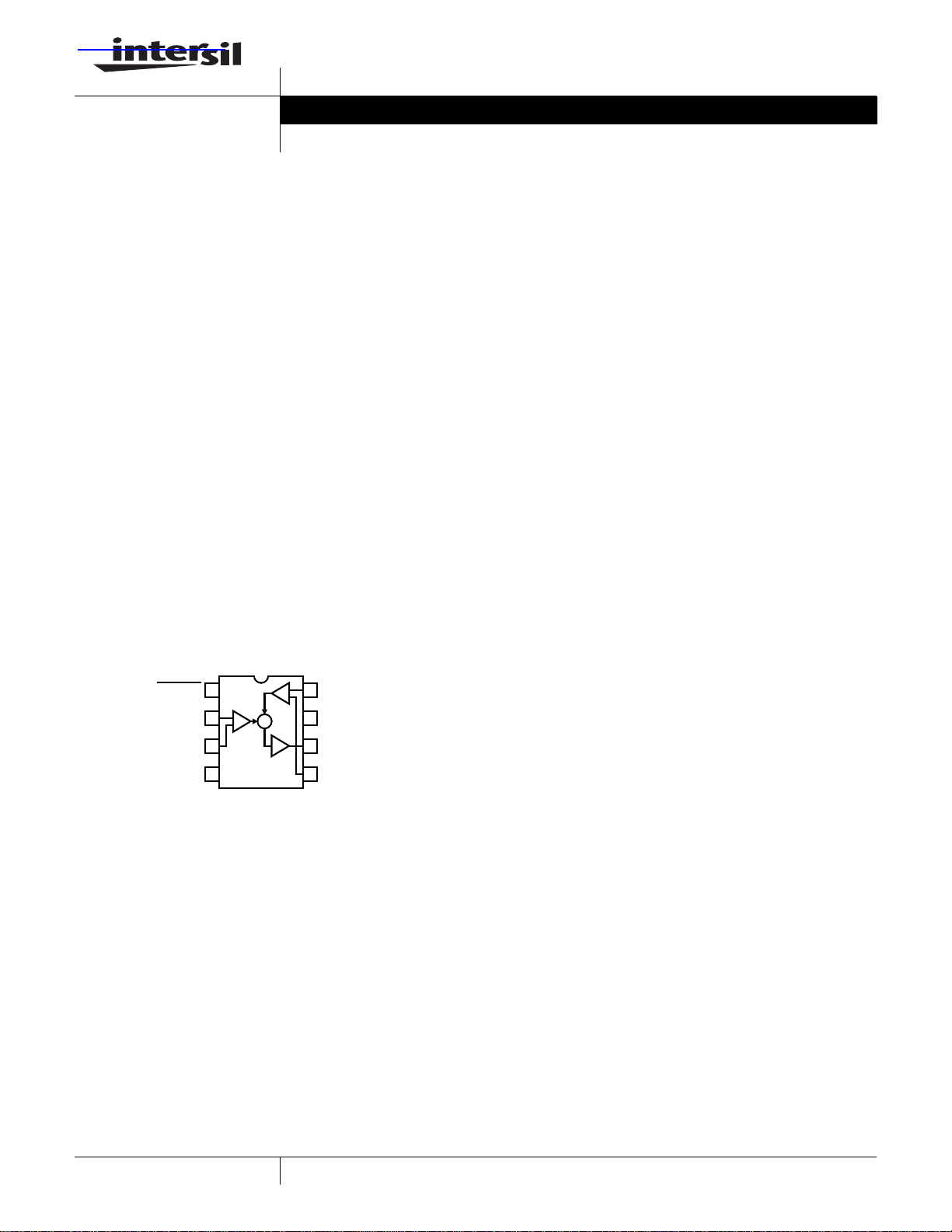
Pinout
EL8171, EL8172
(8 LD SO)
TOP VIEW
ENABLE
IN-
IN+
1
2
+
3
+
8
FB+
-
-
7
Σ
VS+
OUT
6
FN6293.0
Features
• 78µA maximum supply current
• Maximum input offset voltage
- 300µV (EL8172)
- 1000µV (EL8171)
• 200pA maximum input bias current
• 3µV/°C offset voltage drift
• 450kHz -3dB bandwidth (G = 10)
• 170kHz -3dB bandwidth (G = 100)
• 0.5V/µs slew rate
• Single supply operation
- Input voltage range is rail-to-rail
- Output swings rail-to-rail
• Output sources and sinks ±29mA load current
• 0.2% gain accuracy
• Pb-free plus anneal available (RoHS compliant)
Applications
• Battery- or solar-powered systems
• Strain gauges
• Current monitors
• Thermocouple amplifiers
VS-
4
1
5
FB-
CAUTION: These devices are sensitive to electrostatic discharge; follow proper IC Handling Procedures.
1-888-INTERSIL or 1-888-468-3774
| Intersil (and design) is a registered trademark of Intersil Americas Inc.
All other trademarks mentioned are the property of their respective owners.
Copyright © Intersil Americas Inc. 2005. All Rights Reserved.
Ordering Information
EL8171, EL8172
PAR T
PART NUMBER
EL8171IS 8171IS - 8 Ld SO MDP0027 EL8172IS 8172IS - 8 Ld SO MDP0027
EL8171IS-T7 8171IS 7” 8 Ld SO MDP0027 EL8172IS-T7 8172IS 7” 8 Ld SO MDP0027
EL8171IS-T13 8171IS 13” 8 Ld SO MDP0027 EL8172IS-T13 8172IS 13” 8 Ld SO MDP0027
EL8171ISZ
(See Note)
EL8171ISZ-T7
(See Note)
EL8171ISZ-T13
(See Note)
NOTE: Intersil Pb-free plus anneal products employ special Pb-free material sets; molding compounds/die attach materials and 100% matte tin plate
termination finish, which are RoHS compliant and compatible with both SnPb and Pb-free soldering operations. Intersil Pb-free products are MSL
classified at Pb-free peak reflow temperatures that meet or exceed the Pb-free requirements of IPC/JEDEC J STD-020.
MARKING
8171ISZ - 8 Ld SO
8171ISZ 7” 8 Ld SO
8171ISZ 13” 8 Ld SO
TAPE &
REEL PACKAGE
(Pb-free)
(Pb-free)
(Pb-free)
PKG.
DWG. # PART NUMBER
MDP0027 EL8172ISZ
(See Note)
MDP0027 EL8172ISZ-T7
(See Note)
MDP0027 EL8172ISZ-T13
(See Note)
PAR T
MARKING
8172ISZ - 8 Ld SO
8172ISZ 7” 8 Ld SO
8172ISZ 13” 8 Ld SO
TAPE &
REEL PACKAGE
(Pb-free)
(Pb-free)
(Pb-free)
PKG.
DWG. #
MDP0027
MDP0027
MDP0027
Pin Description
EL8171/EL8172 PIN NAME PIN FUNCTION
1 ENABLE
2 IN- Inverting (IN-) and non-inverting (IN+) high impedance input terminals. The input terminals are equivalent to
3IN+
5 FB- High impedance feedback terminals. The feedback terminals have a very similar equivalent circuit as the
8FB+
7 VS+ Positive supply terminal.
4 VS- Negative supply terminal.
6 VOUT Output Voltage.
Active Low. When pulled up above 2V, the in-amp conserves 3µA disabled supply current and the output is
in a high impedance state. An internal pull down defines the ENABLE
the gate of PMOS transistor.
input terminals. The negative feedback (FB-) pin connects to an external resistive network to set the gain of
the in-amp. The positive feedback (FB+) pin can be used to shift the DC level of the output or as an output
offset.
low when left floating.
2
FN6293.0
October 26, 2005
EL8171, EL8172
Absolute Maximum Ratings (T
Supply Voltage, V
Differential Input Current . . . . . . . . . . . . . . . . . . . . . . . . . . . . . . 5mA
Differential Input Voltage . . . . . . . . . . . . . . . . . . . . . . . . . . . . . . . . 5V
V
. . . . . . . . . . . . . . . . . . . . . . . . . . . . . . . . . . .0.5V to VS+ + 0.5V
EN
ESD . . . . . . . . . . . . . . . . . . . . . . . . . . . . . . . . . . . . . . . . . . . . . . . 3kV
CAUTION: Stresses above those listed in “Absolute Maximum Ratings” may cause permanent damage to the device. This is a stress only rating and operation of the
device at these or any other conditions above those indicated in the operational sections of this specification is not implied.
IMPORTANT NOTE: All parameters having Min/Max specifications are guaranteed. Typical values are for information purposes only. Unless otherwise noted, all tests
are at the specified temperature and are pulsed tests, therefore: TJ = TC = T
. . . . . . . . . . . . . . . . . . . . . . . . . . . . . . . . . . 5.5V
S
Electrical Specifications V
= 25°C)
A
Output Short-Circuit Duration . . . . . . . . . . . . . . . . . . . . . . .Indefinite
Ambient Operating Temperature . . . . . . . . . . . . . . . . -40°C to +85°C
Storage Temperature . . . . . . . . . . . . . . . . . . . . . . . .-65°C to +150°C
A
+ = +5V, VS- = GND, VCM = 1/2VS+ TA = 25°C, unless otherwise specified.
S
PARAMETER DESCRIPTION CONDITIONS MIN TYP MAX UNIT
V
OS
Input Offset Voltage EL8171 400 1000 µV
EL8172 150 300 µV
TCV
OS
Input Offset Voltage Temperature
Temperature = -40°C to 85°C 3 µV/°C
Coefficient
I
OS
I
B
e
N
Input Offset Current 10 200 pA
Input Bias Current 10 200 pA
Input Noise Voltage EL8171 f = 0.1Hz to 10Hz 10 µV
EL8172 4 µV
P-P
P-P
Input Noise Voltage Density fo = 1kHz 50 nV/√Hz
R
IN
V
IN
CMRR Common Mode Rejection Ratio EL8172, V
Input Resistance 25 GΩ
Input Voltage Range Guaranteed by CMRR test 0 5 V
= 0V to +5V 80 108 dB
CM
EL8171, V
= 0V to +5V 80 104 dB
CM
PSRR Power Supply Rejection Ratio EL8172, VS = 2.4V to 5V 80 104 dB
E
V
G
OUT
EL8171, V
Gain Error EL8172, RL = 100kΩ to 2.5V -1.5 +0.3 +1.5 %
EL8171, R
Maximum Voltage Swing Output low, 100kΩ to 2.5V 0 4 10 mV
= 2.4V to 5V 70 90 dB
S
= 100kΩ to 2.5V -0.8 +0.2 +0.8 %
L
Output low, 1kΩ to 2.5V 0.13 0.25 V
Output high, 100kΩ to 2.5V 4.990 4.996 V
Output high, 1kΩ to GND 4.75 4.88 V
SR Slew Rate R
= 1kΩ to GND 0.3 0.5 0.7 V/µs
L
-3dB BW -3dB Bandwidth EL8171 Gain = 10V/V 450 kHz
Gain = 20 210 kHz
Gain = 50 66 kHz
Gain = 100 33 kHz
EL8172 Gain = 100 172 kHz
Gain = 200 70 kHz
Gain = 500 25 kHz
Gain = 1000 12 kHz
I
S,EN
Supply Current, Enabled 40 60 78 µA
3
FN6293.0
October 26, 2005
EL8171, EL8172
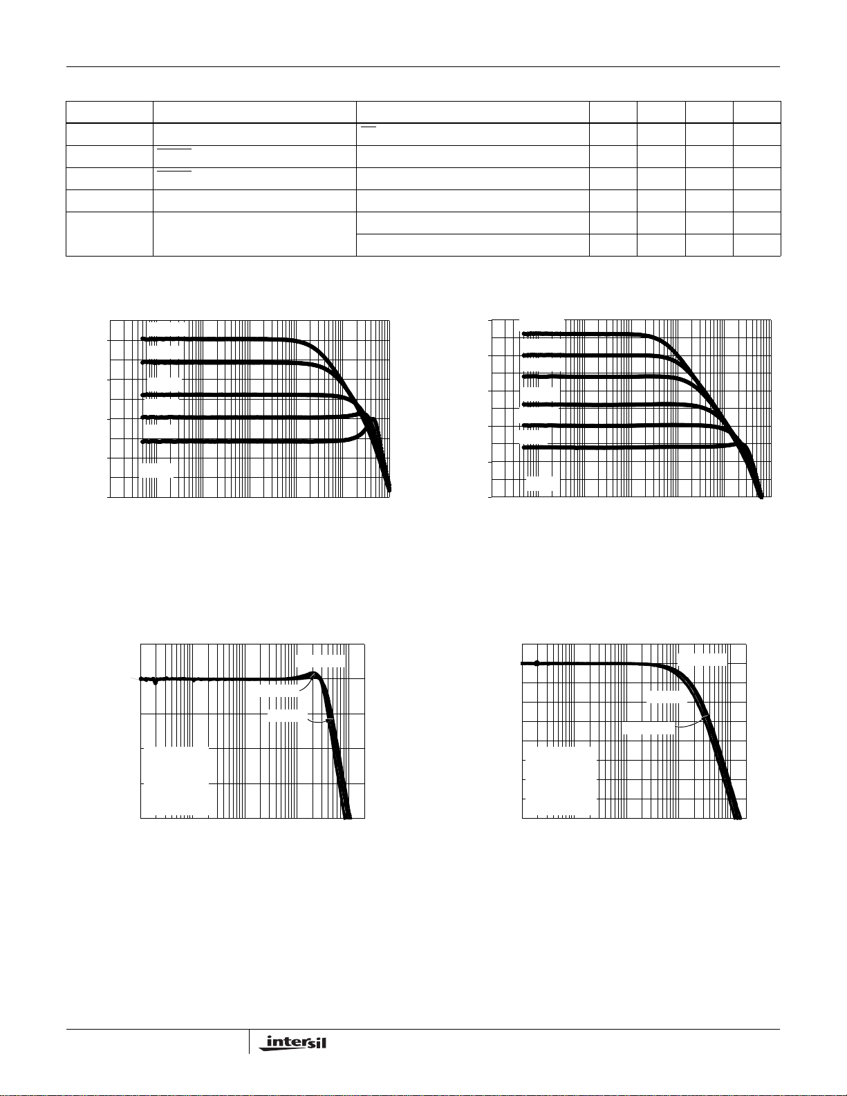
Electrical Specifications V
+ = +5V, VS- = GND, VCM = 1/2VS+ TA = 25°C, unless otherwise specified. (Continued)
S
PARAMETER DESCRIPTION CONDITIONS MIN TYP MAX UNIT
I
S,DIS
V
ENH
V
ENL
V
S
I
O
Supply Current, Disabled EN = VS+1.52.95µA
Enable Pin for Shut-down 2 V
Enable Pin for Power-on 0.8 V
Minimum Supply Voltage 2.2 2.4 V
Output Current into 10Ω to VS/2 VS = 5V ±18 ±29 mA
V
= 2.9V ±4 ±7.5 mA
S
Typical Performance Curves
40
30
20
GAIN (dB)
10
0
1 10 100 1K 10K 100K 1M
G=100
G=50
G=20
G=10
G=5
Vs=5V
FREQUENCY (Hz)
FIGURE 1. EL8171 FREQUENCY RESPONSE vs CLOSED
LOOP GAIN
70
60
50
GAIN (dB)
40
30
20
FIGURE 2. EL8172 FREQUENCY RESPONSE vs CLOSED
G=2000
G=1000
G=500
G=200
G=100
G=50
Vs=5V
1 10 100 1K 10K 100K 1M
FREQUENCY (Hz)
LOOP GAIN
25
VS=±2.5V
20
15
10
GAIN (dB)
AV=10
=10kΩ
R
L
CL=10pF
5
0
100 10k1k 100k
=9.08Ω
R
F/RG
RF=178kΩ
RG=19.6kΩ
VS=±1.25V
VS=±1V
1M
FREQUENCY (Hz)
FIGURE 3. EL8171 FREQUENCY RESPONSE vs SUPPLY
VO LTAGE
4
45
40
35
30
25
20
AV=100
15
=10kΩ
R
MAGNITUDE (dB)
L
CL=10pF
10
5
0
100 10k1k 100k
=99.02Ω
R
F/RG
RF=221kΩ
RG=2.23kΩ
FREQUENCY (Hz)
VS=±1.25V
VS=±2.5V
VS=±1V
1M
FIGURE 4. EL8172 FREQUENCY RESPONSE vs SUPPLY
VOLTAGE
FN6293.0
October 26, 2005

Typical Performance Curves (Continued)
EL8171, EL8172
30
25
20
15
AV=10
10
=5V
V
MAGNITUDE (dB)
S
=10kΩ
R
L
RF/RG=9.08Ω
5
RF=178kΩ
RG=19.6kΩ
0
100 10k1k 100k
CL=47pF
FREQUENCY (Hz)
FIGURE 5. EL8171 FREQUENCY RESPONSE vs C
4
25C
25°C
2
0
(pA)
-2
AVERAGE INPUT BIAS CURRENT
-4
-0.5 0 0.5 1 1.5 2 2.5 3 3.5 4 4.5 5 5.5
Vs=2.9V
Vs=3.3V
COMMON-MODE INPUT VOLTAGE (V)
CL=100pF
CL=27pF
1M
LOAD
Vs=5V
FIGURE 7. EL8171 AND EL8172 AVERAGE INPUT BIAS
CURRENT vs COMMON-MODE INPUT VOLTAGE
@ 25°C
50
45
CL=1000pF
40
CL=820pF
35
AV=100
=5V
V
MAGNITUDE (dB)
S
=10kΩ
R
L
30
RF/RG=99.02Ω
RF=221kΩ
RG=2.23kΩ
25
100 10k1k 100k
FREQUENCY (Hz)
FIGURE 6. EL8172 FREQUENCY RESPONSE vs C
4
-45°C
-45C
2
0
(pA)
-2
Vs=2.9V
CL=2200pF
CL=390pF
1M
LOAD
Vs=3.3V
Vs=5V
AVERAGE INPUT BIAS CURRENT
-4
-0.500.511.522.533.544.555.5
COMMON-MODE INPUT VOLTAGE (V)
FIGURE 8. EL8171 AND EL8172 AVERAGE INPUT BIAS
CURRENT vs COMMON-MODE INPUT VOLTAGE
@ -45°C
100
85°C
85C
50
Vs=5V
0
(pA)
-50
AVERAGE INPUT BIAS CURRENT
-100
-0.5 0 0.5 1 1.5 2 2.5 3 3.5 4 4.5 5 5.5
COMMON-MODE INPUT VOLTAGE (V)
Vs=2.9V
Vs=3.3V
FIGURE 9. EL8171 AND EL8172 AVERAGE INPUT BIAS
CURRENT vs COMMON-MODE INPUT VOLTAGE
@ 85°C
5
10
Vs=5V
5
0
-5
INPUT OFFSET CURRENT (pA)
-10
-0.500.511.522.533.544.555.5
COMMON-MODE INPUT VOLTAGE (V)
FIGURE 10. EL8171 AND EL8172 INPUT OFFSET CURRENT
vs COMMON-MODE INPUT VOLTAGE
FN6293.0
October 26, 2005

Typical Performance Curves (Continued)
EL8171, EL8172
600
500
400
300
200
100
INPUT OFFSET VOLTAGE (uV)
0
-0.500.511.522.533.544.555.5
25°C
25C
Vs=2.9V
COMMON-MODE INPUT VOLTAGE (V)
Vs=3.3V
Vs=5.0V
FIGURE 11. EL8171 INPUT OFFSET VOLTAGE vs COMMON-
MODE INPUT VOLTAGE @ 25°C
600
-45°C
500
400
300
-45C
Vs=5.0V
200
100
0
-100
INPUT OFFSET VOLTAGE (uV)
-200
-0.5 0 0.5 1 1.5 2 2.5 3 3.5 4 4.5 5 5.5
25°C
25C
Vs=5V
Vs=2.9V
Vs=3.3V
COMMON-MODE INPUT VOLTAGE (V)
FIGURE 12. EL8172 INPUT OFFSET VOLTAGE vs COMMON-
MODE INPUT VOLTAGE @ 25°C
100
-45°C
-45C
0
Vs=5V
-100
200
100
INPUT OFFSET VOLTAGE (uV)
0
-0.500.511.522.533.544.555.5
COMMON-MODE INPUT VOLTAGE (V)
Vs=2.9V
Vs=3.3V
FIGURE 13. EL8171 INPUT OFFSET VOLTAGE vs COMMON-
MODE INPUT VOLTAGE @ -45°C
800
700
600
500
400
300
INPUT OFFSET VOLTAGE (uV)
200
85°C
85C
Vs=2.9V
Vs=3.3V
-0.500.511.522.533.544.555.5
COMMON-MODE INPUT VOLTAGE (V)
Vs=5.0V
FIGURE 15. EL8171 INPUT OFFSET VOLTAGE vs COMMON-
MODE INPUT VOLTAGE @ 85°C
-200
INPUT OFFSET VOLTAGE (uV)
-300
-0.5 0.0 0.5 1.0 1.5 2.0 2.5 3.0 3.5 4.0 4.5 5.0 5.5
COMMON-MODE INPUT VOLTAGE (V)
Vs=2.9V
Vs=3.3V
FIGURE 14. EL8172 INPUT OFFSET VOLTAGE vs COMMON-
MODE INPUT VOLTAGE @ -45°C
500
85°C
85C
400
300
200
INPUT OFFSET VOLTAGE (uV)
100
-0.5 0.0 0.5 1.0 1.5 2.0 2.5 3.0 3.5 4.0 4.5 5.0 5.5
COMMON-MODE INPUT VOLTAGE (V)
Vs=5V
Vs=3.3VVs=2.9V
FIGURE 16. EL8172 INPUT OFFSET VOLTAGE vs COMMON-
MODE INPUT VOLTAGE @ 85°C
6
FN6293.0
October 26, 2005

Typical Performance Curves (Continued)
EL8171, EL8172
120
110
100
90
80
70
CMRR (dB)
60
50
40
1 10 100 1K 100K 1M10K
FREQUENCY (Hz)
GAIN=100
GAIN=10
120
110
100
90
80
70
CMRR (dB)
60
50
40
1 10 100 1K 100K 1M10K
GAIN=1000
GAIN=100
FREQUENCY (Hz)
FIGURE 17. EL8171 CMRR vs FREQUENCY FIGURE 18. EL8172 CMRR vs FREQUENCY
PSRR (dB)
100
PSRR+
80
PSRR-
60
PSRR (dB)
120
100
80
60
PSRR-
PSRR+
40
1 10 100 1K 10K 100K 1M
FREQUENCY (Hz)
FIGURE 19. EL8171 PSRR vs FREQUENCY FIGURE 20. EL8172 PSRR vs FREQUENCY
5uV/DIV
1s/DIV
FIGURE 21. EL8171 0.1Hz to 10Hz INPUT VOLTAGE NOISE
(GAIN = 10)
40
1 10 100 1K 10K 100K 1M
FREQUENCY (Hz)
1uV/DIV
1s/DIV
FIGURE 22. EL8172 0.1Hz to 10Hz INPUT VOLTAGE NOISE
(GAIN = 100)
7
FN6293.0
October 26, 2005

Typical Performance Curves (Continued)
70
60
50
40
30
20
SUPPLY CURRENT (µA)
10
0
23.52.5 4.5
FIGURE 23. EL8171 AND EL8172 SUPPLY CURRENT vs SUPPLY VOLTAGE
EL8171, EL8172
435
SUPPLY VOLTAGE (V)
5.5
JEDEC JESD51-7 HIGH EFFECTIVE THERMAL
CONDUCTIVITY TEST BOARD
1.4
1.2
1
909mW
0.8
0.6
0.4
POWER DISSIPATION (W)
0.2
0
0 25 50 75 100 150
θ
S
O
J
A
8
=
1
1
0
°
C
/
W
AMBIENT TEMPERATURE (°C)
12585
FIGURE 24. PACKAGE POWER DISSIPATION vs AMBIENT
TEMPERATURE
JEDEC JESD51-3 LOW EFFECTIVE THERMAL
CONDUCTIVITY TEST BOARD
1
0.9
0.8
0.7
625mW
0.6
0.5
0.4
0.3
0.2
POWER DISSIPATION (W)
0.1
0
0 25 50 75 100 150
S
θ
O
J
A
8
=
1
6
0
°
C
/
W
AMBIENT TEMPERATURE (°C)
12585
FIGURE 25. PACKAGE POWER DISSIPATION vs AMBIENT
TEMPERATURE
8
FN6293.0
October 26, 2005

EL8171, EL8172
Description of Operation and Application
Information
Product Description
The EL8171 and EL8172 are micropower instrumentation
amplifiers (in-amps) which deliver rail-to-rail input
amplification and rail-to-rail output swing on a single 2.4V to
5V supply. The EL8171 and EL8172 also deliver excellent
DC and AC specifications while consuming only 60µA typical
supply current. Because EL8171 and EL8172 provide an
independent pair of feedback terminals to set the gain and to
adjust the output level, these in-amps achieve high commonmode rejection ratio regardless of the tolerance of the gain
setting resistors. The EL8171 is internally compensated for a
minimum closed loop gain of 10 or greater, well suited for
moderate to high gains. For higher gains, the EL8172 is
internally compensated for a minimum gain of 100. An
ENABLE
2.9µA, while the instrumentation amplifier is disabled.
Input Protection
All input and feedback terminals of the EL8171 and EL8172
have internal ESD protection diodes to both positive and
negative supply rails, limiting the input voltage to within one
diode drop beyond the supply rails. If overdriving the inputs
is necessary, the external input current must never exceed
5mA. External series resistor may be used as a protection to
limit excessive external voltage and current from damaging
the inputs.
Input Stage and Input Voltage Range
The input terminals (IN+ and IN-) of the EL8171 and EL8172
are single differential pair P-MOSFET devices aided by an
Input Range Enhancement Circuit to increase the headroom
of operation of the common-mode input voltage. The
feedback terminals (FB+ and FB-) also have a similar
topology. As a result, the input common-mode voltage range
of both the EL8171 and EL8172 is rail-to-rail. These in-amps
are able to handle input voltages that are at or slightly
beyond the supply and ground making these in-amps well
suited for single 5V or 3.3V low voltage supply systems.
There is no need then to move the common-mode input of
the in-amps to achieve symmetrical input voltage.
Output Stage and Output Voltage Range
A pair of complementary MOSFET devices drives the output
VOUT to within a few mV of the supply rails. At a 100kΩ
load, the PMOS sources current and pulls the output up to
4mV below the positive supply, while the NMOS sinks
current and pulls the output down to 4mV above the negative
supply, or ground in the case of a single supply operation.
The current sinking and sourcing capability of the EL8171
and EL8172 are internally limited to 29mA.
Gain Setting
VIN, the potential difference across IN+ and IN-, is replicated
(less the input offset voltage) across FB+ and FB-. The
pin is used to reduce power consumption, typically
obsession of the EL8171 and EL8172 in-amp is to maintain
the differential voltage across FB+ and FB- equal to IN+ and
IN-; (FB+ - FB-) = (IN+ - IN-). Consequently, the transfer
function can be derived. The gain of the EL8171 and EL8172
is set by two external resistors, the feedback resistor RF, and
the gain resistor RG.
2.9V to 5V
1
VIN/2
VIN/2
VCM
RG
FIGURE 26. CIRCUIT 1 - GAIN IS BY EXTERNAL RESISTORS
R
AND R
VOUT 1
F
R
F
--------+
R
G
G
VIN=
7
VS+
IN+
2
+
IN-
3
-
FB+
8
+
FB-
5
-
EN
EL8171/2
VS-
4
RF
EN_BAR
6
VOUT
In Figure 26, the FB+ pin and one end of resistor RG are
connected to GND. With this configuration, the above gain
equation is only true for a positive swing in VIN; negative
input swings will be ignored and the output will be at ground.
Reference Connection
Unlike a three-opamp instrumentation amplifier, a finite
series resistance seen at the REF terminal does not degrade
the EL8171 and EL8172's high CMRR performance
eliminating the need for an additional external buffer
amplifier. Circuit 2 (Figure 27) uses the FB+ pin to provide a
high impedance REF terminal.
2.9V to 5V
1
VIN/2
VIN/2
VCM
2.9V to 5V
R1
REF
R2
FIGURE 27. CIRCUIT 2 - GAIN SETTING AND REFERENCE
VOUT 1
RG
CONNECTION
R
F
--------+
R
G
VIN()1
7
VS+
IN+
2
+
IN-
3
-
FB+
8
+
FB-
5
-
R
F
--------+
R
G
EN
EL8171/2
VS-
4
RF
VREF()+=
EN_BAR
6
VOUT
9
FN6293.0
October 26, 2005

EL8171, EL8172
The FB+ pin is used as a REF terminal to center or to adjust
the output. Because the FB+ pin is a high impedance input,
an economical resistor divider can be used to set the voltage
at the REF terminal without degrading or affecting the CMRR
performance. Any voltage applied to the REF terminal will
shift VOUT by VREF times the closed loop gain, which is set
by resistors RF and RG. See Circuit 2 (Figure 27).
The FB+ pin can also be connected to the other end of
resistor, RG. See Circuit 3 (Figure 28). Keeping the basic
concept that the EL8171 and EL8172 in-amps maintain
constant differential voltage across the input terminals and
feedback terminals (IN+ - IN- = FB+ - FB-), the transfer
function of Circuit 3 can be derived.
2.9V to 5V
1
VIN/2
VIN/2
VCM
VREF
FIGURE 28. CIRCUIT 3 - REFERENCE CONNECTION WITH AN
AVAILABLE VREF
R
VOUT 1
F
--------+
R
G
2
3
8
5
RG
VIN()VREF()+=
IN+
IN-
FB+
FB-
7
VS+
+
EL8171/2
+
-
VS-
4
RF
EN
EN_BAR
6
VOUT
error due to the tolerance of the resistors used. The resulting
non-ideal transfer function effectively becomes:
R
VOUT 1
F
--------+
1E
R
G
++()–[]VIN××=
RGERFEG
Where:
ERG = Tolerance of RG
ERF = Tolerance of RF
EG = Gain Error of the EL8171 or EL8172
The term [1-(ERG +ERF +EG)] is the deviation from the
theoretical gain. Thus, (ERG +ERF +EG) is the total gain
error. For example, if 1% resistors are used for the EL8171,
the total gain error would be:
E
RGERFEG
0.01 0.01 0.003++()±=
2.3%±=
typical()++()±=
Disable/Power-Down
The EL8171 and EL8172 can be powered down reducing
the supply current to typically 2.9µA. When disabled, the
output is in a high impedance state. The active low ENABLE
bar pin has an internal pull down and hence can be left
floating and the in-amp enabled by default. When the
ENABLE
will power down when ENABLE
will power on when ENABLE
bar is connected to an external logic, the in-amp
bar is pulled above 2V, and
bar is pulled below 0.8V.
A finite resistance Rs in series with the VREF source, adds
an output offset of VIN*(RS/RG). As the series resistance Rs
approaches zero, the gain equation is simplified to the above
equation for Circuit 3. VOUT is simply shifted by an amount
VREF.
External Resistor Mismatches
Because of the independent pair of feedback terminals
provided by the EL8171 and EL8172, the CMRR is not
degraded by any resistor mismatches. Hence, unlike a three
opamp and especially a two opamp in-amp, the EL8171 and
EL8172 reduce the cost of external components by allowing
the use of 1% or more tolerance resistors without sacrificing
CMRR performance. The EL8171 and EL8172 CMRR will be
108dB regardless of the tolerance of the resistors used.
Gain Error and Accuracy
The EL8172 has a Gain Error, EG, of 0.2% typical. The
EL8171 has an EG of 0.3% typical. The gain error indicated
in the electrical specifications table is the inherent gain error
of the EL8171 and EL8172 and does not include the gain
error contributed by the resistors. There is an additional gain
10
FN6293.0
October 26, 2005

Package Outline Drawing
EL8171, EL8172
NOTE: The package drawing shown here may not be the latest version. To check the latest revision, please refer to the Intersil website at
http://www.intersil.com/design/packages/index.asp
All Intersil U.S. products are manufactured, assembled and tested utilizing ISO9000 quality systems.
Intersil Corporation’s quality certifications can be viewed at www.intersil.com/design/quality
Intersil products are sold by description only. Intersil Corporation reserves the right to make changes in circuit design, software and/or specifications at any time without
notice. Accordingly, the reader is cautioned to verify that data sheets are current before placing orders. Information furnished by Intersil is believed to be accurate and
reliable. However, no responsibility is assumed by Intersil or its subsidiaries for its use; nor for any infringements of patents or other rights of third parties which may result
from its use. No license is granted by implication or otherwise under any patent or patent rights of Intersil or its subsidiaries.
For information regarding Intersil Corporation and its products, see www.intersil.com
11
FN6293.0
October 26, 2005
 Loading...