

®
EL8171, EL8172
Data Sheet July 27, 2009
Micropower, Single Supply, Rail-to-Rail
Input-Output Instrumentation Amplifiers
The EL8171 and EL8172 are micropower instrumentation
amplifiers optimized for single supply operation over the
+2.4V to +5.5V range. Inputs and outputs can operate
rail-to-rail. As with all instrumentation amplifiers, a pair of
inputs provide very high common-mode rejection and are
completely independent from a pair of feedback terminals.
The feedback terminals allow zero input to be translated to
any output offset, including ground. A feedback divider
controls the overall gain of the amplifier.
The EL8172 is compensated for a gain of 100 or more, and
the EL8171 is compensated for a gain of 10 or more. The
EL8171 and EL8172 have PMOS input devices that provide
sub-nA input bias currents.
The amplifiers can be operated from one lithium cell or two
Ni-Cd batteries. The EL8171 and EL8172 input range goes
from below ground to slightly above positive rail. The output
stage swings completely to ground (ground sensing) or
positive supply - no pull-up or pull-down resistors are
needed.
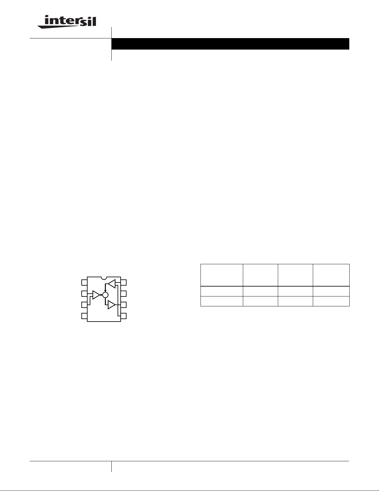
Pinout
EL8171, EL8172
(8 LD SOIC)
TOP VIEW
DNC
IN-
IN+
1
2
+
3
V-
4
+
8
FB+
-
-
Σ
7
6
5
V+
VOUT
FB-
FN6293.5
Features
• 95µA maximum supply current
• Maximum input offset voltage
- 300µV (EL8172)
- 1500µV (EL8171)
• 50pA maximum input bias current
• 450kHz -3dB bandwidth (G = 10)
• 170kHz -3dB bandwidth (G = 100)
• Single supply operation
- Input voltage range is rail-to-rail
- Output swings rail-to-rail
- Ground sensing
• Pb-free (RoHS compliant)
Applications
• Battery- or solar-powered systems
• Strain gauges
• Current monitors
• Thermocouple amplifiers
Ordering Information
PART
NUMBER
(Note)
EL8171FSZ* 8171FSZ 8 Ld SOIC MDP0027
EL8172FSZ* 8172FSZ 8 Ld SOIC MDP0027
*Add “-T7” suffix for tape and reel. Please refer to TB347 for details
on reel specifications.
NOTE: These Intersil Pb-free plastic packaged products employ
special Pb-free material sets, molding compounds/die attach
materials, and 100% matte tin plate plus anneal (e3 termination
finish, which is RoHS compliant and compatible with both SnPb and
Pb-free soldering operations). Intersil Pb-free products are MSL
classified at Pb-free peak reflow temperatures that meet or exceed
the Pb-free requirements of IPC/JEDEC J STD-020.
PART
MARKING
PACKAGE
(Pb-free)
PKG.
DWG. #
1
CAUTION: These devices are sensitive to electrostatic discharge; follow proper IC Handling Procedures.
1-888-INTERSIL or 1-888-468-3774
| Intersil (and design) is a registered trademark of Intersil Americas Inc.
Copyright © Intersil Americas Inc. 2005-2007, 2009. All Rights Reserved.
All other trademarks mentioned are the property of their respective owners.
EL8171, EL8172
Absolute Maximum Ratings (T
Supply Voltage, V+ . . . . . . . . . . . . . . . . . . . . . . . . . . . . . . . . . . 5.5V
Differential Input Current . . . . . . . . . . . . . . . . . . . . . . . . . . . . . . 5mA
Differential Input Voltage (EL8172) . . . . . . . . . . . . . . . . . . . . . . 0.5V
Differential Input Voltage (EL8171) . . . . . . . . . . . . . . . . . . . . . . 1.0V
ESD Rating
Human Body Model . . . . . . . . . . . . . . . . . . . . . . . . . . . . . . . . .3kV
= +25°C) Thermal Information
A
Thermal Resistance θ
8 Ld SOIC Package . . . . . . . . . . . . . . . . . . . . . . . . 122
Output Short-Circuit Duration . . . . . . . . . . . . . . . . . . . . . . .Indefinite
Ambient Operating Temperature . . . . . . . . . . . . . . .-40°C to +125°C
Storage Temperature. . . . . . . . . . . . . . . . . . . . . . . .-65°C to +150°C
Pb-Free Reflow Profile. . . . . . . . . . . . . . . . . . . . . . . . .see link below
(°C/W)
JA
http://www.intersil.com/pbfree/Pb-FreeReflow.asp
CAUTION: Do not operate at or near the maximum ratings listed for extended periods of time. Exposure to such conditions may adversely impact product reliability and
result in failures not covered by warranty.
IMPORTANT NOTE: All parameters having Min/Max specifications are guaranteed. Typical values are for information purposes only. Unless otherwise noted, all tests
are at the specified temperature and are pulsed tests, therefore: TJ = TC = T
Electrical Specifications V
= +5V , V- = GND, VCM = 1/2V+, RL = Open, TA = +25°C, unless otherwise specified. Boldface limits apply
+
over the operating temperature range, -40°C to +125°C.
PARAMETER DESCRIPTION CONDITIONS
A
MIN
(Note 1) TYP
MAX
(Note 1) UNIT
DC SPECIFICATIONS
V
OS
Input Offset Voltage EL8171 -1.5-2±0.47 1.5
mV
2
TCV
OS
Input Offset Voltage Temperature
Coefficient
I
I
V
OS
B
IN
Input Offset Current, ± IN, ± FB -25
Input Bias Current -50
Input Voltage Range Guaranteed by CMRR test 0 5 V
CMRR Common Mode Rejection Ratio V
EL8172 -0.3
-0.7
EL8171 1.5 µV/°C
EL8172 0.14 µV/°C
-500
= 0V to +5V 75 100 dB
CM
-4
±0.07 0.3
0.7
±4 25
500
±10 50
mV
pA
pA
pA
4
nA
PSRR Power Supply Rejection Ratio EL8171, V+ = 2.4V to 5V 75 90 dB
E
G
V
OUT
I
S
V
SUPPLY
I
O+
EL8172, V
Gain Error EL8171, RL = 100kΩ to 2.5V -0.7 ±0.15 0.7 %
EL8172, R
Maximum Voltage Swing Output low, 100kΩ to 2.5V 4 10
Output low, 1kΩ to 2.5V 0.13 0.2
Output high, 100kΩ to 2.5V 4.985
Output high, 1kΩ to GND 4.860
Supply Current 45
Supply Operating Range V+ to V- 2.4 5.5 V
Output Source Current into 10Ω to V+/2 V+ = 5V 23
= 2.4V to 5V 75 100 dB
+
= 100kΩ to 2.5V -1
L
-1.5
±0.2 +1
1.5
10
0.25
4.996 V
4.980
4.87 V
4.750
65 95
38
110
32 mA
%
%
mV
mV
V
V
V
V
µA
19
V
= 2.4V 6
+
4.5
8mA
2
FN6293.5
July 27, 2009
EL8171, EL8172
Electrical Specifications V
PARAMETER DESCRIPTION CONDITIONS
I
O-
Output Sink Current into 10Ω to V+/2 V+ = 5V 19
= +5V , V- = GND, VCM = 1/2V+, RL = Open, TA = +25°C, unless otherwise specified. Boldface limits apply
+
over the operating temperature range, -40°C to +125°C. (Continued)
MIN
(Note 1) TYP
MAX
(Note 1) UNIT
26 mA
15
= 2.4V 5
V
+
4
7mA
AC SPECIFICATIONS
-3dB BW -3dB Bandwidth EL8171 Gain = 10V/V 450 kHz
Gain = 20 210 kHz
Gain = 50 66 kHz
Gain = 100 33 kHz
EL8172 Gain = 100 170 kHz
Gain = 200 70 kHz
Gain = 500 25 kHz
Gain = 1000 12 kHz
e
N
Input Noise Voltage EL8171 f = 0.1Hz to 10Hz 14 µV
EL8172 10 µV
P-P
P-P
Input Noise Voltage Density EL8171 fo = 1kHz 220 nV/√Hz
EL8172 80 nV/√Hz
i
N
CMRR @ 60Hz Input Common Mode Rejection Ratio EL8171 V
PSRR+ @
120Hz
PSRR- @
120Hz
Input Noise Current Density EL8171, fo = 1kHz 0.9 pA/√Hz
Power Supply Rejection Ratio (V
Power Supply Rejection Ratio (V
EL8172, f
EL8172 100 dB
) EL8171 V+, V- = ±2.5V,
+
EL8172 92 dB
) EL8171 V+, V- = ±2.5V,
-
EL8172 92 dB
= 1kHz 0.2 pA/√Hz
o
= 1VPP,
CM
R
= 10kΩ to V
L
CM
85 dB
90 dB
V
SOURCE
R
L
= 1VPP,
= 10kΩ to V
CM
97 dB
V
SOURCE
R
L
= 1VPP,
= 10kΩ to V
CM
TRANSIENT RESPONSE
SR Slew Rate R
= 1kΩ to GND 0.4
L
0.35
0.55 0.7
0.7
V/µs
NOTES:
1. Parameters with MIN and/or MAX limits are 100% tested at +25°C, unless otherwise specified. Temperature limits established by characterization
and are not production tested.
3
FN6293.5
July 27, 2009
EL8171, EL8172
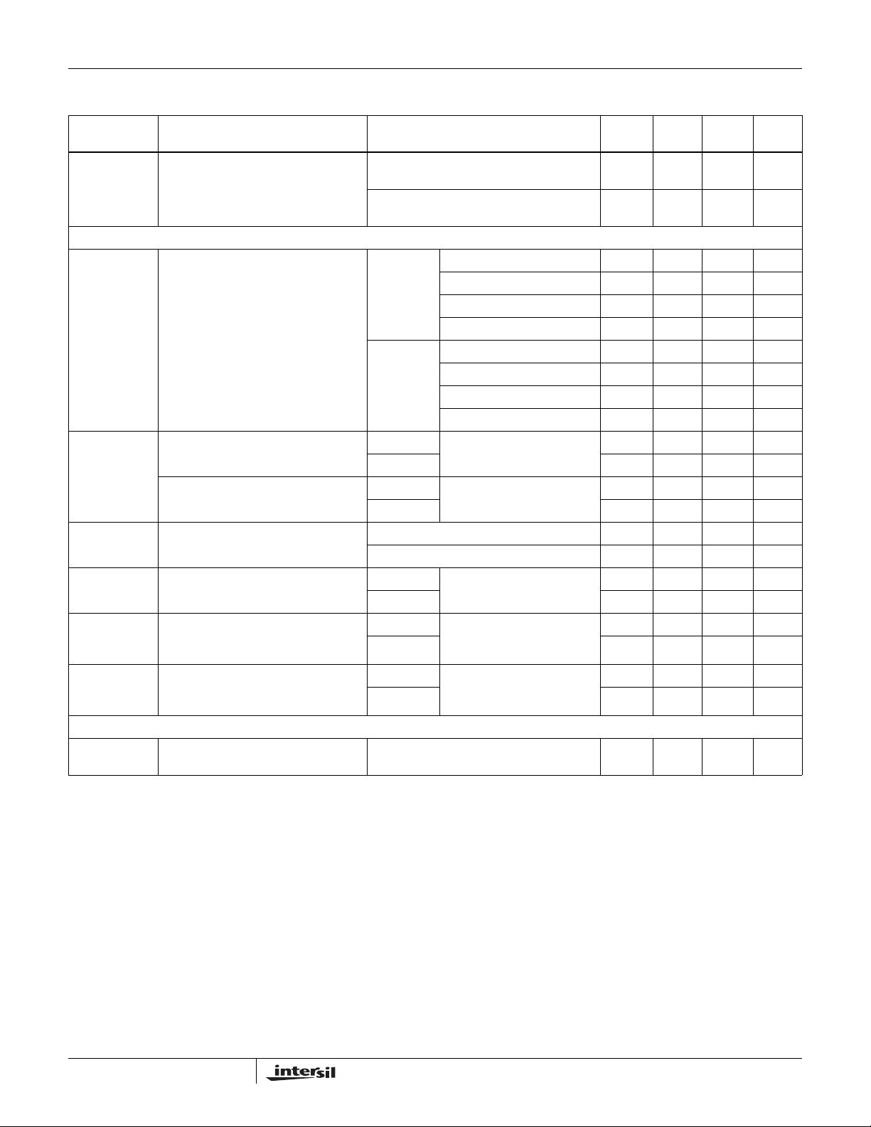
Typical Performance Curves V
70
60
50
40
GAIN (dB)
30
20
10
1 10 100 1k 10k 100k 1M
GAIN = 1000
GAIN = 500
GAIN = 200
GAIN = 100
GAIN = 50
GAIN = 20
GAIN = 10
COMMON-MODE INPUT = 1/2V+
FREQUENCY (Hz)
= 5V, V- = 0V,VCM = 2.5V, RL = Open, unless otherwise specified.
+
FIGURE 1. EL8171 FREQUENCY RESPONSE vs CLOSED
LOOP GAIN
25
20
15
10
GAIN (dB)
AV = 10
= 10kΩ
R
L
= 10pF
C
L
5
0
10
= 10
R
F/RG
= 1kΩ
R
F
= 100Ω
R
G
100 10k1k 100k 1M
FREQUENCY (Hz)
V
+
= 2.4V
V+ = 5V
FIGURE 3. EL8171 FREQUENCY RESPONSE vs SUPPLY
VOLTAGE
90
80
70
60
GAIN (dB)
50
40
30
GAIN = 10,000
GAIN = 5,000
GAIN = 2,000
GAIN = 1,000
GAIN = 500
GAIN = 200
GAIN = 100
1 10 100 1k 10k 100k 1M
COMMON-MODE INPUT = 1/2V+
FREQUENCY (Hz)
FIGURE 2. EL8172 FREQUENCY RESPONSE vs CLOSED
LOOP GAIN
45
40
35
30
25
20
GAIN (dB)
15
10
5
0
AV = 100
R
L
C
L
R
F/RG
R
F
R
G
10
= 10kΩ
= 10pF
= 100
= 10kΩ
= 100Ω
100 10k1k 100k 1M
FREQUENCY (Hz)
V
+
V+ = 5V
= 2.4V
FIGURE 4. EL8172 FREQUENCY RESPONSE vs SUPPLY
VOLTAGE
25
470pF
20
220pF
15
GAIN (dB)
AV = 10
= 10kΩ
R
10
= 10pF
C
L
= 10
R
F/RG
= 10kΩ
R
F
= 100Ω
R
G
5
10
100 10k1k 100k 1M
FREQUENCY (Hz)
FIGURE 5. EL8171 FREQUENCY RESPONSE vs C
4
820pF
100pF
LOAD
50
45
40
35
GAIN (dB)
AV = 10
= 10kΩ
R
= 10pF
C
L
30
25
10
= 10
R
F/RG
= 10kΩ
R
F
= 100Ω
R
G
100 10k1k 100k 1M
FREQUENCY (Hz)
820pF
FIGURE 6. EL8172 FREQUENCY RESPONSE vs C
2200pF
1200pF
56pF
LOAD
FN6293.5
July 27, 2009

EL8171, EL8172
Typical Performance Curves V
90
80
70
60
50
40
AV = 10
30
CMRR (dB)
20
10
0
-10
10 100 1k 10k 100k 1M
FREQUENCY (Hz)
FIGURE 7. EL8171 CMRR vs FREQUENCY
120
100
80
60
PSRR (dB)
40
20
AV = 10
PSRR-
= 5V, V- = 0V,VCM = 2.5V, RL = Open, unless otherwise specified. (Continued)
+
120
100
80
60
CMRR (dB)
40
20
AV = 100
0
10 100 1k 10k 100k 1M
FREQUENCY (Hz)
FIGURE 8. EL8172 CMRR vs FREQUENCY
120
100
PSRR+
80
60
PSRR (dB)
40
20
PSRR-
AV = 10
PSRR+
0
10 100 1k 10k 100k 1M
FREQUENCY (Hz)
FIGURE 9. EL8171 PSRR vs FREQUENCY
1400
1200
1000
800
600
400
200
INPUT VOLTAGE NOISE (nV/√Hz)
0
1 10 100 1k 10k 100k
AV = 10
FREQUENCY (Hz)
0
10 100 1k 10k 100k 1M
FREQUENCY (Hz)
FIGURE 10. EL8172 PSRR vs FREQUENCY
700
600
500
400
300
200
100
INPUT VOLTAGE NOISE (nV/√Hz)
0
1 10 100 1k 10k 100k
AV = 100
FREQUENCY (Hz)
FIGURE 11. EL8171 VOLTAGE NOISE SPECTRAL DENSITY FIGURE 12. EL8172 VOLTAGE NOISE SPECTRAL DENSITY
5
FN6293.5
July 27, 2009

EL8171, EL8172
Typical Performance Curves V
6
5
4
3
2
1
CURRENT NOISE (pA/√Hz)
0
1 10 100 1k 10k 100k
AV = 10
FREQUENCY (Hz)
= 5V, V- = 0V,VCM = 2.5V, RL = Open, unless otherwise specified. (Continued)
+
2.0
1.8
1.6
1.4
1.2
1.0
0.8
0.6
0.4
CURRENT NOISE (pA/√Hz)
0.2
0.0
1 10 100 1k
AV = 100
AV = 100
FREQUENCY (Hz)
10k
FIGURE 13. EL8171 CURRENT NOISE SPECTRAL DENSITY FIGURE 14. EL8172 CURRENT NOISE SPECTRAL DENSITY
100k
VOLTAGE NOISE (5µV/DIV)
TIME (1s/DIV)
FIGURE 15. EL8171 0.1Hz TO 10Hz INPUT VOLT AGE NOISE
(GAIN = 10)
80
N = 1000
75
70
65
60
55
50
SUPPLY CURRENT (μA)
45
40
-40 -20 0 20 40 60 80 100 120
TEMPERATURE (°C)
MAX
MEDIAN
MIN
FIGURE 17. EL8171 SUPPLY CURRENT vs TEMPERA TURE,
V
, V- = ±2.5V, VIN = 0V
+
VOLTAGE NOISE (2µV/DIV)
TIME (1s/DIV)
FIGURE 16. EL8172 0.1Hz TO 10Hz INPUT VOLTAGE NOISE
(GAIN = 100)
90
N = 1500
85
80
75
70
65
60
55
50
SUPPLY CURRENT (μA)
45
40
-40 -20 0 20 40 60 80 100 120
TEMPERATURE (°C)
MAX
MEDIAN
MIN
FIGURE 18. EL8172 SUPPLY CURRENT vs TEMPERA TURE,
V+, V- = ±2.5V, VIN = 0V
6
FN6293.5
July 27, 2009

EL8171, EL8172
Typical Performance Curves V
2.5
N = 1000
2.0
1.5
1.0
0.5
(µV)
OS
0
V
-0.5
-1.0
-1.5
-2.0
-40 -20 0 20 40 60 80 100 120
MAX
MEDIAN
TEMPERATURE (°C)
= 5V, V- = 0V,VCM = 2.5V, RL = Open, unless otherwise specified. (Continued)
+
MIN
FIGURE 19. EL8171 VOS vs TEMPERATURE, V+, V- = ±2.5V ,
V
= 0V
IN
2.5
N = 1000
2.0
1.5
1.0
0.5
(µV)
0
OS
V
-0.5
-1.0
-1.5
-2.0
-2.5
-40 -20 0 20 40 60 80 100 120
FIGURE 21. EL8171 V
V
= 0V
IN
MAX
MEDIAN
MIN
TEMPERATURE (°C)
vs TEMPERATURE, V+, V- = ±1.2V ,
OS
0.7
N = 1500
0.5
0.3
0.1
(µV)
OS
-0.1
V
-0.3
-0.5
-0.7
-40 -20 0 20 40 60 80 100 120
FIGURE 20. EL8172 V
V
= 0V
IN
0.9
N = 1500
0.7
0.5
0.3
(µV)
0.1
OS
V
-0.1
-0.3
-0.5
-0.7
-40 0 20 40 60 80 100 120-20
FIGURE 22. EL8172 V
V
= 0V
IN
MAX
MEDIAN
MIN
TEMPERATURE (°C)
vs TEMPERA TURE, V+, V- = ±2.5V ,
OS
MAX
MEDIAN
MIN
TEMPERATURE (°C)
vs TEMPERA TURE, V+, V- = ±1.2V ,
OS
140
N = 1000
130
120
110
CMRR (dB)
100
90
80
-40 -20 0 20 40 60 80 100 120
MAX
MEDIAN
MIN
TEMPERATURE (°C)
FIGURE 23. EL8171 CMRR vs TEMPERATURE,
V
= +2.5V TO -2.5V, V+, V- = ±2.5V
CM
7
140
N = 1500
130
120
110
CMRR (dB)
100
90
80
-40-200 20406080100120
MAX
MEDIAN
MIN
TEMPERATURE (°C)
FIGURE 24. EL8172 CMRR vs TEMPERATURE,
V
= +2.5V TO -2.5V, V+, V- = ±2.5V
CM
FN6293.5
July 27, 2009

EL8171, EL8172
Typical Performance Curves V
140
N = 1000
130
120
110
100
90
PSRR (dB)
80
70
60
-40-200 20406080100120
MAX
MEDIAN
MIN
TEMPERATURE (°C)
= 5V, V- = 0V,VCM = 2.5V, RL = Open, unless otherwise specified. (Continued)
+
FIGURE 25. EL8171 PSRR vs TEMPERATURE,
V
, V- = ±1.2V TO ±2.5V
+
0.7
N = 1000
0.6
0.5
0.4
0.3
0.2
GAIN ERROR (%)
0.1
0
-0.1
-40-200 20406080100120
TEMPERATURE (°C)
MAX
MEDIAN
MIN
FIGURE 27. EL8171% GAIN ERROR vs TEMPERATURE,
R
= 100k
L
140
N = 1500
130
120
110
100
90
PSRR (dB)
80
70
60
-40 -20 0 20 40 60 80 100 120
MAX
MEDIAN
MIN
TEMPERATURE (°C)
FIGURE 26. EL8172 PSRR vs TEMPERATURE,
V
, V- = ±1.2V TO ±2.5V
+
1.5
N = 1500
1.3
1.1
0.9
0.7
0.5
GAIN ERROR (%)
0.3
0.1
-0.1
-40-200 20406080100120
MAX
MEDIAN
MIN
TEMPERATURE (°C)
FIGURE 28. EL8172% GAIN ERROR vs TEMPERATURE,
RL = 100k
4.91
4.90
4.89
4.88
(V)
4.87
OUT
V
4.86
4.85
4.84
4.83
FIGURE 29. EL8171 V
N = 1000
MEDIAN
-40 -20 0 20 40 60 80 100 120
R
= 1k, V+, V- = ±2.5V
L
TEMPERATURE (°C)
HIGH vs TEMPERA TURE,
OUT
8
MIN
MAX
4.91
4.90
4.89
4.88
(V)
4.87
OUT
V
4.86
4.85
4.84
4.83
FIGURE 30. EL8172 V
N = 1500
MEDIAN
-40 -20 0 20 40 60 80 100 120
R
= 1k, V+, V- = ±2.5V
L
TEMPERATURE (°C)
HIGH vs TEMPERATURE,
OUT
MIN
MAX
FN6293.5
July 27, 2009

EL8171, EL8172
Typical Performance Curves V
200
N = 1000
180
160
(mV)
140
OUT
V
120
100
80
-40 -20 0 20 40 60 80 100 120
FIGURE 31. EL8171 V
0.65
0.60
0.55
0.50
0.45
0.40
+SLEW RATE (V/µs)
0.35
0.30
-40-200 20406080100120
MEDIAN
TEMPERATURE (°C)
R
N = 1000
OUT
= 1k, V+, V- = ±2.5V
L
TEMPERATURE (°C)
MAX
MIN
LOW vs TEMPERATURE,
MAX
MEDIAN
MIN
= 5V, V- = 0V,VCM = 2.5V, RL = Open, unless otherwise specified. (Continued)
+
FIGURE 33. EL8171 +SLEW RATE vs TEMPERATURE,
INPUT = ±0.015V @ GAIN + 100
180
N = 1000
170
160
150
140
(mV)
130
OUT
V
120
110
100
90
FIGURE 32. EL8172 V
0.60
0.58
0.56
0.54
0.52
0.50
0.48
0.46
+SLEW RATE (V/µs)
0.44
0.42
0.40
MEDIAN
-40 -20 0 20 40 60 80 100 120
R
N = 1500
-40 -20 0 20 40 60 80 100 120
OUT
= 1k, V+, V- = ±2.5V
L
MEDIAN
MAX
MIN
TEMPERATURE (°C)
LOW vs TEMPERA TURE,
MAX
MIN
TEMPERATURE (°C)
FIGURE 34. EL8172 +SLEW RATE vs TEMPERA TURE,
INPUT = ±0.015V @ GAIN + 100
0.70
N = 1000
0.65
0.60
0.55
0.50
0.45
0.40
- SLEW RATE (V/µS)
0.35
0.30
-40 -20 0 20 40 60 80 100 120
MAX
MEDIAN
MIN
TEMPERATURE (°C)
FIGURE 35. EL8171 -SLEW RATE vs TEMPERA TURE,
INPUT = ±0.015V @ GAIN + 100
9
0.65
N = 1500
0.60
0.55
0.50
-SLEW RATE (V/µS)
0.45
0.40
-40 -20 0 20 40
MAX
MEDIAN
MIN
60
TEMPERATURE (°C)
80 100 120
FIGURE 36. EL8172 -SLEW RATE vs TEMPERATURE,
INPUT = ±0.015V @ GAIN + 100
FN6293.5
July 27, 2009

EL8171, EL8172
Pin Descriptions
EL8171/EL8172 PIN NAME EQUIVALENT CIRCUIT PIN FUNCTION
1 DNC Do Not Connect; Internal connection - Must be left floating.
2 IN- Circuit 1A, Circuit 1B High impedance input terminals. EL8172 input circuit is shown in Circuit 1A, and
3 IN+ Circuit 1A, Circuit 1B
4 V- Circuit 3 Negative supply terminal.
5 FB- Circuit 1A, Circuit 1B High impedance feedback terminals. EL8172 input circuit is shown in Circuit 1A,
8 FB+ Circuit 1A, Circuit 1B
7 V+ Circuit 3 P ositive supply terminal.
6 VOUT Circuit 2 Output Voltage.
the EL8171 input circuit is shown in Circuit 1B. EL8171: to avoid offset drift, it is
recommended that the terminals are not overdriven beyond 1V and the input
current must never exceed 5mA.
and the EL8171 input circuit is shown in Circuit 1B. EL8171: to avoid offset drift, it
is recommended that the terminals are not overdriven beyond 1V and the input
current must never exceed 5mA.
V+
IN-
FB-
IN+
FB+
V-
CIRCUIT 1A
IN-
FB-
CIRCUIT 1B
Description of Operation and Application
Information
Product Description
The EL8171 and EL8172 are micropower instrumentation
amplifiers (in-amps) which deliver rail-to-rail input amplification
and rail-to-rail output swing on a single 2.4V to 5.5V supply. The
EL8171 and EL8172 also deliver excellent DC and AC
specifications while consuming only 65µA typical supply
current. Because EL8171 and EL8172 provide an independent
pair of feedback terminals to set the gain and to adjust the
output level, these in-amps achieve high common-mode
rejection ratio regardless of the tolerance of the gain setting
resistors. The EL8171 is internally compensated for a minimum
closed loop gain of 10 or greater, well suited for moderate to
high gains. For higher gains, the EL8172 is internally
compensated for a minimum gain of 100.
Input Protection
All input and feedback terminals of the EL8171 and EL8172
have internal ESD protection diodes to both positive and
negative supply rails, limiting the input voltage to within one
diode drop beyond the supply rails. The inverting inputs and
FB- inputs have ESD diodes to the V-rail, and the non-inverting
inputs and FB+ terminals have ESD diodes to the V+ rail. The
EL8172 has additional back-to-back diodes across the input
terminals and also across the feedback terminals. If overdriving
the inputs is necessary, the external input current must never
exceed 5mA. On the other hand, the EL8171 has no clamps to
limit the differential voltage on the input terminals allowing
V+
IN+
FB+
V-
V+
OUT
V-
CIRCUIT 2
V+
V-
CIRCUIT 3
CAPACITIVELY
COUPLED
ESD CLAMP
higher differential input voltages at lower gain applications. It is
recommended however, that the input terminals of the EL8171
are not overdriven beyond 1V to avoid offset drift. An external
series resistor may be used as an external protection to limit
excessive external voltage and current from damaging the
inputs.
Input Stage and Input Voltage Range
The input terminals (IN+ and IN-) of the EL8171 and EL8172
are single differential pair P-MOSFET devices aided by an
Input Range Enhancement Circuit (IREC) to increase the
headroom of operation of the common-mode input voltage.
The feedback terminals (FB+ and FB-) also have a similar
topology. As a result, the input common-mode voltage range
of both the EL8171 and EL8172 is rail-to-rail. These in-amps
are able to handle input voltages that are at or slightly
beyond the supply and ground making these in-amps well
suited for single 5V or 3.3V low voltage supply systems.
There is no need to move the common-mode input of the inamps to achieve symmetrical input voltage.
Output Stage and Output Voltage Range
A pair of complementary MOSFET devices drive the output
V
to within a few mV of the supply rails. At a 100kΩ load,
OUT
the PMOS sources current and pulls the output up to 4mV
below the positive supply, while the NMOS sinks current and
pulls the output down to 4mV above the negative supply, or
ground in the case of a single supply operation. The current
sinking and sourcing capability of the EL8171 and EL8172
are internally limited to less than 35mA.
10
FN6293.5
July 27, 2009

EL8171, EL8172
Gain Setting
VIN, the potential difference across IN+ and IN-, is replicated
(less the input offset voltage) across FB+ and FB-. The
obsession of the EL8171 and EL8172 in-amp is to maintain
the differential voltage across FB+ and FB- equal to IN+ and
IN-; (FB+ - FB-) = (IN+ - IN-). Consequently, the transfer
function can be derived. The gain of the EL8171 and EL8172
is set by two external resistors, the feedback resistor R
the gain resistor R
VIN/2
VIN/2
VCM
FIGURE 37. CIRCUIT 1 - GAIN IS BY EXTERNAL RESISTORS
OUT
⎛⎞
1
=
⎜⎟
⎝⎠
V
+
R
R
--------
R
F
F
G
.
G
RG
AND R
V
IN
2.4V TO 5.5V
1
7
IN+
INFB+
FB-
V+
+
EL8171/2
+
-
V-
4
RF
6
3
2
8
5
G
In Figure 37, the FB+ pin and one end of resistor RG are
connected to GND. With this configuration, Equation 1 is
only true for a positive swing in V
; negative input swings
IN
will be ignored and the output will be at ground.
, and
F
VOUT
(EQ. 1)
2.4V TO 5.5V
1
VIN/2
VIN/2
VCM
2.4V TO 5.5V
R1
REF
R2
RG
7
V+
IN+
3
+
IN-
2
-
FB+
FB-
EL8171/2
+
V-
4
RF
8
5
6
VOUT
FIGURE 38. CIRCUIT 2 - GAIN SETTING AND REFERENCE
CONNECTION
V
OUT
R
⎛⎞
F
--------
1
()1
+
⎜⎟
⎝⎠
V
IN
R
G
R
⎛⎞
F
--------
()+=
+
⎜⎟
⎝⎠
V
REF
R
G
(EQ. 2)
susceptibility to external noise is reduced, however the VREF
source must be capable of sourcing or sinking the feedback
current from V
VCM
through RF and RG.
OUT
VIN/2
VIN/2
IN+
3
IN-
2
FB+
8
5
FB-
2.4V TO 5.5V
1
7
V+
+
-
EL8171/2
+
V-
4
6
VOUT
Reference Connection
Unlike a three-op amp instrumentation amplifier, a finite
series resistance seen at the REF terminal does not degrade
the EL8171 and EL8172's high CMRR performance,
eliminating the need for an additional external buffer
amplifier. Circuit 2 (Figure 38) uses the FB+ pin to provide a
high impedance REF terminal.
The FB+ pin is used as a REF terminal to center or to adjust
the output. Because the FB+ pin is a high impedance input,
an economical resistor divider can be used to set the voltage
at the REF terminal without degrading or affecting the CMRR
performance. Any voltage applied to the REF terminal will
shift V
by resistors R
any noise or unwanted signals on the reference supply will
be amplified at the output according to Equation 2.
The FB+ pin can also be connected to the other end of resistor,
R
. See Circuit 3 (Figure 39). Keeping the basic concept that
G
the EL8171 and EL8172 in-amps maintain constant differential
voltage across the input terminals and feedback terminals (IN+
- IN- = FB+ - FB-), the transfer function of Circuit 3 can be
derived. Note that the VREF gain term is eliminated and
OUT
by V
times the closed loop gain, which is set
REF
and RG. See Circuit 2 (Figure 38). Note that
F
RG
VREF
RF
FIGURE 39. CIRCUIT 3 - REFERENCE CONNECTION WITH AN
AVAILABLE VREF
V
OUT
F
--------
1
()V
+
⎜⎟
⎝⎠
V
IN
R
G
()+=
REF
(EQ. 3)
R
⎛⎞
External Resistor Mismatches
Because of the independent pair of feedback terminals
provided by the EL8171 and EL8172, the CMRR is not
degraded by any resistor mismatches. Hence, unlike a three op
amp and especially a two op amp in-amp, the EL8171 and
EL8172 reduce the cost of external components by allowing the
use of 1% or more tolerance resistors without sacrificing CMRR
performance. The EL8171 and EL8172 CMRR will be
maintained regardless of the tolerance of the resistors used.
Gain Error and Accuracy
The EL8172 has a Gain Error (EG) of 0.2% typical. The
EL8171 has an EG of 0.15% typical. The gain error indicated
in the “Electrical Specifications” t able on page 2 is the inherent
gain error of the EL8171 and EL8172 and does not include
11
FN6293.5
July 27, 2009

)
EL8171, EL8172
the gain error contributed by the resistors. There is an
additional gain error due to the tolerance of the resistors used.
The resulting non-ideal transfer function effectively becomes:
R
⎛⎞
F
V
OUT
--------
1
+
⎜⎟
⎝⎠
1E
R
G
++()–[]VIN××=
RGERFEG
(EQ. 4
Where:
ERG= Tolerance of R
ERF= Tolerance of R
G
F
EG= Gain Error of the EL8171 or EL8172
The term [1-(ERG +ERF +EG)] is the deviation from the
theoretical gain. Thus, (E
+ERF +EG) is the total gain
RG
error. For example, if 1% resistors are used for the EL8171,
the total gain error would be:
E
RGERFEG
0.01 0.01 0.003++()±=
2.3%±=
typical()++()±=
(EQ. 5)
Power Dissipation
It is possible to exceed the +150°C maximum junction
temperatures under certain load and power-supply
conditions. It is therefore important to calculate the
maximum junction temperature (T
to determine if power supply voltages, load conditions, or
package type need to be modified to remain in the safe
operating area. These parameters are related in Equation 6:
xPD
T
JMAXTMAXθJA
()+=
MAXTOTAL
) for all applications
JMAX
(EQ. 6)
where:
•P
DMAXTOTAL
is the sum of the maximum power
dissipation of each amplifier in the package (PD
•PD
for each amplifier can be calculated as shown in
MAX
Equation 7:
PD
MAX
2*VSI
SMAXVS
( - V
OUTMAX
)
×+×=
where:
•T
• θ
•PD
•V
•I
•V
= Maximum ambient temperature
MAX
= Thermal resistance of the package
JA
= Maximum power dissipation of 1 amplifier
MAX
= Supply voltage (Magnitude of V+ and V-)
S
= Maximum supply current of 1 amplifier
MAX
OUTMAX
= Maximum output voltage swing of the
application
= Load resistance
•R
L
MAX
V
OUTMAX
----------------------------
R
L
)
(EQ. 7)
All Intersil U.S. products are manufactured, assembled and tested utilizing ISO9000 quality systems.
Intersil Corporation’s quality certifications can be viewed at www.intersil.com/design/quality
Intersil products are sold by description only. Intersil Corporation reserves the right to make changes in circuit design, software and/or specifications at any time without
notice. Accordingly, the reader is cautioned to verify that data sheets are current before placing orders. Information furnished by Intersil is believed to be accurate and
reliable. However, no responsibility is assumed by Intersil or its subsidiaries for its use; nor for any infringements of patents or other rights of third parties which may result
from its use. No license is granted by implicat ion or oth erwise u nde r any p a tent or p at ent r ights of Intersil or its subsidiaries.
For information regarding Intersil Corporation and its products, see www.intersil.com
12
FN6293.5
July 27, 2009

Small Outline Package Family (SO)
A
D
NN
(N/2)+1
EL8171, EL8172
h X 45°
PIN #1
E
C
SEATING
PLANE
0.004 C
E1
B
0.010 BM CA
I.D. MARK
1
e
0.010 BM CA
(N/2)
c
SEE DETAIL “X”
L1
H
A2
GAUGE
PLANE
A1
b
DETAIL X
L
4° ±4°
MDP0027
SMALL OUTLINE PACKAGE FAMILY (SO)
INCHES
SO16
SYMBOL
(0.150”)
A 0.068 0.068 0.068 0.104 0.104 0.104 0.104 MAX -
A1 0.006 0.006 0.006 0.007 0.007 0.007 0.007 ±0.003 A2 0.057 0.057 0.057 0.092 0.092 0.092 0.092 ±0.002 -
b 0.017 0.017 0.017 0.017 0.017 0.017 0.017 ±0.003 -
c 0.009 0.009 0.009 0.011 0.011 0.011 0.011 ±0.001 D 0.193 0.341 0.390 0.406 0.504 0.606 0.704 ±0.004 1, 3
E 0.236 0.236 0.236 0.406 0.406 0.406 0.406 ±0.008 -
E1 0.154 0.154 0.154 0.295 0.295 0.295 0.295 ±0.004 2, 3
e 0.050 0.050 0.050 0.050 0.050 0.050 0.050 Basic L 0.025 0.025 0.025 0.030 0.030 0.030 0.030 ±0.009 -
L1 0.041 0.041 0.041 0.056 0.056 0.056 0.056 Basic -
h 0.013 0.013 0.013 0.020 0.020 0.020 0.020 Reference -
N 8 14 16 16 20 24 28 Reference -
NOTES:
1. Plastic or metal protrusions of 0.006” maximum per side are not included.
2. Plastic interlead protrusions of 0.010” maximum per side are not included.
3. Dimensions “D” and “E1” are measured at Datum Plane “H”.
4. Dimensioning and tolerancing per ASME Y14.5M-1994
SO16 (0.300”)
(SOL-16)
SO20
(SOL-20)
SO24
(SOL-24)
SO28
(SOL-28)
TOLERANCE NOTESSO-8 SO-14
A
0.010
Rev. M 2/07
13
FN6293.5
July 27, 2009
 Loading...