

Page 1
®
www.BDTIC.com/Intersil
EL7630
Data Sheet February 22, 2006
White LED Boost Regulator
The EL7630 represents a high efficiency, constant frequency
PWM regulator for use in white LED driving applications.
With efficiencies up to 86%, the EL7630 operates at 1.35MHz
switching frequency while operating from an input voltage of
between 2.7V and 5.5V. The maximum output voltage of 27V
enables the EL7630 to drive up to 6 LEDs in series. It is also
possible to use the EL7630 to drive LEDs in series/parallel
combination for applications requiring up to 15 LEDs.
Available in the 6 Ld SC-70 and the 5 Ld TSOT packages, the
EL7630 features the same pinout as competitive products
but offers higher efficiency, constant frequency operation. It
is specified for operation over the -40°C to +85°C ambient
temperature range.
Pinouts
EL7630
(6 LD SC-70)
TOP VIEW
LX
GND
FB
LX
GND
FB
1
2
3
EL7630
(5 LD TSOT)
TOP VIEW
1
2
3
6
VIN
5PGND
ENAB
4
5
VIN
ENAB
4
FN7371.1
Features
• Up to 6 LEDs in series
• 27V maximum output
• 2.7V to 5.5V input
• Up to 86% efficient
• 1.35MHz constant frequency
• Enable/PWM dimming control
• Pb-free plus anneal available (RoHS compliant)
Applications
• LED backlighting
• Cell phones
•PDAs
• Handheld devices
Ordering Information
PART NUMBER
(See Note)
EL7630ICZ-T7 BCA 7”
EL7630ICZ-T7A BCA 7”
EL7630IWTZ-T7 BAAC 7”
EL7630IWTZ-T7A BAAC 7”
NOTE: Intersil Pb-free plus anneal products employ special Pb-free
material sets; molding compounds/die attach materials and 100%
matte tin plate termination finish, which are RoHS compliant and
compatible with both SnPb and Pb-free soldering operations. Intersil
Pb-free products are MSL classified at Pb-free peak reflow
temperatures that meet or exceed the Pb-free requirements of
IPC/JEDEC J STD-020.
PART
MARKING
TAPE &
REEL
(3K pcs)
(250 pcs)
(3K pcs)
(250 pcs)
PACKAGE
(Pb-free)
6 Ld SC-70 P6.049
6 Ld SC-70 P6.049
5 Ld TSOT MDP0049
5 Ld TSOT MDP0049
PKG.
DWG. #
1
CAUTION: These devices are sensitive to electrostatic discharge; follow proper IC Handling Procedures.
1-888-INTERSIL or 1-888-468-3774
| Intersil (and design) is a registered trademark of Intersil Americas Inc.
All other trademarks mentioned are the property of their respective owners.
Copyright Intersil Americas Inc. 2006. All Rights Reserved
Page 2
EL7630
www.BDTIC.com/Intersil
Absolute Maximum Ratings (T
Input Voltage (V
LX Voltage . . . . . . . . . . . . . . . . . . . . . . . . . . . . . . . . . .-0.3V to +27V
FB Voltage . . . . . . . . . . . . . . . . . . . . . . . . . . . . . . . . . . . -0.3V to +6V
ENAB Voltage . . . . . . . . . . . . . . . . . . . . . . . . . . . . . . . . -0.3V to +6V
PGND to GND (SC-70 package) . . . . . . . . . . . . . . . . -0.3V to +0.3V
CAUTION: Stresses above those listed in “Absolute Maximum Ratings” may cause permanent damage to the device. This is a stress only rating and operation of the
device at these or any other conditions above those indicated in the operational sections of this specification is not implied.
IMPORTANT NOTE: All parameters having Min/Max specifications are guaranteed. Typ values are for information purposes only. Unless otherwise noted, all tests are at the
specified temperature and are pulsed tests, therefore: T
) . . . . . . . . . . . . . . . . . . . . . . . . . . . . . -0.3V to +6V
IN
Electrical Specifications V
PARAMETER DESCRIPTION CONDITION MIN TYP MAX UNIT
V
IN-MIN
V
IN-MAX
V
I
I
F
OSC
D
MAX
I
LIM
r
DS(ON)
I
LEAK
V
ENAB-HI
V
ENAB-LO
I
ENAB
∆I
LED
FB
FB
IN
/∆V
Minimum Operating Voltage V
Maximum Operating Voltage V
Feedback Voltage TA = 25°C 86 95 104 mV
FB Pin Bias Current 100 nA
Supply Current ENAB = 3V, output not switching 0.6 1.0 mA
Switching Frequency TA = 25°C 0.8 1.35 1.8 MHz
Maximum Duty Cycle TA = 25°C 85 90 %
Switch Current Limit TA = 25°C 280 350 mA
Switch On Resistance ILX = 100mA 750 mΩ
Switch Leakage Current VLX = 27V 0.01 1 µA
ENAB Voltage High 2.5 V
ENAB Voltage Low 0.6 V
ENAB Pin Bias Current 1µA
Line Regulation VIN = 2.7V to 5V 0.2 %/V
IN
A
= 3V, V
IN
= 25°C)
ENAB
Operating Temperature . . . . . . . . . . . . . . . . . . . . . . .-40°C to +85°C
Maximum Junction Temperature . . . . . . . . . . . . . . . . . . . . . . +125°C
Storage Temperature. . . . . . . . . . . . . . . . . . . . . . . . -65°C to +150°C
Lead Temperature (soldering, 10s) . . . . . . . . . . . . . . . . . . . . +300°C
= TC = T
J
A
= 3V, over temperature from -40°C to 85°C unless otherwise specified.
= 16V, I
OUT
= 25V, I
OUT
ENAB = 0V 1 µA
= 20mA 2.7 V
LED
= 20mA 5.5 V
LED
80 95 115 mV
0.8 1.35 1.9 MHz
82 90 %
250 350 mA
2
FN7371.1
February 22, 2006
Page 3
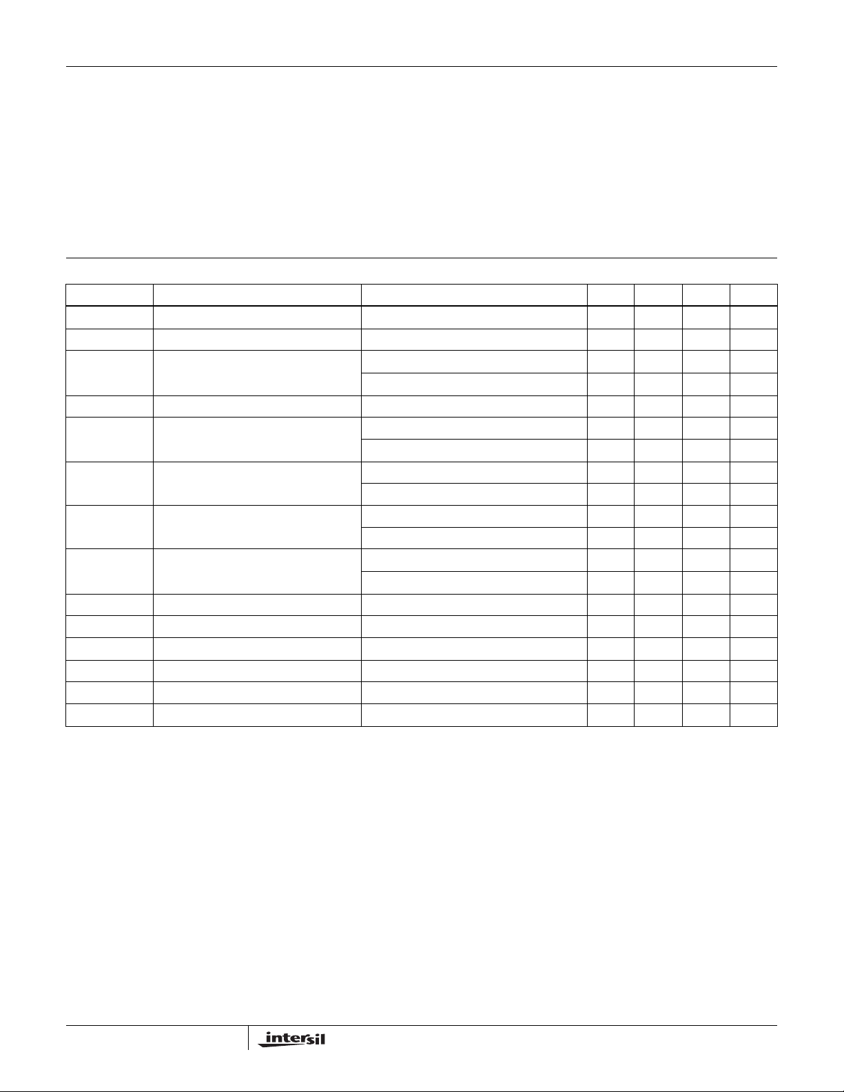
Typical Application
www.BDTIC.com/Intersil
EL7630
L1
22µH
V
IN
2.7V~5.5V
C1
1µF
OFF/ON
VDD
LX
EL7630
ENAB FB
GND
D1
R
SET
4.75Ω
FIGURE 1. TYPICAL APPLICATION CIRCUIT AND EFFICIENCY vs LED CURRENT
Typical Performance Curves
0.7
0.6
0.5
0.4
0.3
0.2
0.1
QUIESCENT CURRENT (mA)
0
0123456
V
(V)
IN
LEDs
C2
0.22µF
90
85
80
75
EFFICIENCY (%)
70
65
0 5 10 15 20 25 30
LED CURRENT (mA)
24.6
24.595
24.59
24.585
24.58
24.575
24.57
LED CURRENT (mA)
24.565
24.56
0 5 10 15 20
V
(V)
OUT
FIGURE 2. QUIESCENT CURRENT (ENABLE)
24.7
24.68
24.66
24.64
24.62
24.6
LED CURRENT (mA)
24.58
24.56
2.5 3 3.5 4 4.5 5 5.5
(V)
V
IN
FIGURE 4. LINE REGULATION FIGURE 5. SWITCHING FREQUENCY vs TEMPERATURE
3
FIGURE 3. LOAD REGULATION (V
1.34
1.32
1.3
1.28
1.26
1.24
1.22
SWITCHING FREQUENCY (MHz)
1.2
-40 10 60
TEMPERATURE (°C)
=4V)
IN
February 22, 2006
FN7371.1
Page 4

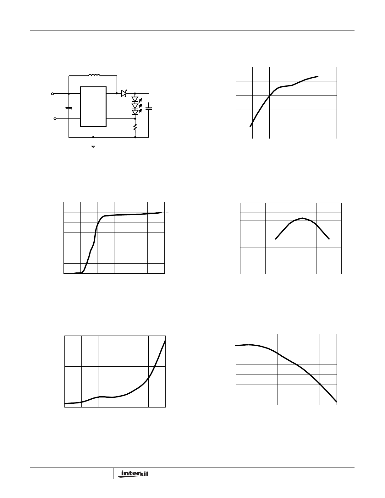
Typical Performance Curves
www.BDTIC.com/Intersil
Block Diagram
EL7630
22
20
16
12
(mA)
OUT
I
8
4
0
0 20 40 60 80 100
DUTY-CYCLE (D)
FIGURE 6. PWM DIMMING CURVE (400Hz)
Vin Enable
Vin Enable
1.2MHz Oscillator and Ramp
1.2MHz Oscillator and Ramp
Generator
Generator
PWM
PWM
Comparator
Comparator
GM Amp
GM Amp
Compensation
Compensation
(shared with PGND
(shared with PGND
in TSOT5 package)
in TSOT5 package)
FIGURE 7. EL7630 BLOCK DIAGRAM
Pin Functions
LX (Pin 1) - Switching Pin. Connect to inductor and diode.
GND (Pin 2) - Ground Pin. Connect to local ground.
FB (Pin 3) - Feedback Pin. Connect to the cathode of lowest
LED and the sense resistor.
PWM Logic
PWM Logic
Controller
Controller
GM
GM
Amplifier
Amplifier
GND
GND
EL7630
EL7630
LX
LX
FET
FET
Driver
Driver
Current
Current
Sense
Sense
PGND
PGND
FB
95mV
95mV
Bandgap
Bandgap
Reference
Reference
Generator
Generator
FB
PGND (Pin 5, SC-70 Package) - Ground Pin. Connect to
Pin 2 and to local ground.
V
(Pin5/Pin6 SC-70 Package) - Input Supply Pin.
IN
Connect to the input supply voltage.
ENAB (Pin 4) - Enable Pin. Connect to enable signal to
turn-on or off the device.
4
FN7371.1
February 22, 2006
Page 5
Detailed Description
www.BDTIC.com/Intersil
EL7630 uses a constant frequency, current mode control
scheme to provide excellent line and load regulation. It
can drive up to 6 LEDs in series or 15 LEDs in
parallel/series configuration, with efficiencies of up 86%.
EL7630 operates from an input voltage of 2.7V to 5.5V and
can boost up to 27V.
Steady-State Operation
EL7630 operates with constant frequency PWM. The
switching frequency is around 1.2MHz. Depending on the
input voltage, inductance, number of LEDs and the LED
current, the converter operates in either continuous
conduction mode or discontinuous conduction mode. Both
are normal. The forward current of the LED is set using the
R
resistor. In steady state mode, this current is given by
SET
the equation:
V
---------------=
R
FB
SET
LED
V
FB
---------------
R
SET
(EQ. 1)
D⋅=
(EQ. 2)
I
LED
Shut-Down
The ENAB pin, when taken low places EL7630 into power
down mode. When in power down, the supply current
reduced to less than 1µA.
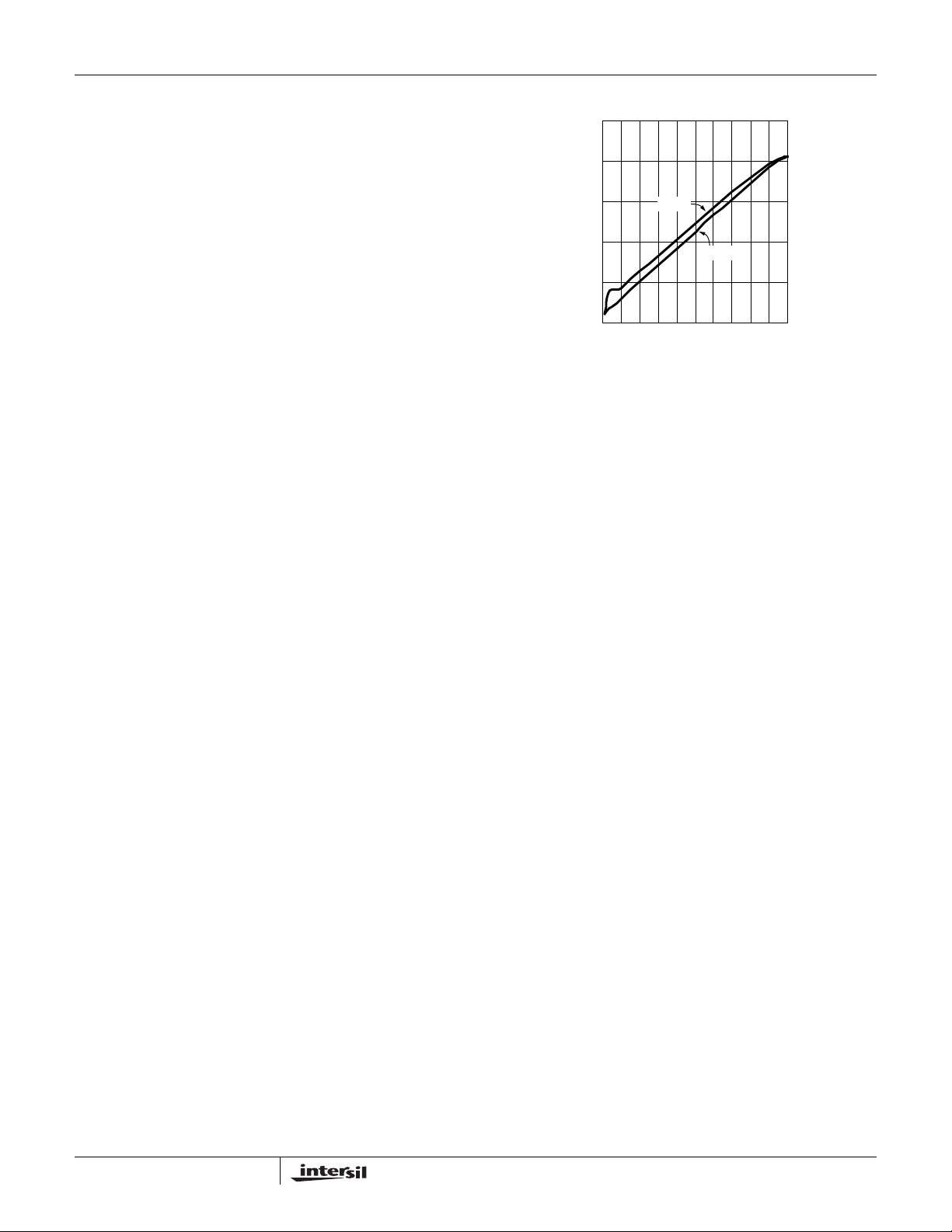
Dimming Control
The ENAB pin also doubles as a brightness control. There
are two different types of dimming control methods. The first
dimming control is controlled through the duty-cycle of the
ENAB input PWM waveform, which can operate at
frequencies of 400Hz to 1kHz. The LEDs operate at either
zero or full current. This is called PWM dimming control
method. The relationship between the average LED current
and the duty-cycle (D) of the ENAB pin’s waveform is as
follows:
average I
The magnitude of the PWM signal should be higher than the
minimum ENAB voltage high. The bench PWM dimming test
results are shown in Figure 8. In the test, two PWM
frequencies 400Hz and 1kHz are chosen to compare the
linear dimming range. It is clear that for lower PWM
frequency, the linear dimming range is wider than one for
higher PWM frequency. In the PWM dimming test, the output
capacitor is 0.22µF.
EL7630
25
20
15
(mA)
10
OUT
I
5
0
0 10203040506070809010
FIGURE 8. PWM DIMMING LINEAR RANGE (FOR 400Hz AND
1kHz PWM FREQUENCIES CONDITION,
C
OUT
1kHz
400Hz
DUTY-CYCLE (%)
= 0.22µF)
The second dimming control is to apply a variable DC
voltage to adjust the LED current. This is called analog
dimming control. The dimming control using a DC voltage is
shown in Figure 9. As the DC dimming signal voltage
increases, the voltages drop on R
the voltage drop on R
decreases. Thus, the LED current
SET
and R2 increases and
1
decreases. The DC dimming signal voltage can be a variable
DC voltage or a DC voltage generated from a PWM control
signal. For some application areas, the PWM control signal
is a high frequency signal. To make dimming controllable
with these high frequency PWM signals, the high frequency
components of the PWM control signal should be filtered to
get the equivalent DC voltage. The equivalent DC voltage is
then used as the variable DC voltage for dimming LED
current.
I
V
LED
Dim
V
FB
---------------
R
SET
R
2
-------
R
1
+
R
1R2
---------------------
R
2
R
1
⋅⋅=
V
FB
------- F–+
R
V
DimR1
---------------------------–⋅=
R
SETR2
1
2
⋅
⋅
(EQ. 3)
(EQ. 4)
where F is the brightness with respect to the undimmed
value.
5
FN7371.1
February 22, 2006
Page 6

EL7630
www.BDTIC.com/Intersil
L1
22µH
V
IN
2.7V~5.5V
C1
1µF
OFF/ON
FIGURE 9. ANALOG DIMMING CONTROL APPLICATION
For a required LED current I
and R
, the dimming DC voltage V
2
V
DimVFBVFBILED
CIRCUIT
– R
VDD
LX
LX
EL7630
ENAB FB
GND
LED
⋅()+
SET
It is clear that as the required LED current I
the rate current V
FB/RSET
, V
Dim
D1
LEDs
C2
0.22µF
R2
R1
R
SET
4.75Ω
DIMMING SIGNAL
and chosen values of R1
can be expressed as:
Dim
R
2
-------
⋅=
R
1
is closed to
LED
is closed to VFB. As the
(EQ. 5)
required LED current is lower than the rate current, the
dimming DC voltage V
is increased in R2/R1 factor.
Dim
Open-Voltage Protection
In some applications, it is possible that the output is
opened, e.g. when the LEDs are disconnected from the
circuit or the LEDs fail. In this case the feedback voltage
will be zero. The EL7630 will then switch to a high duty
cycle resulting in a high output voltage, which may cause
the LX pin voltage to exceed its maximum 27V rating. To
implement overvoltage protection, a zener diode Dz and a
resistor R
voltage on the LX pin as shown in Figure 10. It is clear that
as the zener is turned on, due to the overvoltage, the zener
diode’s current will set up a voltage on R
voltage is applied on FB pin as the feedback node. This
feedback will prevent the output from reaching the
overvoltage condition. In the overvoltage protection circuit
design, the zener voltage should be larger than the
maximum forward voltage of the LED string.
can be used at the output and FB pin to limit the
1
and R
V
IN
2.7V~5.5V
1µF
OFF/ON
C1
L1
22µH
VDD
LX
EL7630
ENAB FB
GND
D1
Dz
R1
R
SET
4.75Ω
1
SET
LEDs
and this
C2
0.22µF
Components Selection
The input capacitance is normally 0.22µF~4.7µF and the
output capacitor is 0.22µF~1µF. X5R or X7R type of ceramic
capacitor with the correct voltage rating is recommended.
The output capacitor value will affect PWM dimming
performance. For lower output capacitor values, the range of
PWM dimming is wider than for higher values of output
capacitor.
When choosing an inductor, make sure the inductor can
handle the average and peak currents given by the following
formulas (80% efficiency assumed):
I
⋅
LEDVOUT
I
LAVG
I
LPKILAVG
∆
I
Where:
• ∆I
• L inductance in H.
•f
The boost inductor can be chosen in a wide range of
inductance (10µH~82µH). For 10µH inductor value, the
boost inductor current will be in discontinuous mode. As the
inductor value decreases further, the ripple of the boost
inductor current is increased and can even trigger
overcurrent protection. For high boost inductor value, the
boost inductor current will be in continuous mode. For
general boost converter, as the converter operates in
continuous mode, there is right half plane zero (RHPZ). If
RHPZ frequency is less than or close to the control loop
crossover frequency, there is a stability issue. In EL7630, the
compensation network is well designed and there is no
RHPZ stability issue even if the inductor value is over 82µH.
For the same series of inductors, a lower inductance has
lower DC resistance (DCR), which causes less conducting
loss, but higher peak to peak current variation, which
generates more RMS current loss. Figure 11 shows the
efficiency of the demo board with different LED load for a
specific series of inductor.
The diode used should be a schottky type with minimum
reverse voltage of 28V. The diode’s peak current is the same
as the inductor’s peak current. The schottky RMS current is:
I
RMS
---------------------------------=
⋅
0.8 V
IN
1
-- -
∆⋅+=
I
L
2
V
INVOUTVIN
---------------------------------------------------=
L
LV
⋅⋅
is the peak-to-peak inductor current ripple in Ampere
L
switching frequency, typically 1.2MHz
OSC
D2I
–()⋅
OUTfOSC
2
⋅
⋅=
LAVG
2
1
-- -
∆⋅+
I
L
6
(EQ. 6)
(EQ. 7)
(EQ. 8)
(EQ. 9)
FIGURE 10. LED DRIVER WITH OVERVOLTAGE
PROTECTION CIRCUIT
6
FN7371.1
February 22, 2006
Page 7

EL7630
www.BDTIC.com/Intersil
The efficiency bench test results are shown in Figure 11. In
the test, the input voltage is 4V and 2, 3, 4, 5 and 6 LEDs are
used as the load (boost inductor L = 22µH Sumida
CDRH5D28R-220NC).
90
22µH,VIN=4V
85
80
75
70
65
EFFICIENCY (%)
60
55
0102030
FIGURE 11. EFFICIENCY CURVE WITH 2, 3, 4, 5 AND 6 LEDs
LOAD
4LED
6LED
3LED
LED CURRENT (mA)
2LED
5LED
White LED Connections
One leg of LEDs connected in series will ensure brightness
uniformity. The 27V maximum output voltage specification
enables up to 6 LEDs to be placed in series.
In order to output more power to drive more LEDs, LEDs
should be in series/parallel connection. Due to the LED's
negative temperature coefficient, in each parallel branch, the
driving source should be high impedance, to balance the
LED current in each branch. One of the ways to ensure the
brightness uniformity is to add mirror current balance circuit,
built up with three transistors for the 15 LEDs series/parallel
connection application shown in Figure 12.
PCB Layout Considerations
The PCB layout is very important for the converter to
function properly. For the SC-70 6 pin package, Power
Ground and Signal Ground should be separated to ensure
the high pulse current in the power ground does not interfere
with the sensitive signals connected to Signal Ground. Both
grounds should only be connected at one point right at the
chip. The heavy current loops (V
L1-D1-C2-PGND) should be as short as possible. For the
TSOT 5 pin package, there is no separated GND. All return
GNDs should be connected in GND pin but with no sharing
branch. Based on the signal level on each branch, the lower
power level of the branch, the closer the branch to GND pin
in order to minimize the branch interactive.
The FB
R
pin is most important. The current sense resistor
should be very close to this pin. If a long trace is
SET
required to the LEDs, a small decoupling capacitor should be
placed at this pin.
The heat of the IC is mainly dissipated through the PGND
pin. Maximizing the copper area connected to this pin is
preferable. In addition, a solid ground plane is always helpful
for the EMI performance.
The demo board is a good example of layout based on the
principle. Please refer to the EL7630 Application Brief for the
layout.
-L1-LX-PGND, and VIN-
IN
D1
D1
L1
L1
V
IN
2.7V~5.5V
C1
OFF/ON
FIGURE 12. LEDs IN SERIES/PARALLEL WITH MIRROR
VDD
VDD
LX
LX
EL7630
EL7630
ENAB FB
ENAB FB
GND
GND
CURRENT BALANCE
R
SET
C2
LEDs
All Intersil U.S. products are manufactured, assembled and tested utilizing ISO9000 quality systems.
Intersil Corporation’s quality certifications can be viewed at www.intersil.com/design/quality
Intersil products are sold by description only. Intersil Corporation reserves the right to make changes in circuit design, software and/or specifications at any time without
notice. Accordingly, the reader is cautioned to verify that data sheets are current before placing orders. Information furnished by Intersil is believed to be accurate and
reliable. However, no responsibility is assumed by Intersil or its subsidiaries for its use; nor for any infringements of patents or other rights of third parties which may result
from its use. No license is granted by implication or otherwise under any patent or patent rights of Intersil or its subsidiaries.
For information regarding Intersil Corporation and its products, see www.intersil.com
7
FN7371.1
February 22, 2006
 Loading...