


S
N
G
®
O
F
D
E
D
N
E
R
T
O
N
S
E
M
M
O
C
7
L
E
Data Sheet May 9, 2005
E
E
W
E
N
R
4
5
5
I
S
E
D
EL7564
FN7297.3
Monolithic 4 Amp DC/DC Step-Down
Regulator
The EL7564 is an integrated, full-featured synchronous stepdown regulator with output voltage adjustable from 1.0V to
3.8V. It is capable of delivering 4A continuous current at up
to 95% efficiency. The EL7564 operates at a constant
frequency pulse width modulation (PWM) mode, making
external synchronization possible. Patented on-chip
resistorless current sensing enables current mode control,
which provides cycle-by-cycle current limiting, over-current
protection, and excellent step load response. The EL7564
features power tracking, which makes the start-up
sequencing of multiple converters possible. A junction
temperature indicator conveniently monitors the silicon die
temperature, saving the designer time on the tedious
thermal characterization. The minimal external components
and full functionality make this EL7564 ideal for desktop and
portable applications.
The EL7564 is specified for operation over the -40°C to
+85°C temperature range.
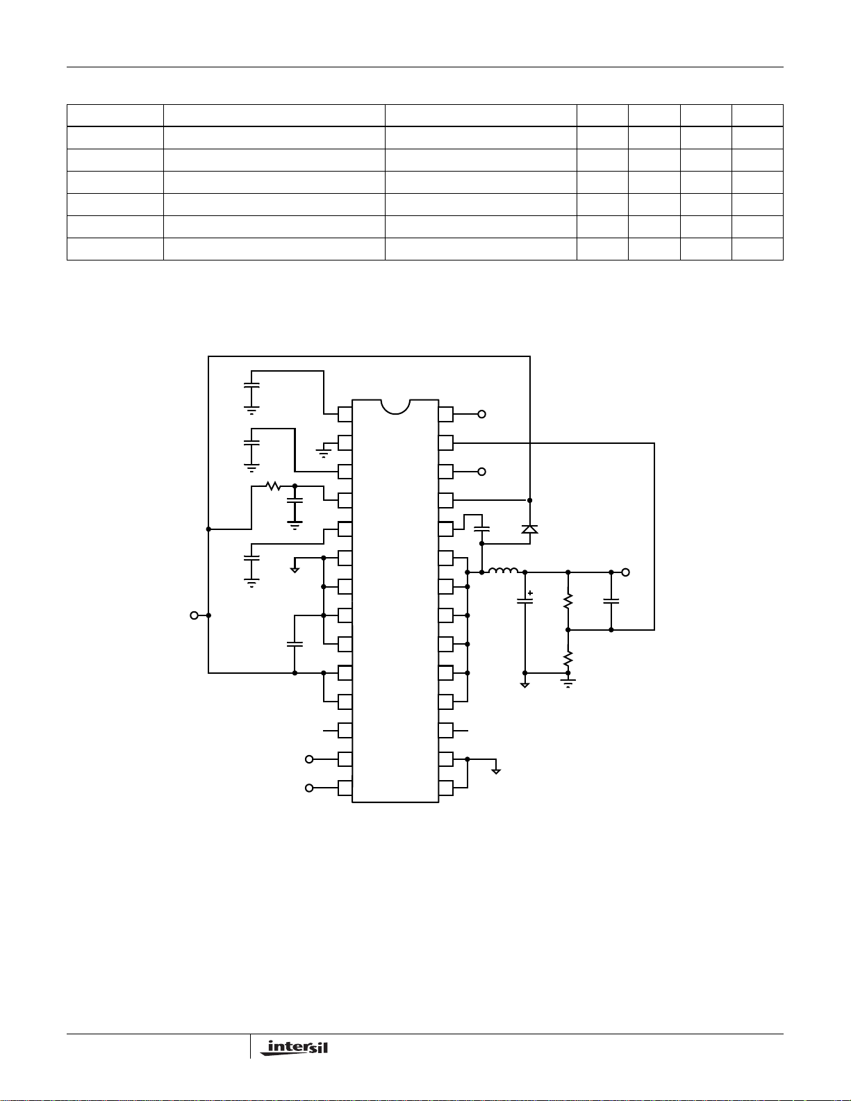
Typical Application Diagrams
EL7564
[20-PIN SO (0.300”)]
TOP VIEW
C5
0.1µF
1
VREF
C4
390pF
R4
C3
22Ω
0.22µF
C2
2.2nF
V
IN
5V
C1
330µF
2
3
4
5
6
7
8
9
10
SGND
COSC
VDD
VTJ
PGND
PGND
VIN
STP
STN
EN
FB
PG
VDRV
VHI
LX
LX
PGND
PGND
PGND
20
19
18
17
16
15
14
13
12
11
C6
0.22µF
L1
4.7µH
330µF
C7
D1
3.3V, 4A
R2
2.37kΩ
R1
1kΩ
V
OUT
C10
100pF
Features
• Integrated synchronous MOSFETs and current mode
controller
• 4A continuous output current
• Up to 95% efficiency
• 4.5V to 5.5V input voltage
• Adjustable output from 1V to 3.8V
• Cycle-by-cycle current limit
• Precision reference
• ±0.5% load and line regulation
• Adjustable switching frequency to 1MHz
• Oscillator synchronization possible
• Internal soft start
• Over voltage protection
• Junction temperature indicator
• Over temperature protection
• Under voltage lockout
• Multiple supply start-up tracking
• Power good indicator
• 20-pin SO (0.300”) package
• 28-pin HTSSOP package
• Pb-Free available (RoHS compliant)
Applications
• DSP, CPU core and IO supplies
• Logic/Bus supplies
• Portable equipment
• DC/DC converter modules
• GTL + Bus power supply
Typical Application Diagrams continued on page 3
Manufactured Under U.S. Patent No. 5,7323,974
1
CAUTION: These devices are sensitive to electrostatic discharge; follow proper IC Handling Procedures.
1-888-INTERSIL or 1-888-352-6832
| Intersil (and design) is a registered trademark of Intersil Americas Inc.
Copyright Intersil Americas Inc. 2003, 2005. All Rights Reserved
All other trademarks mentioned are the property of their respective owners.
Ordering Information
EL7564
TAPE &
PART NUMBER PACKAGE
EL7564CM 20-Pin SO (0.300”) - MDP0027
EL7564CM-T13 20-Pin SO (0.300”) 13” MDP0027
EL7564CMZ
(See Note)
EL7564CMZ-T13
(See Note)
EL7564CRE 28-Pin HTSSOP - MDP0048
EL7564CRE-T7 28-Pin HTSSOP 7” MDP0048
EL7564CRE-T13 28-Pin HTSSOP 13” MDP0048
EL7564CREZ
(See Note)
EL7564CREZ-T7
(See Note)
EL7564CREZ-T13
(See Note)
NOTE: Intersil Pb-free products employ special Pb-free material sets;
molding compounds/die attach materials and 100% matte tin plate
termination finish, which are RoHS compliant and compatible with
both SnPb and Pb-free soldering operations. Intersil Pb-free products
are MSL classified at Pb-free peak reflow temperatures that meet or
exceed the Pb-free requirements of IPC/JEDEC J STD-020.
20-Pin SO (0.300”)
(Pb-free)
20-Pin SO (0.300”)
(Pb-free)
28-Pin HTSSOP
(Pb-free)
28-Pin HTSSOP
(Pb-free)
28-Pin HTSSOP
(Pb-free)
REEL
13” MDP0027
7” MDP0048
13” MDP0048
PKG. DWG.
#
- MDP0027
- MDP0048
2
FN7297.3
May 9, 2005
EL7564
Absolute Maximum Ratings (T
Supply Voltage between V
V
Voltage . . . . . . . . . . . . . . . . . . . . . . . . . . . . . . . . . . . .VIN +0.3V
LX
Input Voltage . . . . . . . . . . . . . . . . . . . . . . . . GND -0.3V, V
V
Voltage . . . . . . . . . . . . . . . . . . . . . . . . . . GND -0.3V, V
HI
CAUTION: Stresses above those listed in “Absolute Maximum Ratings” may cause permanent damage to the device. This is a stress only rating and operation of the
device at these or any other conditions above those indicated in the operational sections of this specification is not implied.
IMPORTANT NOTE: All parameters having Min/Max specifications are guaranteed. Typical values are for information purposes only. Unless otherwise noted, all tests
are at the specified temperature and are pulsed tests, therefore: TJ = TC = T
or VDD and GND . . . . . . . . . . . . +6.5V
IN
DC Electrical Specifications V
= 25°C)
A
DD
DD
LX
= V
= 5V, TA = TJ = 25°C, C
IN
+0.3V
+6.5V
Storage Temperature . . . . . . . . . . . . . . . . . . . . . . . . -65°C to +150°C
Operating Ambient Temperature . . . . . . . . . . . . . . . . -40°C to +85°C
Operating Junction Temperature . . . . . . . . . . . . . . . . . . . . . . . +135°
A
= 1.2nF, Unless Otherwise Specified.
OSC
PARAMETER DESCRIPTION CONDITIONS MIN TYP MAX UNIT
V
REF
V
REFTC
V
REFLOAD
V
RAMP
I
OSC_CHG
I
OSC_DIS
I
VDD+VDRV
IVDD_OFF V
V
DD_OFF
V
DD_ON
T
OT
T
HYS
I
LEAK
I
LMAX
R
DSON
R
DSONTC
I
STP
I
STN
Reference Accuracy 1.24 1.26 1.28 V
Reference Temperature Coefficient 50 ppm/°C
Reference Load Regulation 0 < I
< 50µA -1 %
REF
Oscillator Ramp Amplitude 1.15 V
Oscillator Charge Current 0.1V < V
Oscillator Discharge Current 0.1V < V
VDD+V
DD
Supply Current VEN = 4V, F
DRV
Standby Current EN = 0 1 1.5 mA
< 1.25V 200 µA
OSC
< 1.25V 8 mA
OSC
= 120kHz 2 3.5 5 mA
OSC
VDD for Shutdown 3.5 3.9 V
VDD for Startup 44.35V
Over Temperature Threshold 135 °C
Over Temperature Hysteresis 20 °C
Internal FET Leakage Current EN = 0, LX = 5V (low FET), LX = 0V (high FET) 10 µA
Peak Current Limit 5 A
FET On Resistance Wafer level test only 30 60 mΩ
R
Tem p c o 0.2 mΩ/°C
DSON
Auxiliary Supply Tracking Positive
Input Pull Down Current
Auxiliary Supply Tracking Negative
V
V
STP
STN
= V
/ 2 -4 2.5 µA
IN
= V
/ 2 2.5 4 µA
IN
Input Pull Up Current
V
PGP
V
PGN
V
PG_HI
V
PG_LO
V
OVP
V
FB
Positive Power Good Threshold With respect to target output voltage 6 14 %
Negative Power Good Threshold With respect to target output voltage -14 -6 %
Power Good Drive High I
= +1mA 4 V
PG
Power Good Drive Low IPG = -1mA 0.5 V
Over Voltage Protection 10 %
Output Initial Accuracy (EL7564CM) I
Output Initial Accuracy
= 0A 0.960 0.975 0.99 V
LOAD
0.977 0.992 1.007 V
(EL7564CRE)
V
FB_LINE
V
FB_LOAD
V
FB_TC
I
FB
V
EN_HI
V
EN_LO
I
EN
Output Line Regulation V
Output Load Regulation 0.5A < I
Output Temperature Stability -40°C < TA < 85°C, I
Feedback Input Pull Up Current V
= 5V, ∆VIN = 10%, I
IN
< 4A 0.5 %
LOAD
LOAD
= 0V 100 200 nA
FB
= 0A 0.5 %
LOAD
= 2A ±1 %
EN Input High Level 3.2 4 V
EN Input Low Level 1 V
Enable Pull Up Current VEN = 0 -4 -2.5 µA
3
FN7297.3
May 9, 2005
EL7564
Closed-Loop AC Electrical Specifications V
= V
= 5V, TA = TJ = 25°C, C
S
IN
= 1.2nF, Unless Otherwise Specified.
OSC
PARAMETER DESCRIPTION CONDITIONS MIN TYP MAX UNIT
F
OSC
t
SYNC
M
SS
t
BRM
t
LEB
D
MAX
Oscillator Initial Accuracy 105 117 130 kHz
Minimum Oscillator Sync Width 25 ns
Soft Start Slope 0.5 V/ms
FET Break Before Make Delay 15 ns
High Side FET Minimum On Time 150 ns
Maximum Duty Cycle 95 %
Typical Application Diagrams (Continued)
EL7654
(28-PIN HTSSOP)
TOP VIEW
C5
0.1µF
1
VREF
C4
390pF
R4
22Ω
C2
2.2nF
V
IN
5V
C3
0.22µF
2
3
4
5
6
7
8
SGND
COSC
VDD
VTJ
PGND
PGND
PGND
EN
FB
PG
VDRV
VHI
LX
LX
LX
28
27
26
25
24
23
22
21
C6 D1
0.22µF
L1
4.7µH
C7 R2 C10
330µF
2.37kΩ
V
OUT
3.3V, 4A
100pF
PGND
330µF
9
VIN
10
11
VIN
12
NC
STP
13
STN
4
LX
LX
LX
NC
PGND
PGND
20
19
18
17
16
1514
R1
1kΩ
FN7297.3
May 9, 2005
Pin Descriptions
EL7564
20-PIN SO
(0.300”)
28-PIN
HTSSOP PIN NAME PIN FUNCTION
1 1 VREF Bandgap reference bypass capacitor; typically 0.1µF to SGND
2 2 SGND Control circuit negative supply or signal ground
3 3 COSC Oscillator timing capacitor (see performance curves)
4 4 VDD Control circuit positive supply; normally connected to VIN through an RC filter
5 5 VTJ Junction temperature monitor; connected with 2.2nF to 3.3nF to SGND
6, 7 6, 7, 8, 9 PGND Ground return of the regulator; connected to the source of the low-side synchronous NMOS
power FET
8 10, 11 VIN Power supply input of the regulator; connected to the drain of the high-side NMOS power FET
9 13 STP Auxiliary supply tracking positive input; tied to regulator output to synchronize start up with a
second supply; leave open for stand alone operation; 2µA internal pull down current
10 14 STN Auxiliary supply tracking negative input; connect to output of a second supply to synchronize
start up; leave open for stand alone operation; 2µA internal pull up current
11, 12, 13 15, 16 PGND Ground return of the regulator; connected to the source of the low-side synchronous NMOS
power FET
14, 15 18, 19, 20, 21,
22, 23
LX Inductor drive pin; high current output whose average voltage equals the regulator output
voltage
16 24 VHI Positive supply of high-side driver; boot strapped from VDRV to LX with an external 0.22µF
capacitor
17 25 VDRV Positive supply of low-side driver and input voltage for high side boot strap
18 26 PG Power good window comparator output; logic 1 when regulator output is within ±10% of target
output voltage
19 27 FB Voltage feedback input; connected to external resistor divider between VOUT and SGND; a
125nA pull-up current forces VOUT to SGND in the event that FB is floating
20 28 EN Chip enable, active high; a 2µA internal pull up current enables the device if the pin is left open;
a capacitor can be added at this pin to delay the start of converter
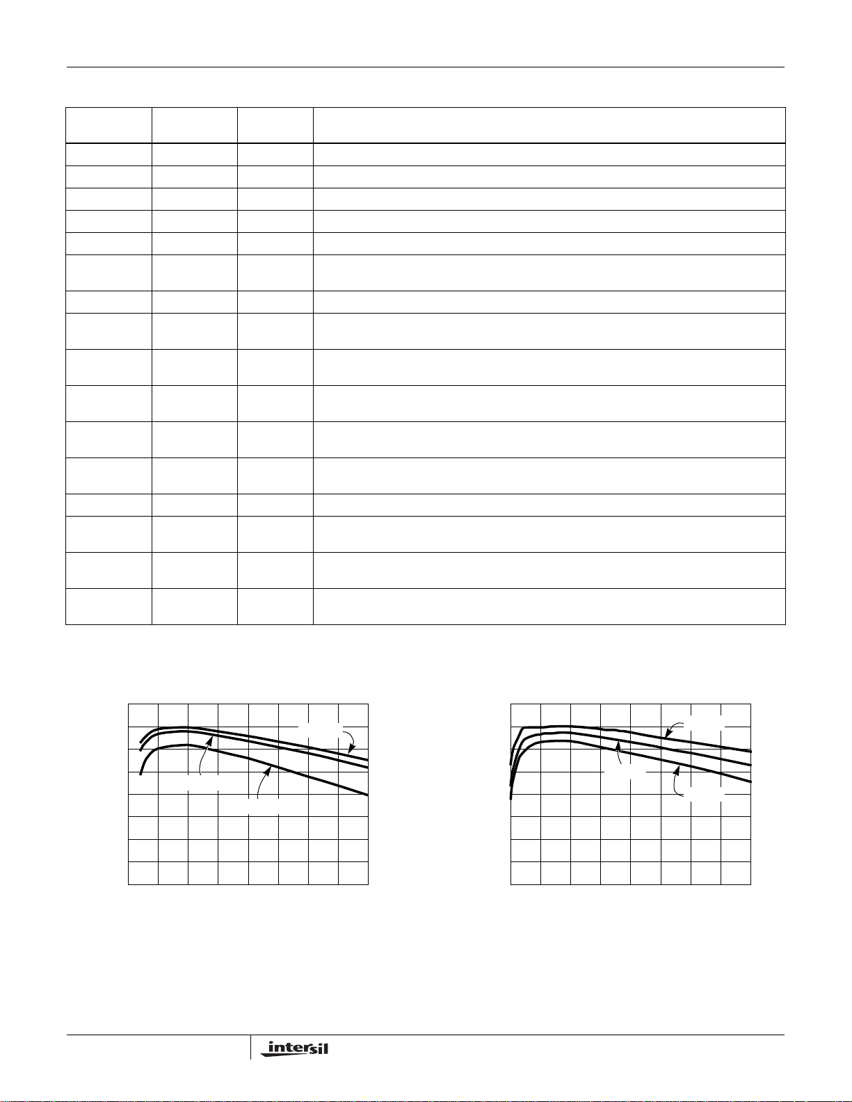
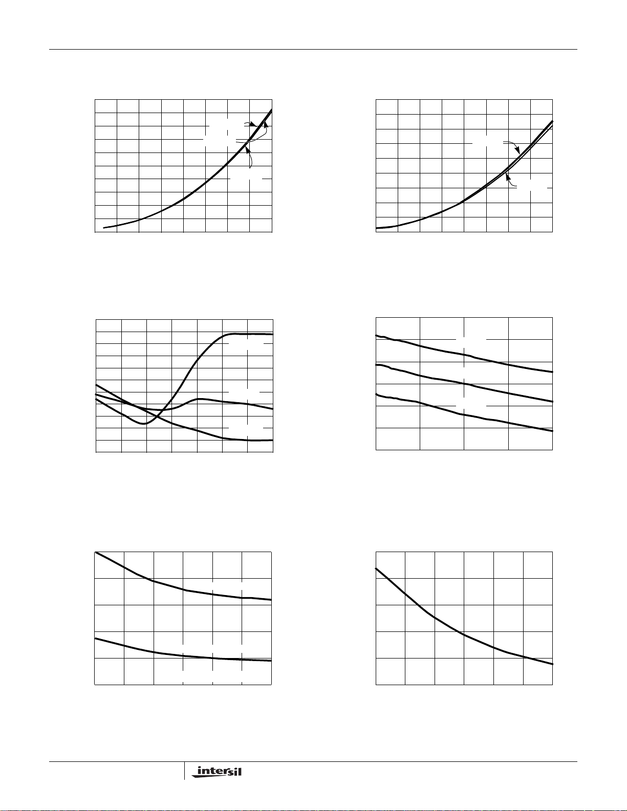
Typical Performance Curves
VIN=5V
100
95
90
85
80
75
EFFICIENCY (%)
70
65
60
043.532.5210.5 1.5
FIGURE 1. EL7564CM EFFICIENCY FIGURE 2. EL7564CRE EFFICIENCY
VO=2.8V
VO=1.8V
LOAD CURRENT I
5
O
(A)
VO=3.3V
VIN=5V
100
95
90
85
80
75
EFFICIENCY (%)
70
65
60
0.1 0.6 1.1 1.6 2.1 2.6 3.1 3.6 4.1
VO=2.5V
(A)
I
O
VO=3.3V
VO=1.8V
FN7297.3
May 9, 2005
EL7564
Typical Performance Curves (Continued)
VIN=5V
2
1.6
1.2
0.8
POWER LOSS (W)
0.4
0
043.532.5210.5 1.5
OUTPUT CURRENT I
VO=3.3V
VO=2.8V
(A)
O
VO=1.8V
FIGURE 3. EL7564CM TOTAL CONVERTER POWER LOSS FIGURE 4. EL7564CRE TOTAL CONVERTER POWER LOSS
1.8
1.6
1.4
I
O
VO=3.3V
(A)
1.2
1
(W)
0.8
LOSS
P
0.6
0.4
0.2
0
00.511.522.533.54
VO=1.8V
=3.3V
V
O
3.325
3.315
3.305
3.295
OUTPUT VOLTAGE (V)
3.285
3.275
0.5 43.532.51.512
LOAD CURRENT I
VIN=5.5V
VIN=5V
VIN=4.5V
(A)
O
VO=3.3V
1.5
1
0.5
0
(V) (%)
O
V
-0.5
-1
-1.5
01234
VIN=4.5V
VIN=5V
VIN=5.5V
I
(A)
O
FIGURE 5. EL7564CM LOAD REGULATION FIGURE 6. EL7564CRE LOAD REGULATION
CONDITION:
EL7564RE THERMAL PAD SOLDERED TO 2-LAYER
TEST CONDITION:
CHIP IN THE CENTER OF COPPER AREA
50
46
42
38
34
THERMAL RESISTANCE (°C/W)
30
141.5 2.5 3.5
PCB COPPER HEAT-SINKING AREA (in
FIGURE 7. EL7564CM θ
WITH 100 LFPM AIRFLOW
1 OZ. COPPER PCB USED
23
JA
WITH NO AIRFLOW
2
)
vs COPPER AREA FIGURE 8. EL7564CRE THERMAL RESISTANCE vs PCB
PCB WITH 0.039” THICKNESS AND 1 OZ. COPPER
ON BOTH SIDES
50
45
40
(°C/W)
JA
35
θ
30
25
11.5 33.54
22.5
PCB AREA (in
2
AREA - NO AIRFLOW
)
6
FN7297.3
May 9, 2005
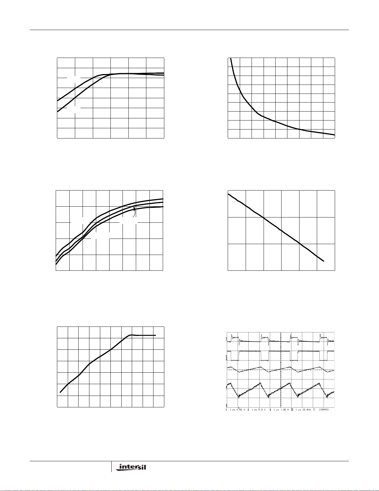
Typical Performance Curves (Continued)
EL7564
360
350
OSCILLATOR FREQUENCY (kHz)
340
330
320
310
300
290
280
IO=4A
IO=0A
-40 80-20 204060
0
TEMPERATURE (°C)
1000
900
800
700
600
(kHz)
500
S
F
400
300
200
100
100 1000200 400 600 800
(pF)
C
OSC
FIGURE 9. OSCILLATOR FREQUENCY vs TEMPERATURE FIGURE 10. SWITCHING FREQUENCY vs C
(A)
LMT
I
8
7
6
5
VIN=5.5V VIN=5V
VIN=4.5V
1.5
1.3
VTJ
1.1
900300 500 700
OSC
4
3
-40 120-20 40 100
0806020
T
(°C)
J
FIGURE 11. CURRENT LIMIT vs T
1.27
1.268
1.266
1.264
(V)
REF
1.262
V
1.26
1.258
1.256
-50 150-10 30 70 110
DIE TEMPERATURE (°C)
FIGURE 13. V
vs DIE TEMPERATURE FIGURE 14. SWITCHING WAVEFORMS
REF
0.9
015025
JUNCTION TEMPERATURE (°C)
J
FIGURE 12. VTJ vs JUNCTION TEMPERATURE
VIN=5V, VO=3.3V, IO=4A
∆V
IN
V
LX
i
L
∆V
O
12550 75 100
7
FN7297.3
May 9, 2005
Typical Performance Curves (Continued)
EL7564
VIN=5V, VO=3.3V, IO=0.2A-4A
I
O
∆V
O
VIN=5V, VO=3.3V, IO=2A
V
IN
V
O
FIGURE 15. TRANSIENT RESPONSE FIGURE 16. POWER-UP
VIN=5V, VO=3.3V, IO=4A
V
IN
V
O
VIN=5V, VO=3.3V, IO=2A
EN
FIGURE 17. POWER-DOWN FIGURE 18. RELEASING EN
VIN=5V, VO=3.3V, IO=4A
EN
V
O
FIGURE 19. SHUT-DOWN FIGURE 20. SHORT-CIRCUIT PROTECTION
V
V
I
O
O
O
VIN=5V
8
FN7297.3
May 9, 2005

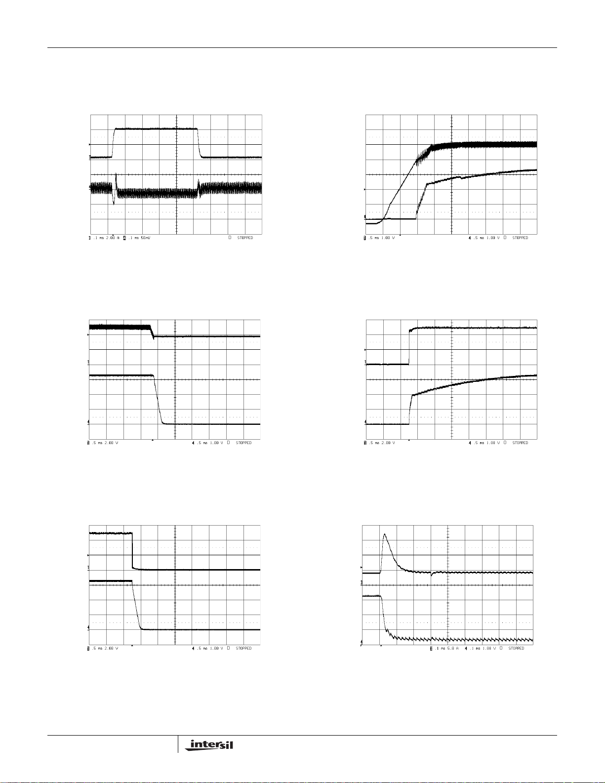
Typical Performance Curves (Continued)
JEDEC JESD51-7 HIGH EFFECTIVE THERMAL
CONDUCTIVITY TEST BOARD. HTSSOP EXPOSED
DIEPAD SOLDERED TO PCB PER JESD51-5
3.5
3.333W
3
2.5
2
1.5
1
POWER DISSIPATION (W)
0.5
0
0 255075100 150
HT
S
θ
S
J
A
O
=
P
3
2
0
8
°
C/
W
AMBIENT TEMPERATURE (°C)
12585
EL7564
JEDEC JESD51-3 LOW EFFECTIVE THERMAL
CONDUCTIVITY TEST BOARD
1
0.9
909mW
0.8
0.7
0.6
0.5
0.4
0.3
0.2
POWER DISSIPATION (W)
0.1
0
0 25 50 75 100 150
H
T
θ
S
S
J
A
O
=
P
1
1
2
0
8
°
C
/
W
85
AMBIENT TEMPERATURE (°C)
125
FIGURE 21. PACKAGE POWER DISSIPATION vs AMBIENT
TEMPERATURE
Block Diagram
V
V
EN
2.2nF
22Ω
0.22µF
TJ
V
DD
JUNCTION
TEMPERATURE
CONTROLLER
SUPPLY
VOLTAGE
REFERENCE
PWM
CONTROLLER
REF
C
OSC
OSCILLATOR
DRIVERS
FIGURE 22. PACKAGE POWER DISSIPATION vs AMBIENT
TEMPERATURE
390pF0.1µF
V
DRV
V
HI
V
IN
PGND
0.22µF
4.7µH
D
1
330µF
2370Ω
1kΩ
100pF
POWER
FET
POWER
FET
V
OUT
STP
STN
POWER
TRACKING
SGND
9
FB
V
REF
CURRENT
SENSE
-
+
PG
FN7297.3
May 9, 2005

EL7564
Applications Information
Circuit Description
General
The EL7564 is a fixed frequency, current mode controlled
DC/DC converter with integrated N-channel power
MOSFETs and a high precision reference. The device
incorporates all the active circuitry required to implement a
cost effective, user-programmable 4A synchronous stepdown regulator suitable for use in DSP core power supplies.
By combining fused-lead packaging technology with an
efficient synchronous switching architecture, high power
output (13W) can be realized without the use of discrete
external heat sinks.
Theory of Operation
The EL7564 is composed of seven major blocks:
1. PWM Controller
2. NMOS Power FETs and Drive Circuitry
3. Bandgap Reference
4. Oscillator
5. Temperature Sensor
6. Power Good and Power On Reset
7. Auxiliary Supply Tracking
PWM Controller
The EL7564 regulates output voltage through the use of
current-mode controlled pulse width modulation. The three
main elements in a PWM controller are the feedback loop
and reference, a pulse width modulator whose duty cycle is
controlled by the feedback error signal, and a filter which
averages the logic level modulator output. In a step-down
(buck) converter, the feedback loop forces the timeaveraged output of the modulator to equal the desired output
voltage. Unlike pure voltage-mode control systems, currentmode control utilizes dual feedback loops to provide both
output voltage and inductor current information to the
controller. The voltage loop minimizes DC and transient
errors in the output voltage by adjusting the PWM duty-cycle
in response to changes in line or load conditions. Since the
output voltage is equal to the time-averaged of the modulator
output, the relatively large LC time constant found in power
supply applications generally results in low bandwidth and
poor transient response. By directly monitoring changes in
inductor current via a series sense resistor the controller's
response time is not entirely limited by the output LC filter
and can react more quickly to changes in line and load
conditions. This feed-forward characteristic also simplifies
AC loop compensation since it adds a zero to the overall
loop response. Through proper selection of the currentfeedback to voltage-feedback ratio the overall loop response
will approach a one-pole system. The resulting system offers
several advantages over traditional voltage control systems,
including simpler loop compensation, pulse by pulse current
limiting, rapid response to line variation and good load step
response.
The heart of the controller is an input direct summing
comparator which sum voltage feedback, current feedback,
slope compensation ramp and power tracking signals
together. Slope compensation is required to prevent system
instability that occurs in current-mode topologies operating
at duty-cycles greater than 50% and is also used to define
the open-loop gain of the overall system. The slope
compensation is fixed internally and optimized for 500mA
inductor ripple current. The power tracking will not contribute
any input to the comparator steady-state operation. Current
feedback is measured by the patented sensing scheme that
senses the inductor current flowing through the high-side
switch whenever it is conducting. At the beginning of each
oscillator period the high-side NMOS switch is turned on.
The comparator inputs are gated off for a minimum period of
time of about 150ns (LEB) after the high-side switch is
turned on to allow the system to settle. The Leading Edge
Blanking (LEB) period prevents the detection of erroneous
voltages at the comparator inputs due to switching noise. If
the inductor current exceeds the maximum current limit
(I
) a secondary over-current comparator will terminate
LMAX
the high-side switch on time. If I
has not been reached,
LMAX
the feedback voltage FB derived from the regulator output
voltage V
is then compared to the internal feedback
OUT
reference voltage. The resultant error voltage is summed
with the current feedback and slope compensation ramp.
The high-side switch remains on until all four comparator
inputs have summed to zero, at which time the high-side
switch is turned off and the low-side switch is turned on.
However, the maximum on-duty ratio of the high-side switch
is limited to 95%. In order to eliminate cross-conduction of
the high-side and low-side switches a 15ns break-beforemake delay is incorporated in the switch drive circuitry. The
output enable (EN) input allows the regulator output to be
disabled by an external logic control signal.
Output Voltage Setting
In general, EL7564CM:
R
V
OUT
0.975V 1
and EL7564CRE:
OUT
0.992V 1
V
A 100nA pull-up current from FB to V
GND in the event that FB is floating.
2
-------+
×=
R
1
R
2
-------+
×=
R
1
forces V
DD
OUT
to
10
FN7297.3
May 9, 2005
EL7564
NMOS Power FETs and Drive Circuitry
The EL7564 integrates low on-resistance (30mΩ) NMOS
FETs to achieve high efficiency at 4A. In order to use an
NMOS switch for the high-side drive it is necessary to drive
the gate voltage above the source voltage (L
accomplished by bootstrapping the V
voltage with an external capacitor C
HI
VHI
). This is
X
pin above the LX
and internal switch
and diode. When the low-side switch is turned on and the
L
voltage is close to GND potential, capacitor C
X
charged through an internal switch to V
DRV
, typically 5V. At
VHI
is
the beginning of the next cycle the high-side switch turns
on and the L
As the L
follows and eventually reaches a value of V
typically 10V, for V
pins begin to rise from GND to VIN potential.
X
pin rises the positive plate of capacitor C
X
= VIN = 5V. This voltage is then
DRV
DRV
VHI
+ VIN,
level shifted and used to drive the gate of the high-side
FET, via the V
pin. A value of 0.22µF for C
HI
VHI
is
recommended.
Reference
A 1.5% temperature compensated bandgap reference is
integrated in the EL7564. The external V
capacitor acts
REF
as the dominant pole of the amplifier and can be increased
in size to maximize transient noise rejection. A value of
0.1µF is recommended.
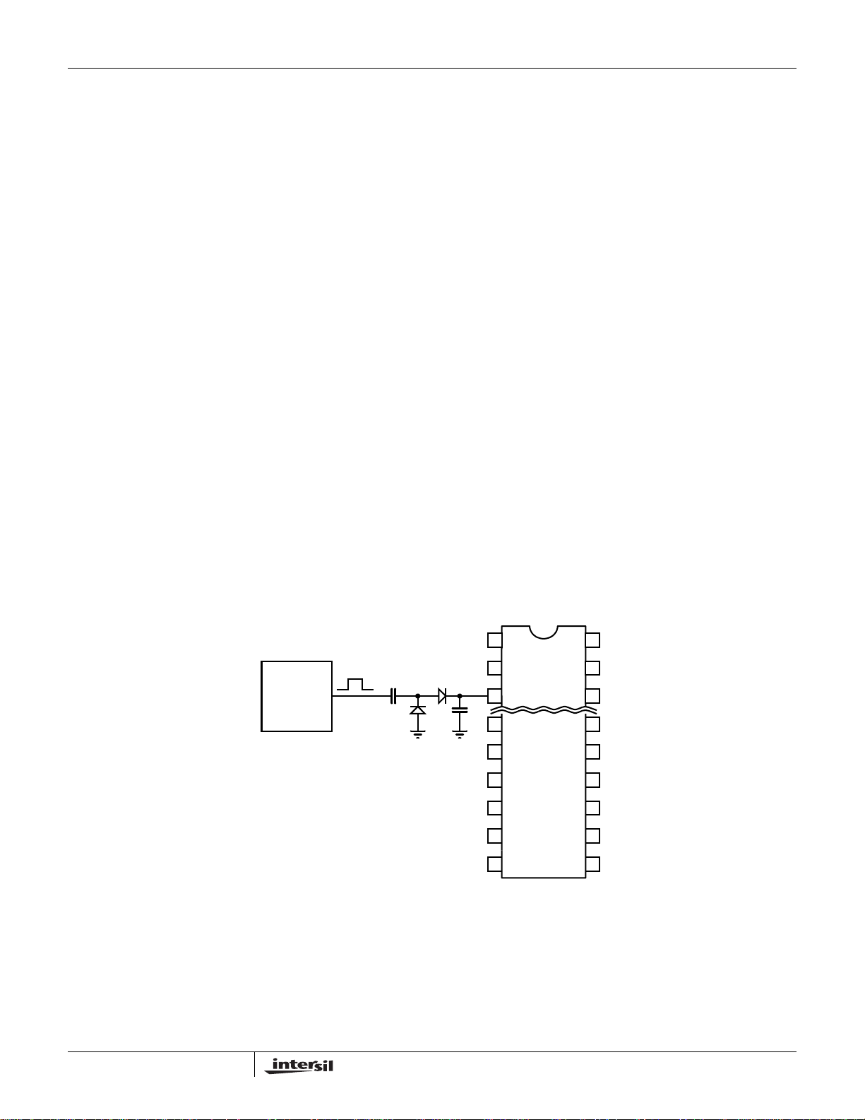
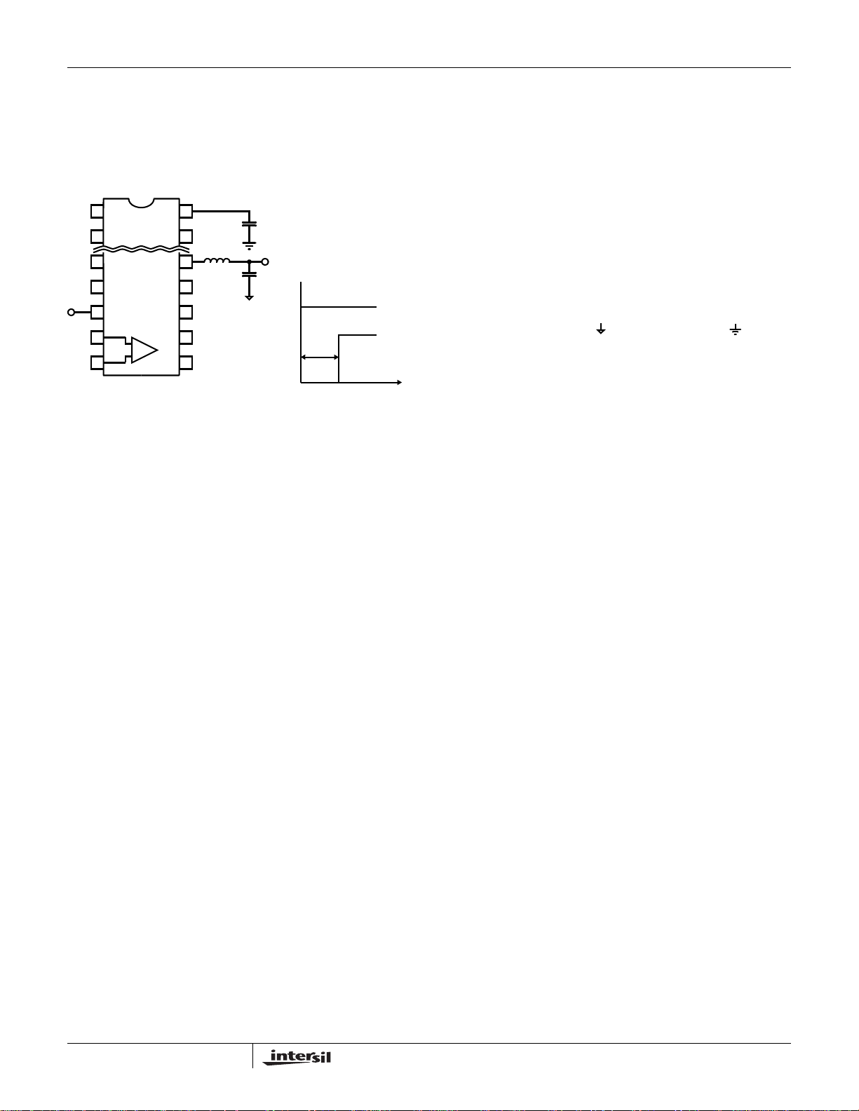
Oscillator
The system clock is generated by an internal relaxation
oscillator with a maximum duty-cycle of approximately 95%.
Operating frequency can be adjusted through C
OSC
.
When external synchronization is required, always choose
C
such that the free-running frequency is at least 20%
OSC
lower than that of the sync source to accommodate
component and temperature variations. Figure 21 shows a
typical connection.
Junction Temperature Sensor
An internal temperature sensor continuously monitors die
temperature. In the event that the die temperature exceeds
the thermal trip-point, the system is in a fault state and will
be shut down. The upper and low trip-points are set to 135°C
and 115°C respectively.
The V
pin is an accurate indication of the internal silicon
TJ
junction temperature (see performance curve.) The junction
temperature T
(°C) can be determined from the following
J
relation:
TJ75
Where V
1.2 VTJ–
-------------------------+=
0.00384
is the voltage at the VTJ pin in volts.
TJ
Power Good and Power On Reset
During power up the output regulator will be disabled until
V
reaches a value of approximately 4V. About 500mV
IN
hysteresis is present to eliminate noise-induced oscillations.
Under-voltage and over-voltage conditions on the regulator
output are detected through an internal window comparator.
A logic high on the PG output indicates that the regulated
output voltage is within about +10% of the nominal selected
EXTERNAL
OSCILLATOR
FIGURE 23. OSCILLATOR SYNCHRONIZATION
BAT54S100pF
390pF
1 20
2
3
5
6
EL7564
7
8
9
10
19
18
16
15
14
13
12
11
11
FN7297.3
May 9, 2005

EL7564
Power Tracking
The power tracking pins STP and STN are the inputs to a
comparator, whose HI output forces the PWM controller to
skip switching cycles.
1
2
6
7
EL7564
8
9
+
-
1
2
20
19
15
14
13
12
1110
20
19
1. Linear Tracking
In this application, it is always the case that the lower voltage
supply V
Figure 22 below.
V
C
tracks the higher output supply VP. Please see
C
V
P
V
OUT
TIME
V
C
6
7
EL7564
8
9
+
10
-
15
14
13
12
11
V
P
FIGURE 24. LINEAR POWER TRACKING
12
FN7297.3
May 9, 2005

2. Offset Tracking
The intended start-up sequence is shown in Figure 23a. In
this configuration, V
value of:
R
B
----------------------
RARB+
×
V
IN
will not start until VP reaches a preset
C
EL7564
1
2
6
EL7564
V
IN
R
A
R
B
7
8
STP
9
+
STN
-
1
2
6
7
EL7564
8
STP
9
+
STN
-
20
19
15
14
13
12
1110
20
19
15
14
13
12
1110
V
C
V
P
V
OUT
TIME
V
P
V
C
FIGURE 25. OFFSET POWER TRACKING
13
FN7297.3
May 9, 2005

EL7564
The second way of offset tracking is to use the EN and
Power Good pins, as shown in Figure 24. In this
configuration, V
does not have to be larger than VC.
P
EL7564
EN
PG
EN
19
18
16
15
14
13
12
11
19
1 20
2
3
5
6
7
8
9
10
1 20
2
3. External Soft Start
An external soft start can be combined with auxiliary supply
tracking to provide desired soft start other than internally
preset soft start (Figure 25). The appropriate start-up time is:
V
O
---------
tsRC
V
C
××=
V
IN
V
P
V
C
TIME
EL7564
PG
18
16
15
14
13
12
11
V
P
3
5
6
7
8
9
10
FIGURE 26. OFFSET TRACKING
1
2
V
IN
R
C
6
7
EL7564
8
STP
9
+
STN
-
20
19
15
14
13
12
1110
V
OUT
14
FIGURE 27. EXTERNAL SOFT START
FN7297.3
May 9, 2005
EL7564
4. Start-up Delay
A capacitor can be added to the EN pin to delay the
converter start-up (Figure 26) by utilizing the pull-up current.
The delay time is approximately:
tdms()1200 C µF()×=
1
2
6
7
EL7564
8
STP
9
+
-
STN
20
19
15
14
13
12
1110
FIGURE 28. START-UP DELAY
C
V
OUT
V
IN
V
t
d
TIME
O
Thermal Management
The EL7564CM utilizes “fused lead” packaging technology in
conjunction with the system board layout to achieve a lower
thermal resistance than typically found in standard SO20
packages. By fusing (or connecting) multiple external leads
to the die substrate within the package, a very conductive
heat path is created to the outside of the package. This
conductive heat path MUST then be connected to a heat
sinking area on the PCB in order to dissipate heat out and
away from the device. The conductive paths for the
EL7564CM package are the fused leads: # 6, 7, 11, 12, and
13. If a sufficient amount of PCB metal area is connected to
the fused package leads, a junction-to-ambient resistance of
43°C/W can be achieved (compared to 85°C/W for a
standard SO20 package). The general relationship between
PCB heat-sinking metal area and the thermal resistance for
this package is shown in the Performance Curves section of
this data sheet. It can be readily seen that the thermal
resistance for this package approaches an asymptotic value
of approximately 43°C/W without any airflow, and 33°C/W
with 100 LFPM airflow. Additional information can be found
in Application Note #8 (Measuring the Thermal Resistance
of Power Surface-Mount Packages). For a thermal shutdown
die junction temperature of 135°C, and power dissipation of
1.5W, the ambient temperature can be as high as 70°C
without airflow. With 100 LFPM airflow, the ambient
temperature can be extended to 85°C.
The EL7564CRE utilizes the 28-pin HTSSOP package. The
majority of heat is dissipated through the heat pad exposed
at the bottom of the package. Therefore, the heat pad needs
to be soldered to the PCB. The thermal resistance for this
package is as low as 29°C/W, better than that of SO20.
Typical performance is shown in the curves section. The
actual junction temperature can be measured at V
TJ
pin.
Since the thermal performance of the IC is heavily
dependent on the board layout, the system designer should
exercise care during the design phase to ensure that the IC
will operate under the worst-case environmental conditions.
Layout Considerations
The layout is very important for the converter to function
properly. Power Ground ( ) and Signal Ground ( ) should
be separated to ensure that the high pulse current in the
Power Ground never interferes with the sensitive signals
connected to Signal Ground. They should only be connected
at one point (normally at the negative side of either the input
or output capacitor.)
The trace connected to the FB pin is the most sensitive
trace. It needs to be as short as possible and in a “quiet”
place, preferably with the PGND or SGND traces
surrounding it.
In addition, the bypass capacitor connected to the V
needs to be as close to the pin as possible.
The heat of the chip is mainly dissipated through the PGND
pins for the CM package, and through the heat pad at the
bottom for the CRE package. Maximizing the copper area
around these PGND pins or the heat pad is preferable. In
addition, a solid ground plane is always helpful for the EMI
performance.
The demo board is a good example of layout based on these
principles. Please refer to the EL7564 Application Brief for
the layout.
DD
pin
15
FN7297.3
May 9, 2005
EL7564
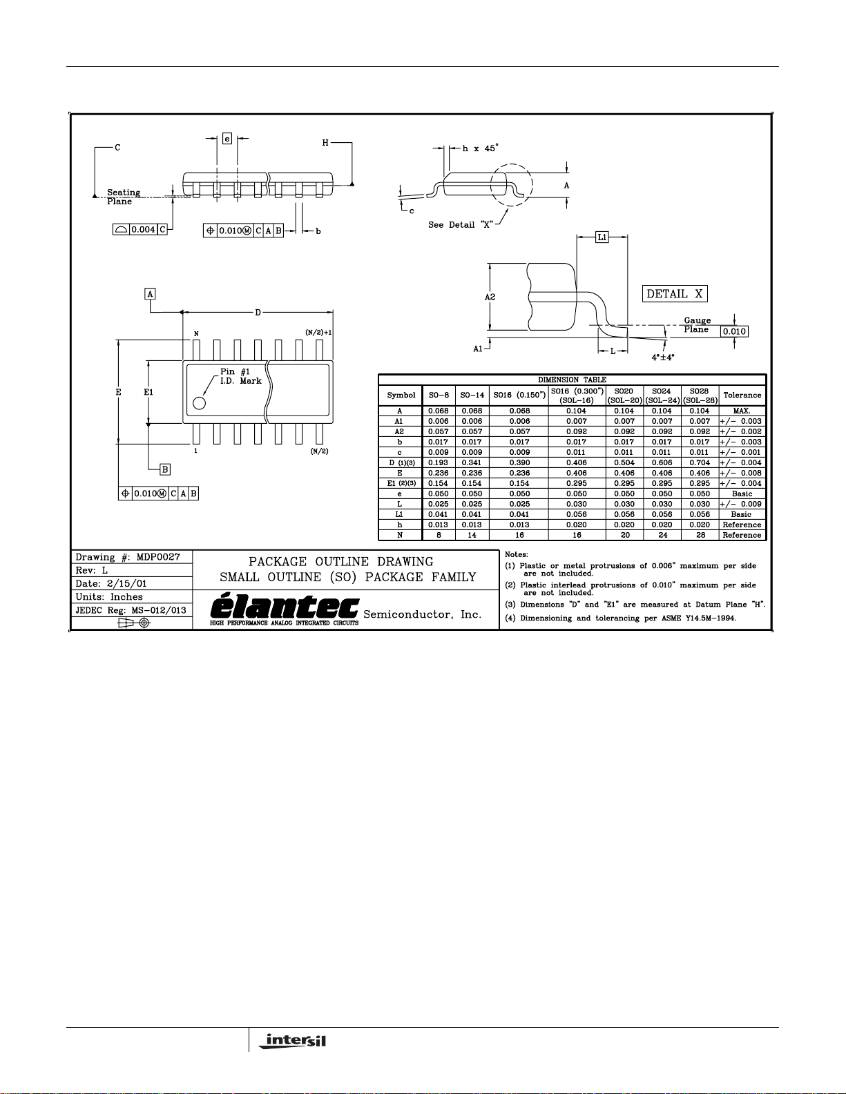
Package Outline Drawing - 20-Pin SO (0.300”) Package
NOTE: The package drawing shown here may not be the latest version. To check the latest revision, please refer to the Intersil website at
<http://www.intersil.com/design/packages/index.asp>
16
FN7297.3
May 9, 2005
EL7564
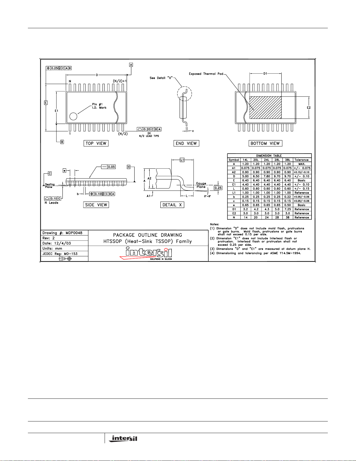
Package Outline Drawing (28-Pin HTSSOP Package)
NOTE: The package drawing shown here may not be the latest version. To check the latest revision, please refer to the Intersil website at
<http://www.intersil.com/design/packages/index.asp>
All Intersil U.S. products are manufactured, assembled and tested utilizing ISO9000 quality systems.
Intersil Corporation’s quality certifications can be viewed at www.intersil.com/design/quality
Intersil products are sold by description only. Intersil Corporation reserves the right to make changes in circuit design, software and/or specifications at any time without
notice. Accordingly, the reader is cautioned to verify that data sheets are current before placing orders. Information furnished by Intersil is believed to be accurate and
reliable. However, no responsibility is assumed by Intersil or its subsidiaries for its use; nor for any infringements of patents or other rights of third parties which may result
from its use. No license is granted by implication or otherwise under any patent or patent rights of Intersil or its subsidiaries.
For information regarding Intersil Corporation and its products, see www.intersil.com
17
FN7297.3
May 9, 2005

WWW.ALLDATASHEET.COM
Copyright © Each Manufacturing Company.
All Datasheets cannot be modified without permission.
This datasheet has been download from :
www.AllDataSheet.com
100% Free DataSheet Search Site.
Free Download.
No Register.
Fast Search System.
www.AllDataSheet.com
 Loading...