

S
N
G
I
®
D
E
D
N
E
M
M
O
C
E
R
T
O
N
O
P
E
L
B
I
S
S
T
S
B
U
S
9
L
S
I
R
O
F
T
U
T
I
6
3
5
7
E
N
P
E
Data Sheet
W
R
S
E
D
T
C
U
D
O
July 13, 2006
EL7536
FN7396.8
Monolithic 1A Step-Down Regulator
The EL7536 is a synchronous, integrated FET 1A step-down
regulator with internal compensation. It operates with an
input voltage range from 2.5V to 5.5V , which accommodates
supplies of 3.3V, 5V, or a Li-Ion battery source. The output
can be externally set from 0.8V to V
with a resistive
IN
divider.
The EL7536 features PWM mode control. The operating
frequency is typically 1.4MHz. Additional features include a
100ms Power-On-Reset output, <1µA shut-down current,
short-circuit protection, and over-temperature protection.
The EL7536 is available in the 10 Ld MSOP package,
making the entire converter occupy less than 0.15in
2
of PCB
area with components on one side only. Both packages are
specified for operation over the full -40°C to +85°C
temperature range.
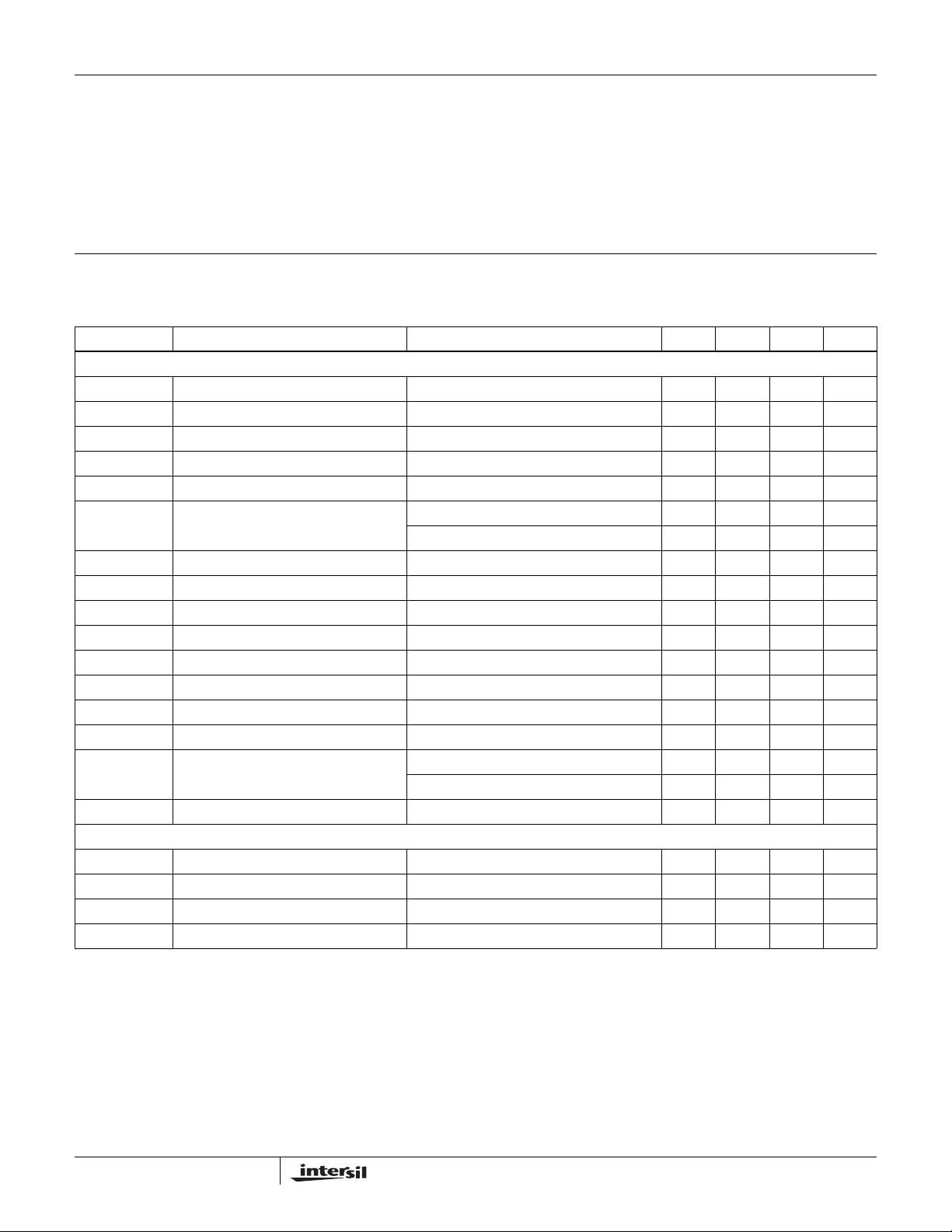
Ordering Information
PART NUMBER
(BRAND)
EL7536IY BDAAA - 10 Ld MSOP MDP0043
EL7536IY-T7 BDAAA 7” 10 Ld MSOP MDP0043
EL7536IY-T13 BDAAA 13” 10 Ld MSOP MDP0043
EL7536IYZ
(Note)
EL7536IYZ-T7
(Note)
EL7536IYZ-T13
(Note)
NOTE: Intersil Pb-free plus anneal products employ special Pb-free
material sets; molding compounds/die attach materials and 100%
matte tin plate termination finish, which are RoHS compliant and
compatible with both SnPb and Pb-free soldering operations. Intersil
Pb-free products are MSL classified at Pb-free peak reflow
temperatures that meet or exceed the Pb-free requirements of
IPC/JEDEC J STD-020.
PART
MARKING
BFAAA - 10 Ld MSOP
BFAAA 7” 10 Ld MSOP
BFAAA 13” 10 Ld MSOP
TAPE &
REEL PACKAGE
(Pb-free)
(Pb-free)
(Pb-free)
PKG.
DWG. #
MDP0043
MDP0043
MDP0043
Pinout
EL7536 (10 LD MSOP)
TOP VIEW
Features
• Less than 0.15in2 (0.97cm2) footprint for the complete 1A
converter
• Components on one side of PCB
• Max height 1.1mm MSOP10
• 100ms Power-On-Reset output (POR)
• Internally-compensated voltage mode controller
• Up to 94% efficiency
• <1µA shut-down current
• Overcurrent and over-temperature protection
• Pb-free plus anneal available (RoHS compliant)
Applications
• PDA and pocket PC computers
• Bar code readers
• Cellular phones
• Portable test equipment
• Li-Ion battery powered devices
• Small form factor (SFP) modules
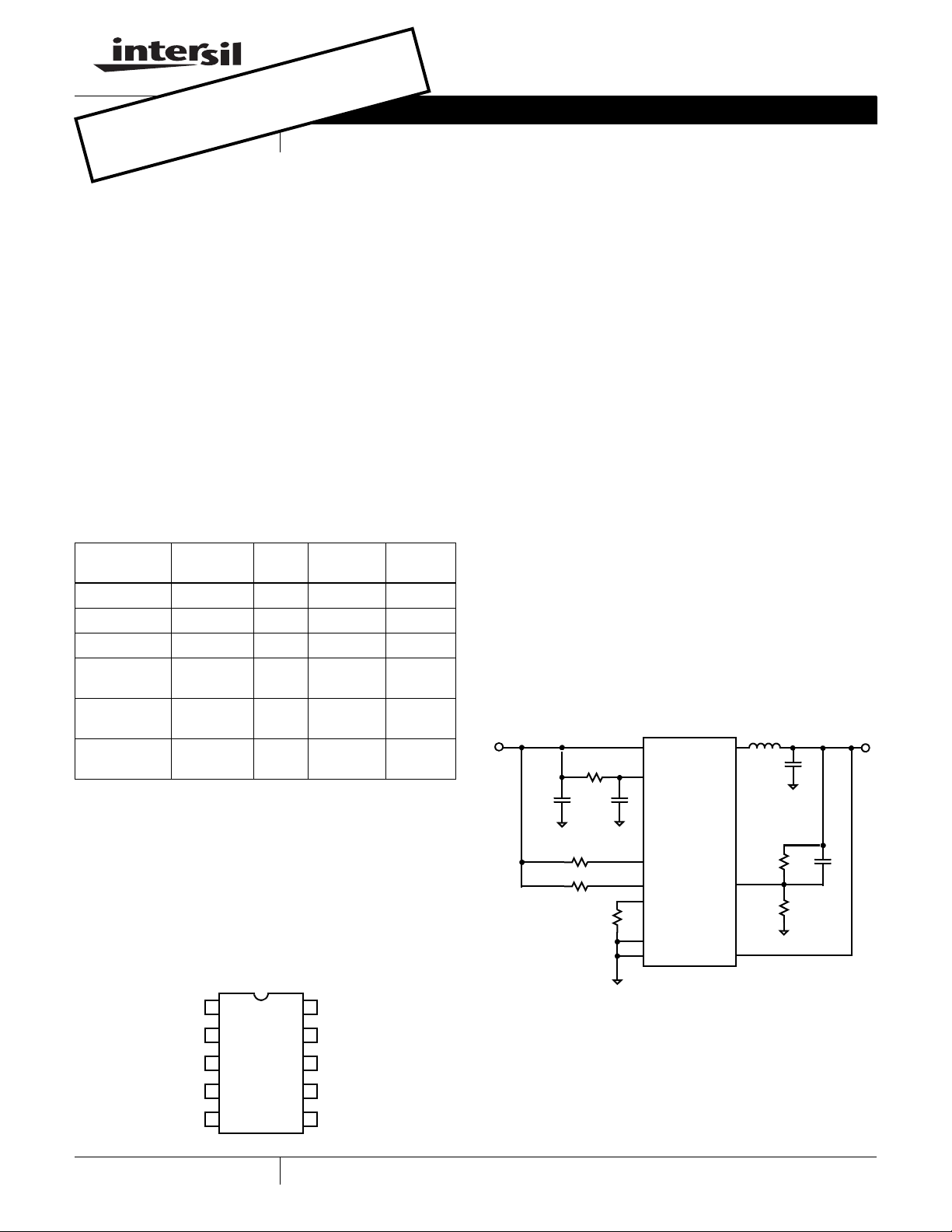
Typical Application Diagram
EL7536
TOP VIEW
V
S
C
10µF
(2.5V to 5.5V)
R3 100Ω
2
100kΩ
R
5
R4 100kΩ
100kΩ
C
0.1µF
R
L
VIN
VDD
3
EL7536
POR
EN
RSI
6
PGND
SGND
LX
FB
VO
1
1.8µH
10µF
R1*
124kΩ
R
100kΩ
C
1
*
2
(1.8V @ 1A)
C
470pF
4
V
O
SGND FB
1
PGND VO
2
LX POR
3
4
VIN EN
5 6
VDD RSI
1
10
9
8
7
CAUTION: These devices are sensitive to electrostatic discharge; follow proper IC Handling Procedures.
1-888-INTERSIL or 1-888-468-3774
All other trademarks mentioned are the property of their respective owners.
* V
= 0.8V * (1 + R1 / R2)
O
| Intersil (and design) is a registered trademark of Intersil Americas Inc.
Copyright © Intersil Americas Inc. 2003-2006. All Rights Reserved.
EL7536
Absolute Maximum Ratings (T
V
, VDD, POR to SGND. . . . . . . . . . . . . . . . . . . . . . -0.3V to +6.5V
IN
LX to PGND. . . . . . . . . . . . . . . . . . . . . . . . . . -0.3V to (V
RSI, EN, V
, FB to SGND. . . . . . . . . . . . . . . -0.3V to (VIN + +0.3V)
O
= 25°C)
A
+ +0.3V)
IN
Operating Ambient Temperature . . . . . . . . . . . . . . . .-40°C to +85°C
Storage Temperature. . . . . . . . . . . . . . . . . . . . . . . .-65°C to +150°C
Junction Temperature . . . . . . . . . . . . . . . . . . . . . . . . . . . . . .+125°C
PGND to SGND. . . . . . . . . . . . . . . . . . . . . . . . . . . . . -0.3V to +0.3V
Peak Output Current . . . . . . . . . . . . . . . . . . . . . . . . . . . . . . . . . 1.2A
CAUTION: Stresses above those listed in “Absolute Maximum Ratings” may cause permanent damage to the device. This is a stress only rating and operation of the
device at these or any other conditions above those indicated in the operational sections of this specification is not implied.
IMPORTANT NOTE: All parameters having Min/Max specifications are guaranteed. Typ values are for information purposes only . Unless otherwise noted, all tests are
at the specified temperature and are pulsed tests, therefore: T
Electrical Specifications V
DD
= V
IN
= TC = T
J
A
= VEN = 3.3V, C1 = C2 = 10µF, L = 1.8µH, VO = 1.8V, unless otherwise specified.
PARAMETER DESCRIPTION CONDITIONS MIN TYP MAX UNIT
DC CHARACTERISTICS
V
FB
I
FB
V
, V
IN
DD
V
IN,OFF
V
IN,ON
I
DD
R
DS(ON)-PMOS
R
DS(ON)-NMOS
I
LMAX
T
OT,OFF
T
OT,ON
I
, I
EN
RSI
V
, V
EN1
RSI1
V
, V
EN2
RSI2
V
POR
V
OLPOR
Feedback Input Voltage 790 800 810 mV
Feedback Input Current 250 nA
Input Voltage 2.5 5.5 V
Minimum Voltage for Shutdown VIN falling 2 2.2 V
Maximum Voltage for Startup VIN rising 2.2 2.4 V
Supply Current PWM, VIN = VDD = 5V 400 500 µA
EN = 0, V
= VDD = 5V 0.1 1 µA
IN
PMOS FET Resistance VDD = 5V, wafer test only 70 100 mΩ
NMOS FET Resistance VDD = 5V, wafer test only 45 75 mΩ
Current Limit 1.5 A
Over-temperature Threshold T rising 145 °C
Over-temperature Hysteresis T falling 130 °C
EN, RSI Current VEN, V
= 0V and 3.3V -1 1 V
RSI
EN, RSI Rising Threshold VDD = 3.3V 2.4 V
EN, RSI Falling Threshold VDD = 3.3V 0.8 V
Minimum VFB for POR, WRT Targeted
V
Value
FB
POR Voltage Drop I
rising 95 %
V
FB
falling 86 %
V
FB
= 5mA 35 70 mV
SINK
AC CHARACTERISTICS
F
t
RSI
t
SS
t
POR
PWM
PWM Switching Frequency 1.4 1.5 1.75 MHz
Minimum RSI Pulse Width Guaranteed by design 25 50 ns
Soft-start Time 650 µs
Power On Reset Delay Time 80 100 120 ms
2
FN7396.8
July 13, 2006
EL7536
Pin Descriptions
PIN NUMBER PIN NAME PIN FUNCTION
1 SGND Negative supply for the controller stage
2 PGND Negative supply for the power stage
3 LX Inductor drive pin; high current digital output with average voltage equal to the regulator output voltage
4 VIN Positive supply for the power stage
5 VDD Power supply for the controller stage
6 RSI Resets POR timer
7 EN Enable
8 POR Power on reset open drain output
9 VO Output voltage sense
10 FB Voltage feedback input; connected to an external resistor divider between V
output
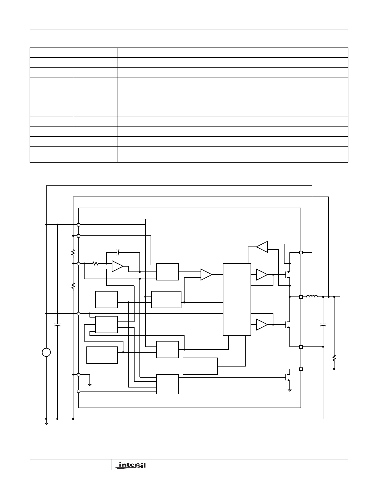
Block Diagram
and SGND for variable
O
EN
2.5V-
3.5V
10µF
+
–
124K
100K
V
DD
V
O
FB
EN
BANDGAP
REFERENCE
SGND
RSI
5M
CLOCK
1.4MHz
SOFT-
START
10pF
-
+
PWM
COMPEN-
SATION
RAMP
GENERATOR
UNDERVOLTAGE
LOCKOUT
POR
+
-
PWM
COMPARATOR
TEMPERATURE
SENSE
CONTROL
LOGIC
+
-
CURRENT
LIMIT
P-DRIVER
N-DRIVER
V
LX
PGND
POR
IN
1.8µ
1.8V
1A
10µF
100K
PG
3
FN7396.8
July 13, 2006
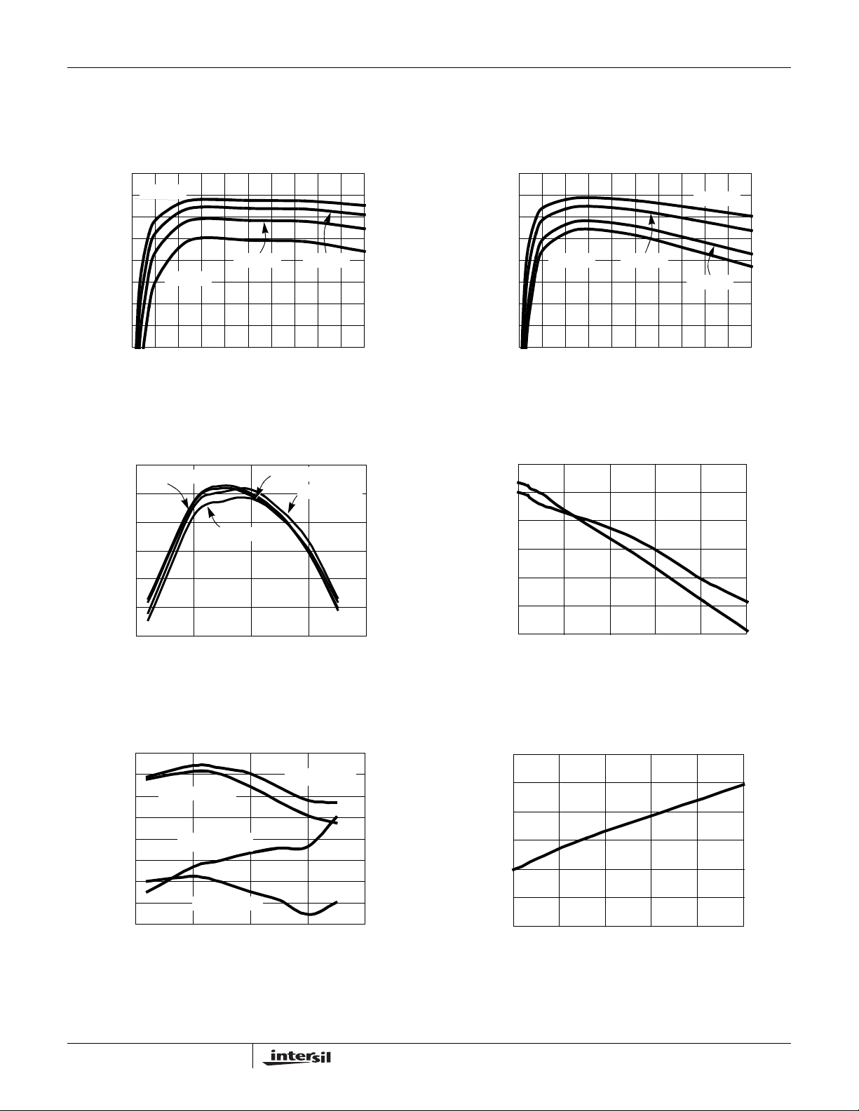
Performance Curves and Waveforms
All waveforms are taken at V
noted.
= 3.3V , VO = 1.8V , IO = 1A with component values shown on page 1 at room ambient temperature, unless otherwise
IN
EL7536
VIN=5V
100
VO=3.3V
95
90
85
80
75
EFFICIENCY (%)
70
65
60
VO=1.2V
0 200 400 600 800 1000
(mA)
I
O
FIGURE 1. EFFICIENCY FIGURE 2. EFFICIENCY
1.44
VIN=5V IO=1A
1.42
1.4
(MHz)
1.38
S
F
1.36
VIN=3.3V IO=0A
VIN=3.3V IO=1A
VIN=5V IO=0A
VIN=3.3V
100
95
90
85
VO=2.5VVO=1.8V
EFFICIENCY (%)
0.1%
0.0%
-0.1%
-0.2%
CHANGES
O
V
-0.3%
80
75
70
65
60
VO=1V
0 200 400 600 800 1000
VO=1.8V
(mA)
I
O
VIN=5V
VO=2.5V
VO=1.2V
VIN=3.3V
1.34
1.32
-50 0 50 100 150
T
(°C)
A
FIGURE 3. F
0.1%
0.0%
-0.1%
-0.2%
-0.3%
CHANGES
-0.4%
O
V
-0.5%
-0.6%
-0.7%
-50 0 50 100 150
vs JUNCTION TEMPERATURE
S
VIN=3.3V IO=0A
VIN=3.3V IO=1A
VIN=5V IO=1A
T
(°C)
J
VIN=5V IO=0A
FIGURE 5. LOAD/LINE REGULATIONS vs JUNCTION
TEMPERATURE
-0.4%
-0.5%
0 0.2 0.4 0.6 0.8 1
(A)
I
O
FIGURE 4. LOAD REGULATIONS
12
10
8
6
(mA)
IN
I
4
2
0
2.5 3
3.5
44.55
V
(V)
IN
FIGURE 6. NO LOAD INPUT CURRENT
4
FN7396.8
July 13, 2006

EL7536
Performance Curves and Waveforms (Continued)
All waveforms are taken at V
noted.
= 3.3V , VO = 1.8V , IO = 1A with component values shown on page 1 at room ambient temperature, unless otherwise
IN
0.5ms/d
FIGURE 7. START-UP 1
V
IN
(1V/d)
I
IN
(0.5A/d)
V
O
(1V/d)
V
IN
(2V/d)
V
O
(2V/d)
RSI
(2V/d)
POR
(2V/d)
V
IN
(2V/d)
V
O
(2V/d)
POR
(2V/d)
50ms/d
FIGURE 8. START-UP 2
0.75A
I
O
ΔV
O
0.25A
20mV/d
50ms/d
0.2ms/d
FIGURE 9. POR FUNCTION FIGURE 10. TRANSIENT RESPONSE
ΔV
ΔV
IN
i
L
V
LX
O
1µs/d
100mV/d
0.5A/d
2V/d
10mV/d
FIGURE 11. STEADY-STATE
5
FN7396.8
July 13, 2006

EL7536
Performance Curves and Waveforms (Continued)
All waveforms are taken at V
noted.
= 3.3V , VO = 1.8V , IO = 1A with component values shown on page 1 at room ambient temperature, unless otherwise
IN
JEDEC JESD51-3 LOW EFFECTIVE THERMAL
CONDUCTIVITY TEST BOARD
0.6
0.5
0.4
0.3
0.2
0.1
0
ALLOWABLE POWER DISSIPATION (W)
0 255075100 150
M
θ
S
J
O
A
P
=
1
2
0
0
6
°
C
/
W
85
AMBIENT TEMPERATURE (°C)
125
FIGURE 12. PACKAGE POWER DISSIPA TION vs AMBIENT
TEMPERATURE
JEDEC JESD51-7 HIGH EFFECTIVE THERMAL
CONDUCTIVITY TEST BOARD
1.00
0.90
0.80
0.70
0.60
0.50
0.40
0.30
0.20
0.10
0
ALLOWABLE POWER DISSIPATION (W)
0 255075100 150
M
θ
S
J
O
A
P
=
1
1
1
0
5
°
C
/
W
85
AMBIENT TEMPERATURE (°C)
125
FIGURE 13. PACKAGE POWER DISSIPA TION vs AMBIENT
TEMPERATURE
6
FN7396.8
July 13, 2006

V
EL7536
Applications Information
Product Description
The EL7536 is a synchronous, integrated FET 1A step-down
regulator which operates from an input of 2.5V to 6V. The
output voltage is user-adjustable with a pair of external
resistors.
The internally-compensated controller makes it possible to
use only two ceramic capacitors and one inductor to form a
complete, very small footprint 1A DC:DC converter.
Start-Up and Shut-Down
When the EN pin is tied to VIN, and VIN reaches
approximately 2.4V, the regulator begins to switch. The
output voltage is gradually increased to ensure proper softstart operation.
When the EN pin is connected to a logic low, the EL7536 is
in the shut-down mode. All the control circuitry and both
MOSFETs are off, and V
total input current is less than 1µA.
When the EN reaches logic HI, the regulator repeats the
start-up procedure, including the soft-start function.
PWM Operation
In the PWM mode, the P channel MOSFET and N channel
MOSFET always operate complementary. When the
PMOSFET is on and the NMOSFET off, the inductor current
increases linearly. The input energy is transferred to the
output and also stored in the inductor. When the P channel
MOSFET is off and the N channel MOSFET on, the inductor
current decreases linearly, and energy is transferred from
the inductor to the output. Hence, the average current
through the inductor is the output current. Since the inductor
and the output capacitor act as a low pass filter, the duty
cycle ratio is approximately equal to V
The output LC filter has a second order effect. To maintain
the stability of the converter, the overall controller must be
compensated. This is done with the fixed internally
compensated error amplifier and the PWM compensator.
Because the compensations are fixed, the value s of input
and output capacitors are 10µF to 22µF ceramic. The
inductor is nominally 1.8µH, but 1.5µA to 2.2µH can be used.
100% Duty Ratio Operation
EL7536 utilizes CMOS power FET's as the internal
synchronous power switches. The upper switch is a PMOS
and lower switch a NMOS. This not only saves a boot
capacitor, it also allows 100% turn-on of the upper PFET
switch, achieving V
V
is,
O
OVINRLRDSON1
close to VIN. The maximum achievable
O
+()IO×–=
falls to zero. In this mode, the
OUT
divided by VIN.
O
Where RL is the DC resistance on the inductor and R
DSON1
the PFET on-resistance, nominal 70mΩ at room temperature
with tempco of 0.2mΩ/°C.
As the input voltage drops gradually close or even below the
preset V
, the converter gets into 100% duty ratio. At this
O
condition, the upper PFET needs some minimum turn-off
time if it is turned off. This off-time is related to input/output
conditions. This makes the duty ratio appears randomly and
increases the output ripple somewhat until the 100% duty
ratio is reached. Larger output capacitor could reduce the
random-looking ripple. Users need to verify if this condition
has adverse effect on overall circuit if close to 100% duty
ratio is expected.
RSI/POR Function
When powering up, the open-collector Power-On-Reset
output holds low for about 100ms after V
reaches the
O
preset voltage. When the active-HI reset signal RSI is
issued, POR goes to low immediately and holds for the
same period of time after RSI comes back to LOW. The
output voltage is unaffected. (Please refer to the timing
diagram). When the function is not used, connect RSI to
ground and leave open the pull-up resister R
at POR pin.
4
The POR output also serves as a 100ms delayed Power
Good signal when the pull-up resister R
is installed. The
4
RSI pin needs to be directly (or indirectly through a resister
R
) connected to Ground for this to function properly.
6
V
O
RSI
100ms
POR
FIGURE 14. RSI & POR TIMING DIAGRAM
MIN
25ns
100ms
Output Voltage Selection
Users can set the output voltage of the converter with a
resister divider, which can be chosen based on the following
formula:
R
⎛⎞
2
0.8 1
V
O
-------
+
×=
⎜⎟
R
⎝⎠
1
Component Selection
Because of the fixed internal compensation, the component
choice is relatively narrow. We recommend 10µF to 22µF
multi-layer ceramic capacitors with X5R or X7R rating for
both the input and output capacitors, and 1.5µH to 2.2µH
inductance for the inductor.
7
FN7396.8
July 13, 2006

At extreme conditions (VIN < 3V, IO > 0.7A, and junction
temperature higher than 75°C), input cap C
is
1
recommended to be 22µF. Otherwise, if any of the above 3
conditions is not true, C
can remain as low as 10µF.
1
The RMS current present at the input capacitor is decided by
the following formula:
This is about half of the output current IO for all the VO. This
input capacitor must be able to handle this current.
The inductor peak-to-peak ripple current is given as:
• L is the inductance
•f
the switching frequency (nominally 1.4MHz)
S
The inductor must be able to handle I
for the RMS load
O
current, and to assure that the inductor is reliable, it must
handle the 1.5A surge current that can occur during a
current limit condition.
In addition to decoupling capacitors and inductor value, it is
important to properly size the phase-lead capacitor C
4
(Refer to the Typical Application Diagram). The phase-lead
capacitor creates additional phase margin in the control loop
by generating a zero and a pole in the transfer function. As a
general rule of thumb, C
should be sized to start the phase-
4
lead at a frequency of ~2.5kHz. The zero will always appear
at lower frequency than the pole and follow the equation
below:
Over a normal range of R
(~10-100k), C4 will range from
2
~470-4700pF. The pole frequency cannot be set once the
zero frequency is chosen as it is dictated by the ratio of R
and R
, which is solely determined by the desired output set
2
point. The equation below shows the pole frequency
relationship:
Current Limit and Short-Circuit Protection
8
1
FN7396.8
July 13, 2006

Mini SO Package Family (MSOP)
M
C
SEATING
PLANE
0.10 C
N LEADS
0.25 C A B
E1E
B
L1
D
N
1
e
b
A
(N/2)+1
PIN #1
I.D.
(N/2)
H
M
0.08 C A B
A
EL7536
MDP0043
MINI SO PACKAGE FAMILY
SYMBOL MSOP8 MSOP10 TOLERANCE NOTES
A1.101.10 Max. A1 0.10 0.10 ±0.05 A2 0.86 0.86 ±0.09 -
b 0.33 0.23 +0.07/-0.08 -
c0.180.18 ±0.05 D 3.00 3.00 ±0.10 1, 3
E4.904.90 ±0.15 -
E1 3.00 3.00 ±0.10 2, 3
e0.650.50 Basic -
L0.550.55 ±0.15 -
L1 0.95 0.95 Basic -
N 8 10 Reference -
Rev. C 6/99
NOTES:
1. Plastic or metal protrusions of 0.15mm maximum per side are not
included.
2. Plastic interlead protrusions of 0.25mm maximum per side are
not included.
3. Dimensions “D” and “E1” are measured at Datum Plane “H”.
4. Dimensioning and tolerancing per ASME Y14.5M-1994.
c
SEE DETAIL "X"
A2
GAUGE
A1
L
DETAIL X
PLANE
3° ±3°
0.25
All Intersil U.S. products are manufactured, assembled and tested utilizing ISO9000 quality systems.
Intersil Corporation’s quality certifications can be viewed at www.intersil.com/design/quality
Intersil products are sold by description only. Intersil Corporation reserves the right to make changes in circuit design, software and/or specifications at any time without
notice. Accordingly, the reader is cautioned to verify that data sheets are current before placing orders. Information furnished by Intersil is believed to be accurate and
reliable. However, no responsibility is assumed by Intersil or its subsidiaries for its use; nor for any infringements of patents or other rights of third parties which may result
from its use. No license is granted by implicat ion or oth erwise u nde r any p a tent or p at ent r ights of Intersil or its subsidiaries.
For information regarding Intersil Corporation and its products, see www.intersil.com
9
FN7396.8
July 13, 2006
 Loading...