intersil EL7515 DATA SHEET

®
www.BDTIC.com/Intersil
EL7515
Data Sheet August 10, 2007
High Frequency PWM Step-Up Regulator
The EL7515 is a high frequency, high efficiency step-up
DC/DC regulator operated at fixed frequency PWM mode.
With an integrated 1.4A MOSFET , it can deliver up to 600mA
output current at up to 92% efficiency. The adjustable
switching frequency is up to 1.2MHz, making it ideal for DSL
applications.
When shut down, it draws <1µA of current. This feature,
along with the minimum starting voltage of 1.8V, makes it
suitable for portable equipment powered by one Lithium Ion,
3 to 4 NiMH cells, or 2 cells of alkaline battery.
The EL7515 is available in a 10 Ld MSOP package, with
maximum height of 1.1mm. With proper external
components, the whole converter takes less than 0.25in
2
PCB space.
This device is specified for operation over the full -40°C to
+85°C temperature range.
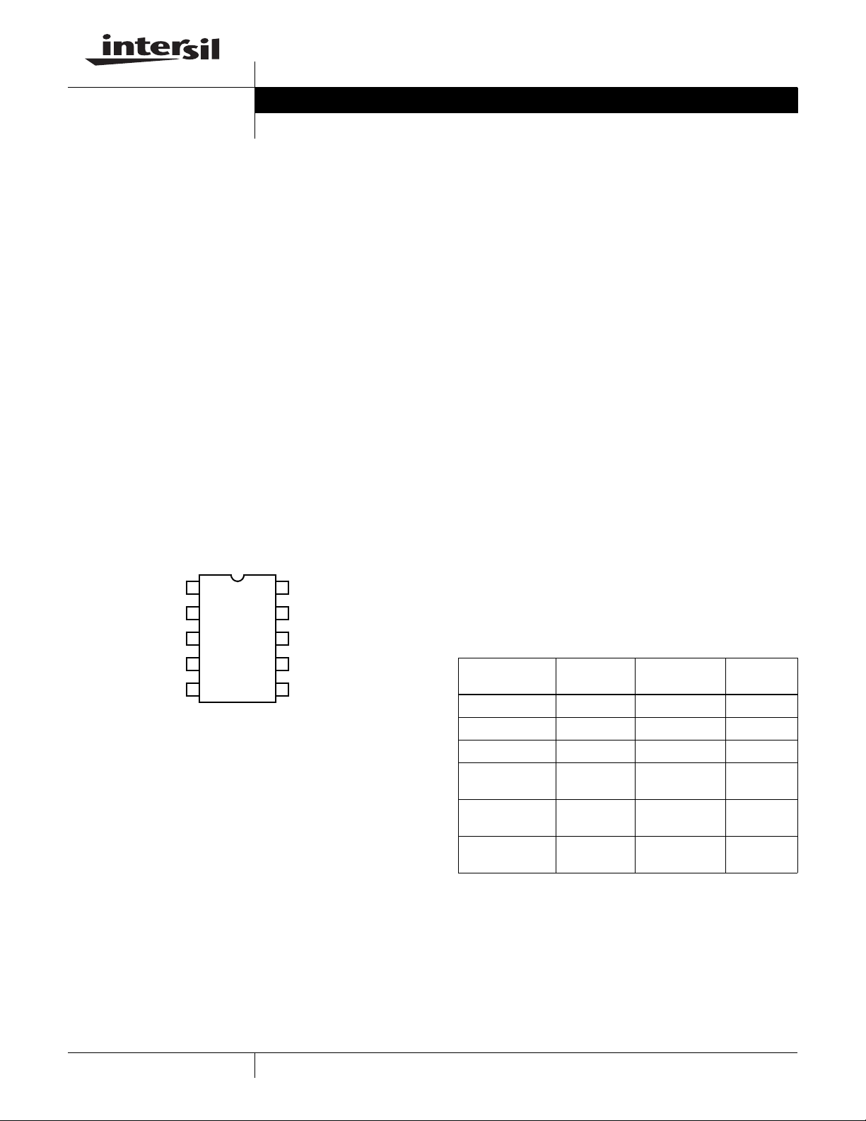
Pinout
EL7515
(10 LD MSOP)
TOP VIEW
PGND
SGND
1
2
LX
10
VDD
9
Features
• Up to 92% efficiency
• Up to 600mA I
•4.5V < V
•1.8V < V
< 17V
OUT
< 13.2V
IN
OUT
• Up to 1.2MHz adjustable frequency
• <1µA shutdown current
• Adjustable soft-start
• Low battery detection
• Internal thermal protection
• 1.1mm max height 10 Ld MSOP package
• Pb-Free available (RoHS compliant)
Applications
• 3V to 5V and 12V converters
• 5V to 12V converters
•TFT-LCD
•DSL
• Portable equipment
• Desktop equipment
FN7120.2
RT
3
EN
4
5 6
FB
8
SS
7
LBOLBI
Ordering Information
PART
NUMBER
EL7515IY e 10 Ld MSOP MDP0043
EL7515IY-T7* e 10 Ld MSOP MDP0043
EL7515IY-T13* e 10 Ld MSOP MDP0043
EL7515IYZ
(Note)
EL7515IYZ-T7*
(Note)
EL7515IYZ-T13*
(Note)
*Please refer to TB347 for details on reel specifications.
NOTE: These Intersil Pb-free plastic packaged products employ
special Pb-free material sets; molding compounds/die attach
materials and 100% matte tin plate PLUS ANNEAL - e3 termination
finish, which is RoHS compliant and compatible with both SnPb and
Pb-free soldering operations. Intersil Pb-free products are MSL
classified at Pb-free peak reflow temperatures that meet or exceed
the Pb-free requirements of IPC/JEDEC J STD-020.
PART
MARKING PACKAGE
BAAAR 10 Ld MSOP
(Pb-free)
BAAAR 10 Ld MSOP
(Pb-free)
BAAAR 10 Ld MSOP
(Pb-free)
PKG.
DWG. #
MDP0043
MDP0043
MDP0043
1
CAUTION: These devices are sensitive to electrostatic discharge; follow proper IC Handling Procedures.
1-888-INTERSIL or 1-888-468-3774
| Intersil (and design) is a registered trademark of Intersil Americas Inc.
Copyright Intersil Americas Inc. 2003, 2005, 2007. All Rights Reserved
All other trademarks mentioned are the property of their respective owners.

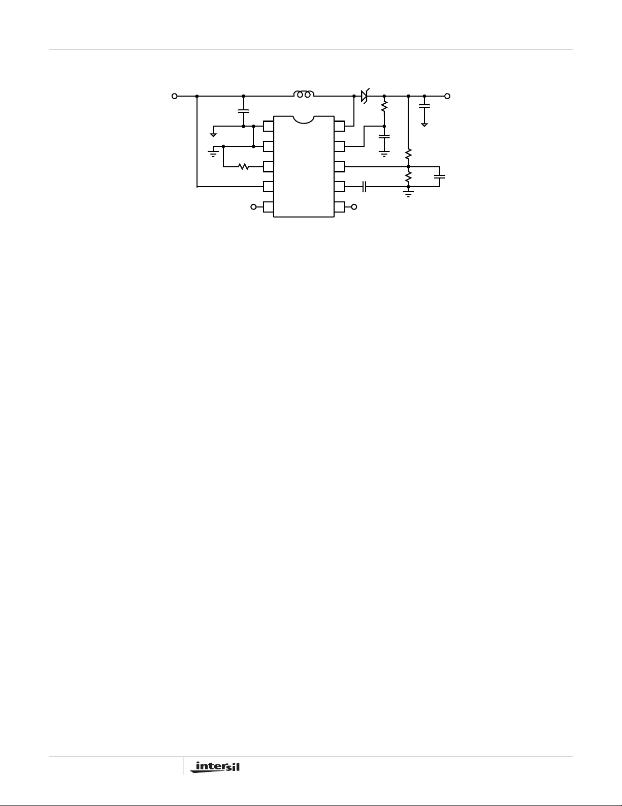
Typical Application
www.BDTIC.com/Intersil
(1.8V TO 9V)
EL7515
L
PGND
SGND
RT
EN
LBI
1
10µH
LX
VDD
FB
SS
LBO
V
IN
C
10µF
1
R
100kΩ
1
2
3
3
4
5 6
D
1
R
4
1.4kΩ
10
9
8
7
20nF
C
4
0.1µF
R
2
82kΩ
R
C
3
1
10kΩ
C
5
22µF
V
OUT
(12V UP TO
630mA)
C
10
4.7nF
2
FN7120.2
August 10, 2007

EL7515
www.BDTIC.com/Intersil
Absolute Maximum Ratings (T
EN, LBI, VDD. . . . . . . . . . . . . . . . . . . . . . . . . . . . . . . . . . . . . . .+12V
LX . . . . . . . . . . . . . . . . . . . . . . . . . . . . . . . . . . . . . . . . . . . . . . .+18V
CAUTION: Do not operate at or near the maximum ratings listed for extended periods of time. Exposure to such conditions may adversely impact product reliability and
result in failures not covered by warranty.
IMPORTANT NOTE: All parameters having Min/Max specifications are guaranteed. Typ values are for informati on purposes only. Unless otherwise noted, all tests are
at the specified temperature and are pulsed tests, therefore: T
Electrical Specifications V
PARAMETER DESCRIPTION CONDITIONS
V
IN
V
OUT
IQ1 Quiescent Current - Shut-down V
IQ2 Quiescent Current V
V
FB
IB Feedback Input Bias Current 0.10 µA
D
MAX
I
LIM
I
SHDN
V
LBI
V
OL-LBO
I
LEAK-LBO
r
DS(ON)
I
LEAK-SWITCH
/ΔVIN/V
ΔV
OUT
ΔV
OUT/VOUT
f
OSC-MAX
f
OSC1
VHI_EN EN Input High Threshold 1.6 V
VLO_EN EN Input Low Threshold 0.5 V
Input Voltage Range 1.8 13.2 V
Output Voltage Range 4.5 17 V
Feedback Voltage 1.29 1.33 1.37 V
Maximum Duty Cycle 84 90 %
Current Limit - Max Peak Input
Current
Shut-down Input Bias Current 1µA
LBI Threshold Voltage 180 220 250 mV
LBO Output Low I
LBO Output Leakage Current V
Switch On Resistance at 12V output 220 mΩ
Switch Leakage Current 1µA
Line Regulation 3V < V
OUT
Load Regulation I
Maximum Switching Frequency RT = 49.9kΩ 1200 kHz
Switching Frequency 600 670 750 kHz
= +25°C) Thermal Information
A
Storage Temperature. . . . . . . . . . . . . . . . . . . . . . . .-65°C to +150°C
Operating Temperature . . . . . . . . . . . . . . . . . . . . . . .-40°C to +85°C
Operating Junction Temperature: . . . . . . . . . . . . . . . . . . . . .+135°C
Pb-free reflow profile . . . . . . . . . . . . . . . . . . . . . . . . . .see link below
http://www.intersil.com/pbfree/Pb-FreeReflow.asp
= TC = T
IN
= 5V, V
J
= 12V, L = 10µH, I
OUT
A
= 0mA, RT = 100kΩ, TA = +25°C, Unless Otherwise Specified.
OUT
= 0, feedback resistors disconnected 1 µA
EN
= 2V 1.4 2 mA
EN
= 1mA 0.1 0.2 V
LBO
= 250mV, V
LBI
< 6V, V
IN
= 50mA to 150mA 1 %
OUT
= 5V 0.02 2 µA
LBO
= 12V, no load 0.4 %/V
OUT
MIN
(Note 1) TYP
11.4 A
MAX
(Note 1) UNIT
Pin Descriptions
PIN NUMBER PIN NAME PIN FUNCTION
1 PGND Power ground; connected to the source of internal N-Channel power MOSFET
2 SGND Signal ground; ground reference for all the control circuitry; needs to have only a single connection to PGND
3 RT Timing resistor to adjust the oscillation frequency of the converter
4 EN Chip enable; connects to logic HI (>1.6V) for chip to function
5 LBI Low battery input; connects to a sensing voltage, or left open if function is not used
6 LBO Low battery detection output; connected to the open drain of a MOSFET; able to sink 1mA current
7 SS Soft-start; connects to a capacitor to control the start-up of the converter
8 FB Voltage feedback input; needs to connect to resistor divider to decide V
9 VDD Control circuit positive supply
10 LX Inductor drive pin; connected to the drain of internal N-Channel power MOSFET
3
O
FN7120.2
August 10, 2007
 Loading...