Intersil Corporation EL7513IY-T7, EL7513IY-T13, EL7513IY, EL7513IWT-T7, EL7513IWT Datasheet

1
®
FN7112.2
EL7513
White LED Step-Up Regulator
The EL7513 is a constant current
boost regulator specially designed for
driving white LEDs. It can drive 4
LEDs in series or up to 12 LEDs in parallel/series
configuration and achieves efficiency up to 91%.
The brightness of the LEDs is adjusted through a voltage
level on the CNTL pin. When the level falls below 0.1V, the
chip goes into shut-down mode and consumes less than
1µA of supply current for V
IN
less than 5.5V.
The EL7513 is available in the 8-pin TSOT and 8-pin MSOP
packages. The TSOT package is just 1mm high, compared
to 1.45mm for the standard SOT23 package.
Features
• 2.6V to 13.2V input voltage
• 18V maximum output voltage
• Drives up to 12 LEDs
• 1MHz switching frequency
• Up to 91% efficiency
• 1µA maximum shut-down current
• Dimming control
• 8-pin TSOT and 8-pin MSOP packages
Applications
•PDAs
• Cellular phones
• Digital cameras
• White LED backlighting
Ordering Information
PAR T
NUMBER PACKAGE
TAPE &
REEL PKG. DWG. #
EL7513IWT 8-Pin TSOT - MDP0049
EL7513IWT-T7 8-Pin TSOT 7” MDP0049
EL7513IWT-T13 8-Pin TSOT 13” MDP0049
EL7513IY 8-Pin MSOP - MDP0043
EL7513IY-T7 8-Pin MSOP 7” MDP0043
EL7513IY-T13 8-Pin MSOP 13” MDP0043
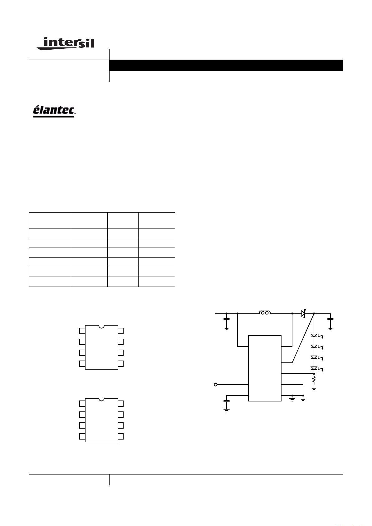
Pinouts Typical Connection
EL7513
(8-PIN TSOT)
TOP VIEW
EL7513
(8-PIN MSOP)
TOP VIEW
COMP
CNTL
VOUT
LX
VIN
CS
SGND
PGND
1
2
3
4
8
7
6
5
CS
VIN
PGND
SGND
CNTL
COMP
LX
VOUT
1
2
3
4
8
7
6
5
C
1
LXVIN
VOUT
CS
PGND
SGND
CNTL
COMP
4.7µF
C
3
0.1µF
C
2
1µF
L
33µH
D
2.6V TO
5.5V
R
1
V
CTRL
5Ω
Data Sheet July 2003
CAUTION: These devices are sensitive to electrostatic discharge; follow proper IC Handling Procedures.
1-888-INTERSIL or 321-724-7143
| Intersil (and design) is a registered trademark of Intersil Americas Inc.
Copyright © Intersil Americas Inc. 2003. All Rights Reserved. Elantec is a registered trademark of Elantec Semiconductor, Inc.
All other trademarks mentioned are the property of their respective owners.

2
IMPORTANT NOTE: All parameters having Min/Max specifications are guaranteed. Typ values are for information purposes only. Unless otherwise noted, all tests are
at the specified temperature and are pulsed tests, therefore: T
J
= TC = T
A
Absolute Maximum Ratings (T
A
= 25°C)
COMP, CNTL, CS to SGND. . . . . . . . . . . . . . . . . . . . . . -0.3V to +6V
V
IN
to SGND . . . . . . . . . . . . . . . . . . . . . . . . . . . . . . . . . . . . . . .+14V
V
OUT
to SGND . . . . . . . . . . . . . . . . . . . . . . . . . . . . . . . . . . . . .+19V
LX to PGND . . . . . . . . . . . . . . . . . . . . . . . . . . . . . . . . . . . . . . . .+20V
SGND to PGND . . . . . . . . . . . . . . . . . . . . . . . . . . . . . -0.3V to +0.3V
Storage Temperature . . . . . . . . . . . . . . . . . . . . . . . . -65°C to +150°C
Ambient Operating Temperature . . . . . . . . . . . . . . . . -40°C to +85°C
CAUTION: Stresses above those listed in “Absolute Maximum Ratings” may cause permanent damage to the device. This is a stress only rating and operation of the
device at these or any other conditions above those indicated in the operational sections of this specification is not implied. This part is ESD sensitive. Handle with care.
Electrical Specifications V
IN
= 3V, VO = 12V, C1 = 4.7µF, L = 33µH, C2 = 1µF, C3 = 0.1µF, R1 = 5Ω, TA = 25°C,
Unless Otherwise Specified
PARAMETER DESCRIPTION CONDITIONS MIN TYP MAX UNIT
V
IN
Input Voltage 2.6 13.2 V
I
Q1
Total Input Current at Shut-down V
CNTL
= 0V 1 µA
I
Q1
Quiescent Supply Current at VO Pin V
CNTL
= 1V, load disconnected 1 1.5 mA
I
COMP
COMP Pin Pull-up Current COMP connected to SGND 11 20 µA
V
COMP
COMP Voltage Swing 0.5 1.5 2.5 V
I
CNTL
CNTL Shut-down Current CNTL = 0V 1 µA
V
CNTL1
Chip Enable Voltage 240 mV
V
CNTL2
Chip Disable Voltage 100 mV
I
OUT_ACCURACYVCNTL
= 1V V
CNTL
= 1V 14 15 16 mA
V
OUT1
Over-voltage Threshold V
OUT
rising 17 18 19 V
V
OUT2
Over-voltage Threshold V
OUT
falling, with resistive load 15 16 17.5 V
ILX MOSFET Current Limit 500 mA
R
DS_ON
MOSFET On-resistance 0.7 Ω
I
LEAK
MOSFET Leakage Current V
CNTL
= 0V, VLX = 12V 1 µA
F
S
Switching Frequency 800 1000 1200 kHz
D
MAX
Maximum Duty Ratio V
CNTL
= 2V, IS = 0 85 90 %
I
CS
CS Input Bias Current 1µA
∆I
O
/∆V
IN
Line Regulation VIN = 2.6V - 5.5V 0.03 %/V
Pin Descriptions
8-PIN TSOT 8-PIN MSOP PIN NAME DESCRIPTION
1 7 COMP Compensation pin. A compensation cap (4700pF to 1µF) is normally connected between this pin and
SGND.
2 8 CNTL Control pin for dimming and shut-down. A voltage between 250mV and 5.5V controls the brightness,
and less than 100mV shuts down the converter.
3 5 VOUT Output voltage sense. Use for over voltage protection.
4 6 LX Inductor connection pin. The drain of internal MOSFET.
5 3 PGND Power Ground pin. The source of internal MOSFET.
6 4 SGND Signal Ground. Ground pin for internal control circuitry. Needs to connect to PGND at only one point.
7 1 CS Current sense pin. Connect to sensing resistor to set the LED bias current.
8 2 VIN Power supply for internal control circuitry.
EL7513

3
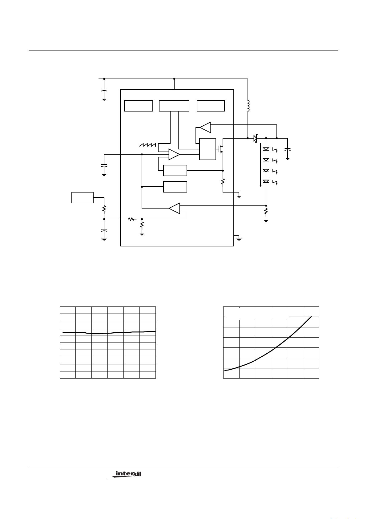
Block Diagram
REFERENCE
GENERATOR
1MHz
OSCILLATOR
THERMAL
SHUTDOWN
BOOST
I-SENSE
START-UP
CONTROL
+
+
-
+
+
PWM
SIGNAL
C
OUT
1µF
I(LED)
OVER-VOLTAGE
PROTECTION
ERROR AMP
CNTL
COMP
V
IN
C
IN
4.7µF
C
COMP
0.1µF
SGND
C
S
PGND
LX
V
OUT
L
33µH
2.6V TO
5.5V
5Ω
V
CNTL
PWM
LOGIC
617K
50K
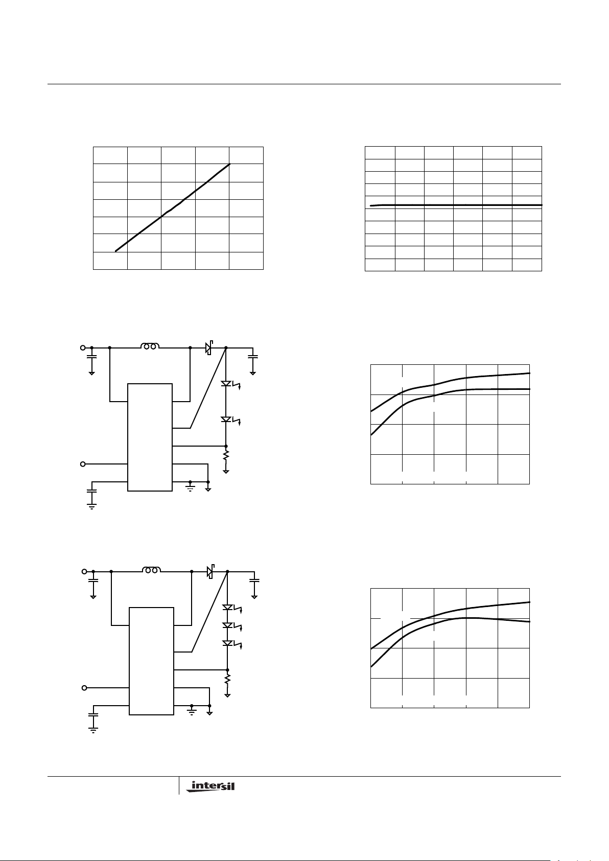
Typical Performance Curves
All performance curves and waveforms are taken with C1 = 4.7µF, C2 = 1µF, C3 = 0.1µF, L = 33µF, V
IN
= 3.3V, V
CNTL
= 1V, R1=5Ω, 4 LEDs in a
series; unless otherwise specified.
FIGURE 1. SWITCHING FREQUENCY vs V
IN
FIGURE 2. QUIESCENT CURRENT
1.05
1.04
1.02
1.01
1
2.5 3.5 4.5
V
IN
(V)
F
S
(MHz)
1.03
5.5345
3.5
2
1
0
2.5 6.5 10.5
V
IN
(V)
I
IN
(µA)
3
14.54.5 8.5 12.5
2.5
1.5
0.5
V
CNTL
=0V, 0.1V
WHITE LEDs DISCONNECTED
EL7513

4
FIGURE 3. I
LED
vs V
CNTL
FIGURE 4. I
LED
vs V
IN
FIGURE 5A. 2 LEDs IN A SERIES FIGURE 5B. EFFICIENCY vs I
O
FIGURE 5.
FIGURE 6A. 3 LEDs IN A SERIES FIGURE 6B. EFFICIENCY vs I
O
FIGURE 6.
Typical Performance Curves (Continued)
All performance curves and waveforms are taken with C
1
= 4.7µF, C2 = 1µF, C3 = 0.1µF, L = 33µF, V
IN
= 3.3V, V
CNTL
= 1V, R1=5Ω, 4 LEDs in a
series; unless otherwise specified.
0
5
10
15
20
25
30
35
0 0.5 1 1.5 2 2.5
V
CNTL
(V)
I
LED
(mA)
14
14.2
14.4
14.6
14.8
15
15.2
15.4
15.6
15.8
16
2.53.54.55.5
V
IN
(V)
V
CNTL
=1V
I
LED
(mA)
34
5
LXVIN
VOUT
CS
PGND
SGND
CNTL
COMP
4.7µF
0.1µF
1µF
L
33µH
BAT54HT1
V
IN
25
16
3
7
48
V
CTRL
5Ω
2 LEDs IN A SERIES
90
85
80
75
70
5 1015202530
I
O
(mA)
EFFICIENCY (%)
L=COILCRAFT LPO1704-333CM
VIN=4.2V
VIN=2.7V
LXVIN
VOUT
CS
PGND
SGND
CNTL
COMP
4.7µF
0.1µF
1µF
L
33µH
BAT54HT1
V
IN
25
16
3
7
48
V
CTRL
5Ω
3 LEDs IN A SERIES
90
85
80
75
70
5 1015202530
I
O
(mA)
EFFICIENCY (%)
L=COILCRAFT LPO1704-333CM
VIN=4.2V
VIN=2.7V
EL7513
 Loading...