

®
www.BDTIC.com/Intersil
EL7457
Data Sheet January 3, 2005
40MHz Non-Inverting Quad CMOS Driver
The EL7457 is a high speed, non-inverting, quad CMOS
driver. It is capable of running at clock rates up to 40MHz
and features 2A peak drive capability and a nominal onresistance of just 3Ω. The EL7457 is ideal for driving highly
capacitive loads, such as storage and vertical clocks in CCD
applications. It is also well suited to ATE pin driving, levelshifting, and clock-driving applications.
The EL7457 is capable of running from single or dual power
supplies while using ground referenced inputs. Each output
can be switched to either the high (V
) or low (VL) supply
H
pins, depending on the related input pin. The inputs are
compatible with both 3V and 5V CMOS and TTL logic. The
output enable (OE) pin can be used to put the outputs into a
high-impedance state. This is especially useful in CCD
applications, where the driver should be disabled during
power down.
The EL7457 also features very fast rise and fall times which
are matched to within 1ns. The propagation delay is also
matched between rising and falling edges to within 2ns.
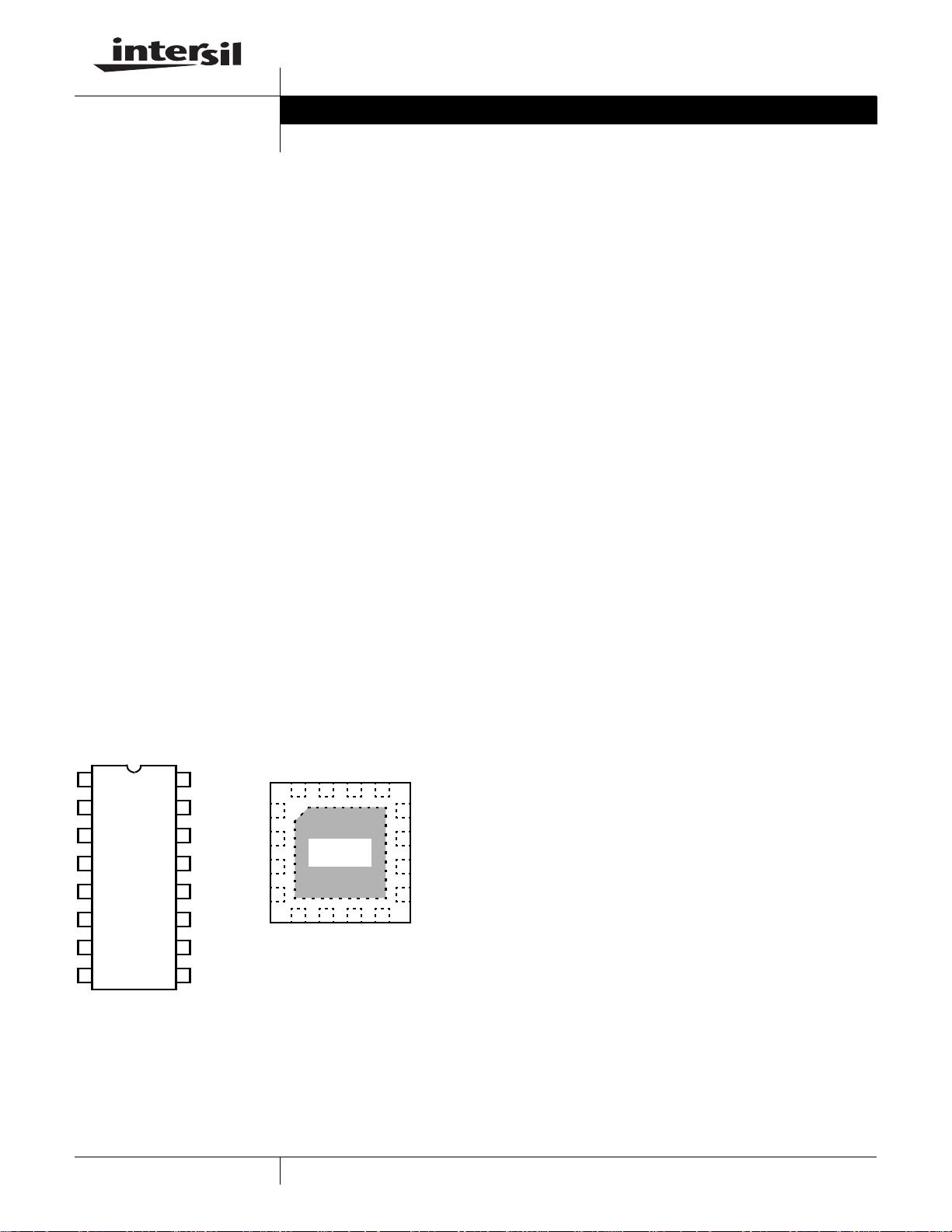
The EL7457 is available in 16-pin QSOP, 16-pin SO
(0.150"), and 16-pin QFN packages. All are specified for
operation over the full -40°C to +85°C temperature range.
Pinouts
EL7457
[16-PIN SO (0.150”),
QSOP (0.150”)]
TOP VIEW
INA
1
OE
2
INB
3
VL
4
GND
5
NC
6
INC
7
IND
8 9
VS+
OUTA
OUTB
NC
VH
OUTC
OUTD
VS-
16
15
14
13
12
11
10
INB
VL
VL
GND
* THERMAL PAD CONNECTED
TO PIN 7 (V
EL7457
[16-PIN QFN (4x4mm)]
TOP VIEW
OE
INA
VS+
OUTA
16
15
14
13
1
2
THERMAL
5
INC
S
PAD*
6
7
8
VS-
IND
-)
OUTD
3
4
12
11
10
9
OUTB
VH
VH
OUTC
Features
• Clocking speeds up to 40MHz
• 4 channels
• 12ns tR/tF at 1000pF C
LOAD
• 1ns rise and fall time match
• 1.5ns prop delay match
• Low quiescent current - <1mA
• Fast output enable function - 12ns
• Wide output voltage range
•8V ≥ V
•-2V ≤ V
≥ -5V
L
≤ 16.5V
H
• 2A peak drive
•3Ω on resistance
• Input level shifters
• TTL/CMOS input-compatible
• Pb-free available (RoHS compliant)
Applications
• CCD drivers
• Digital cameras
• Pin drivers
• Clock/line drivers
• Ultrasound transducer drivers
• Ultrasonic and RF generators
• Level shifting
FN7288.3
1
CAUTION: These devices are sensitive to electrostatic discharge; follow proper IC Handling Procedures.
1-888-INTERSIL or 321-724-7143
| Intersil (and design) is a registered trademark of Intersil Americas Inc.
All other trademarks mentioned are the property of their respective owners.
Copyright © Intersil Americas Inc. 2002-2005. All Rights Reserved.
Ordering Information
www.BDTIC.com/Intersil
EL7457
TAPE &
PART NUMBER PACKAGE
EL7457CU 16-Pin QSOP
EL7457CU-T7 16-Pin QSOP
EL7457CU-T13 16-Pin QSOP
EL7457CUZ
(See Note)
EL7457CUZ-T7
(See Note)
EL7457CUZ-T13
(See Note)
EL7457CS 16-Pin SO
EL7457CS-T7 16-Pin SO
EL7457CS-T13 16-Pin SO
NOTE: Intersil Pb-free products employ special Pb-free material sets; molding compounds/die attach materials and 100% matte tin plate termination
finish, which are RoHS compliant and compatible with both SnPb and Pb-free soldering operations. Intersil Pb-free products are MSL classified at
Pb-free peak reflow temperatures that meet or exceed the Pb-free requirements of IPC/JEDEC J STD-020C.
(0.150”)
(0.150”)
(0.150”)
16-Pin QSOP
(0.150”)
(Pb-Free)
16-Pin QSOP
(0.150”)
(Pb-Free)
16-Pin QSOP
(0.150”)
(Pb-Free)
(0.150”)
(0.150”)
(0.150”)
REEL PKG. DWG. # PART NUMBER PACKAGE
- MDP0040 EL7457CSZ
(See Note)
7” MDP0040 EL7457CSZ-T7
(See Note)
13” MDP0040 EL7457CSZ-T13
(See Note)
- MDP0040 EL7457CL 16-Pin QFN
7” MDP0040 EL7457CL-T7 16-Pin QFN
13” MDP0040 EL7457CL-T13 16-Pin QFN
- MDP0027 EL7457CLZ
(See Note)
7” MDP0027 EL7457CLZ-T7
(See Note)
13” MDP0027 EL7457CLZ-T13
(See Note)
16-Pin SO
(0.150”)
(Pb-Free)
16-Pin SO
(0.150”)
(Pb-Free)
16-Pin SO
(0.150”)
(Pb-Free)
(4x4mm)
(4x4mm)
(4x4mm)
16-Pin QFN
(4x4mm)
(Pb-Free)
16-Pin QFN
(4x4mm)
(Pb-Free)
16-Pin QFN
(4x4mm)
(Pb-Free)
TAPE &
REEL PKG. DWG. #
- MDP0027
7” MDP0027
13” MDP0027
- MDP0046
7” MDP0046
13” MDP0046
- MDP0046
7” MDP0046
13” MDP0046
2
FN7288.3
January 3, 2005
EL7457
www.BDTIC.com/Intersil
Absolute Maximum Ratings (T
Supply Voltage (V
Input Voltage . . . . . . . . . . . . . . . . . . . . . . . . . .V
Continuous Output Current . . . . . . . . . . . . . . . . . . . . . . . . . . 100mA
Storage Temperature Range . . . . . . . . . . . . . . . . . .-65°C to +150°C
CAUTION: Stresses above those listed in “Absolute Maximum Ratings” may cause permanent damage to the device. This is a stress only rating and operation of the
device at these or any other conditions above those indicated in the operational sections of this specification is not implied.
IMPORTANT NOTE: All parameters having Min/Max specifications are guaranteed. Typical values are for information purposes only. Unless otherwise noted, all tests
are at the specified temperature and are pulsed tests, therefore: TJ = TC = T
+ to VS-) . . . . . . . . . . . . . . . . . . . . . . . . . . .+18V
S
Electrical Specifications V
PARAMETER DESCRIPTION CONDITION MIN TYP MAX UNIT
INPUT
V
IH
I
IH
V
IL
I
IL
C
IN
R
IN
OUTPUT
R
OH
R
OL
I
LEAK
I
PK
POWER SUPPLY
I
S
SWITCHING CHARACTERISTICS
t
R
t
F
t
RF∆
+Turn-Off Delay Time C
t
D
-Turn-On Delay Time C
t
D
t
DD
t
ENABLE
t
DISABLE
Logic “1” Input Voltage 2.0 V
Logic “1” Input Current VIH = 5V 0.1 10 µA
Logic “0” Input Voltage 0.8 V
Logic “0” Input Current VIL = 0V 0.1 10 µA
Input Capacitance 3.5 pF
Input Resistance 50 MΩ
ON Resistance VH to OUTx I
ON Resistance VL to OUTx I
Output Leakage Current VH = VS+, VL = VS-0.110µA
Peak Output Current Source 2.0 A
Power Supply Current Inputs = VS+0.51.5mA
Rise Time CL = 1000pF 13.5 ns
Fall Time CL = 1000pF 13 ns
tR, tF Mismatch CL = 1000pF 0.5 ns
t
- t
D-1
Enable Delay Time 12 ns
Disable Delay Time 12 ns
Mismatch CL = 1000pF 2 ns
D-2
= 25°C)
A
- -0.3V, VS+ +0.3V
S
A
+ = +5V, VS- = -5V, VH = +5V, VL = -5V, TA = 25°C, unless otherwise specified.
S
= -100mA 4.5 6 Ω
OUT
= +100mA 4 6 Ω
OUT
Sink 2.0 A
= 1000pF 12.5 ns
L
= 1000pF 14.5 ns
L
Ambient Operating Temperature . . . . . . . . . . . . . . . .-40°C to +85°C
Maximum Die Temperature . . . . . . . . . . . . . . . . . . . . . . . . . . +125°C
Power Dissipation . . . . . . . . . . . . . . . . . . . . . . . . . . . . . See Curves
3
FN7288.3
January 3, 2005
EL7457
www.BDTIC.com/Intersil
Electrical Specifications V
PARAMETER DESCRIPTION CONDITION MIN TYP MAX UNIT
INPUT
V
IH
I
IH
V
IL
I
IL
C
IN
R
IN
OUTPUT
R
OH
R
OL
I
LEAK
I
PK
POWER SUPPLY
I
S
SWITCHING CHARACTERISTICS
t
R
t
F
t
RF∆
+Turn-Off Delay Time C
t
D
tD-Turn-On Delay Time C
t
DD
t
ENABLE
t
DISABLE
Logic “1” Input Voltage 2.4 V
Logic “1” Input Current VIH = 5V 0.1 10 µA
Logic “0” Input Voltage 0.8 V
Logic “0” Input Current VIL = 0V 0.1 10 µA
Input Capacitance 3.5 pF
Input Resistance 50 MΩ
ON Resistance VH to OUT I
ON Resistance VL to OUT I
Output Leakage Current VH = VS+, VL = VS-0.110µA
Peak Output Current Source 2.0 A
Power Supply Current Inputs = VS+0.82mA
Rise Time CL = 1000pF 11 ns
Fall Time CL = 1000pF 12 ns
tR, tF Mismatch CL = 1000pF 1 ns
t
- t
D-1
Enable Delay Time 12 ns
Disable Delay Time 12 ns
Mismatch CL = 1000pF 1.5 ns
D-2
+ = +15V, VS- = 0V, VH = +15V, VL = 0V, TA = 25°C, unless otherwise specified
S
= -100mA 3.5 5 Ω
OUT
= +100mA 3 5 Ω
OUT
Sink 2.0 A
= 1000pF 11.5 ns
L
= 1000pF 13 ns
L
4
FN7288.3
January 3, 2005

Typical Performance Curves
www.BDTIC.com/Intersil
EL7457
1.8
T=25°C HIGH LIMIT=2.4V
1.6
1.4
INPUT VOLTAGE (V)
1.2
1
5 7 10 12 15
LOW LIMIT=0.8V
SUPPLY VOLTAGE (V)
HYSTERESIS
2
T=25°C
1.6
1.2
0.8
SUPPLY CURRENT (V)
0.4
0
5 7 10 12 15
SUPPLY VOLTAGE (V)
ALL INPUTS=0
ALL INPUTS=VS+
FIGURE 1. SWITCH THRESHOLD vs SUPPLY VOLTAGE FIGURE 2. QUIESCENT SUPPLY CURRENT vs SUPPLY
VOLTAGE
9
I
=100mA
OUT
T=25°C
8
7
6
5
VL TO OUT
4
“ON” RESISTANCE (Ω)
3
2
5 7 10 12 15
VH TO OUT
SUPPLY VOLTAGE (V)
25
t
20
15
10
RISE/FALL TIME (ns)
5
5 7 10 12 15
R
t
F
CL=1000pF
T=25°C
SUPPLY VOLTAGE (V)
FIGURE 3. “ON” RESISTANCE vs SUPPLY VOLTAGE FIGURE 4. RISE/FALL TIME vs SUPPLY VOLTAGE
16
CL=1000pF
+=15V
V
S
14
12
10
RISE/FALL TIME (ns)
8
6
-50 0 50 100 125
t
F
t
R
25 75-25
TEMPERATURE (°C)
25
CL=1000pF
20
t
15
DELAY TIME (ns)
10
5
51015
SUPPLY VOLTAGE (V)
D2
t
D1
127
FIGURE 5. RISE/FALL TIME vs TEMPERATURE FIGURE 6. PROPAGATION DELAY vs SUPPLY VOLTAGE
5
January 3, 2005
FN7288.3

Typical Performance Curves (Continued)
www.BDTIC.com/Intersil
EL7457
18
CL=1000pF
+=15V
V
S
16
14
12
10
DELAY TIME (ns)
8
6
-50 0 50 100 125
t
D2
t
D1
25 75-25
TEMPERATURE (°C)
140
VS+=15V
120
100
80
60
t
40
RISE/FALL TIME (ns)
20
0
100 1K 4.7K 10K
LOAD CAPACITANCE (pF)
F
t
R
2.2K470
FIGURE 7. PROPAGATION DELAY vs TEMPERATURE FIGURE 8. RISE/FALL TIME vs LOAD
JEDEC JESD51-3 LOW EFFECTIVE THERMAL
CONDUCTIVITY TEST BOARD
12
VS+=VH=10V
V
-=VL=0V
S
10
f=100kHz
8
6
4
SUPPLY CURRENT (mA)
2
1.2
1
909mW
0.8
667mW
0.6
633mW
0.4
QSOP16 (0.150”)
POWER DISSIPATION (W)
θJA=158°C/W
0.2
SO16 (0.150”)
θJA=110°C/W
QFN16
θJA=150°C/W
0
100 1K 10K
LOAD CAPACITANCE (pF)
FIGURE 9. SUPPLY CURRENT PER CHANNEL vs
CAPACITIVE LOAD
JEDEC JESD51-7 HIGH EFFECTIVE THERMAL
CONDUCTIVITY TEST BOARD
3
2.500W
2.5
2
1.5
1.250W
893mW
1
POWER DISSIPATION (W)
0.5
QSOP16 (0.150”)
θJA=112°C/W
0
25 10050 12585
0 75 150
QFN16
θJA=40°C/W
SO16 (0.150”)
θJA=80°C/W
AMBIENT TEMPERATURE (°C)
FIGURE 11. PACKAGE POWER DISSIPATION vs AMBIENT
TEMPERATURE
0
25 10050 12585
0 75 150
AMBIENT TEMPERATURE (°C)
FIGURE 10. PACKAGE POWER DISSIPATION vs AMBIENT
TEMPERATURE
6
FN7288.3
January 3, 2005

EL7457
www.BDTIC.com/Intersil
TABLE 1. NOMINAL OPERATING VOLTAGE RANGE
PIN MIN MAX
+ to VS- 5V 16.5V
V
S
- to GND -5V 0V
V
S
V
H
V
L
to V
V
H
L
to VS-0V 8V
V
L
VS- + 2.5V VS+
VS-V
S
0V 16.5V
Standard Test Configuration (CS/CU)
VS+
10kΩ
INA
EN
INB
VL
4.7µF 0.1µF
Timing Diagram
5V
INPUT
OUTPUT
+
1
2
3
4
5
16
15
14
13
12
2.5V
0
90%
10%
tD+
0.1µF 4.7µF
1000pF
1000pF
0.1µF 4.7µF
tD-
t
R
VS+
OUTA
OUTB
VH
t
F
INC
IND
6
7
8 9
11
1000pF
10
1000pF
0.1µF 4.7µF
OUTC
OUTD
VS-
7
FN7288.3
January 3, 2005

EL7457
www.BDTIC.com/Intersil
Pin Descriptions
16-PIN
QSOP (0.150”),
SO (0.150”)
1 15 INA Input channel A
2 16 OE Output Enable (Reference Circuit 1)
3 1 INB Input channel B (Reference Circuit 1)
4 2, 3 VL Low voltage input pin
5 4 GND Input logic ground
6, 13 NC No connection
7 5 INC Input channel C (Reference Circuit 1)
8 6 IND Input channel D (Reference Circuit 1)
9 7 VS- Negative supply voltage
10 8 OUTD Output channel D
16-PIN QFN
(4x4mm) NAME FUNCTION EQUIVALENT CIRCUIT
INPUT
V
+
S
VS-
CIRCUIT 1
V
VS-
+
S
V
H
11 9 OUTC Output channel C (Reference Circuit 2)
12 10, 11 VH High voltage input pin
14 12 OUTB Output channel B (Reference Circuit 2)
15 13 OUTA Output channel A (Reference Circuit 2)
16 14 VS+ Positive supply voltage
VS+
VS-
CIRCUIT 2
OUTPUT
VS-
V
L
8
FN7288.3
January 3, 2005

Block Diagram
www.BDTIC.com/Intersil
EL7457
+
V
S
INPUT
GND
V
-
S
LEVEL
SHIFTER
Applications Information
Product Description
The EL7457 is a high performance 40MHz high speed quad
driver. Each channel of the EL7457 consists of a single Pchannel high side driver and a single N-channel low side
driver. These 3Ω devices will pull the output (OUT
the high or low voltage, on V
depending on the input logic signal (IN
and VL respectively,
H
). It should be noted
X
that there is only one set of high and low voltage pins.
A common output enable (OE) pin is available on the
EL7457. This pin, when pulled low will put all outputs in to
the high impedance state.
) to either
X
OE
3-STATE
CONTROL
V
H
OUTPUT
V
L
Power Dissipation Calculation
When switching at high speeds, or driving heavy loads, the
EL7457 drive capability is limited by the rise in die
temperature brought about by internal power dissipation. For
reliable operation die temperature must be kept below
T
(125°C). It is necessary to calculate the power
JMAX
dissipation for a given application prior to selecting package
type.
Power dissipation may be calculated:
4
PD VSIS×()C
+=
∑
1
2
× f×()CLV
INTVS
2
× f×()+
OUT
The EL7457 is available in 16-pin SO (0.150"), 16-pin
QSOP, and ultra-small 16-pin QFN packages. The relevant
package should be chosen depending on the calculated
power dissipation.
Supply Voltage Range and Input Compatibility
The EL7457 is designed for operation on supplies from 5V to
15V with 10% tolerance (i.e. 4.5V to 18V). The table on page
6 shows the specifications for the relationship between the
V
+, VS-, VH, VL, and GND pins. The EL7457 does not
S
contain a true analog switch and therefore V
be less than V
.
H
should always
L
All input pins are compatible with both 3V and 5V CMOS
signals With a positive supply (V
+) of 5V, the EL7457 is
S
also compatible with TTL inputs.
Power Supply Bypassing
When using the EL7457, it is very important to use adequate
power supply bypassing. The high switching currents
developed by the EL7457 necessitate the use of a bypass
capacitor on both the positive and negative supplies. It is
recommended that a 4.7µF tantalum capacitor be used in
parallel with a 0.1µF low-inductance ceramic MLC capacitor.
These should be placed as close to the supply pins as
possible. It is also recommended that the V
have some level of bypassing, especially if the EL7457 is
driving highly capacitive loads.
and VL pins
H
where:
V
is the total power supply to the EL7457 (from VS+ to
S
V
-)
S
V
is the swing on the output (VH - VL)
OUT
CL is the load capacitance
is the internal load capacitance (80pF max)
C
INT
IS is the quiescent supply current (3mA max)
f is frequency
Having obtained the application’s power dissipation, the
maximum junction temperature can be calculated:
T
JMAXTMAXΘJA
PD×+=
where:
T
is the maximum junction temperature (125°C)
JMAX
T
is the maximum ambient operating temperature
MAX
PD is the power dissipation calculated above
θJA is the thermal resistance, junction to ambient, of the
application (package + PCB combination). Refer to the
Package Power Dissipation curves on page 6.
9
FN7288.3
January 3, 2005

QSOP Package Outline Drawing
www.BDTIC.com/Intersil
EL7457
10
FN7288.3
January 3, 2005

SO Package Outline Drawing
www.BDTIC.com/Intersil
EL7457
11
FN7288.3
January 3, 2005

QFN Package Outline Drawing
www.BDTIC.com/Intersil
EL7457
NOTE: The package drawing shown here may not be the latest version. To check the latest revision, please refer to the Intersil
website at <http://www.intersil.com/design/packages/index.asp>
All Intersil U.S. products are manufactured, assembled and tested utilizing ISO9000 quality systems.
Intersil Corporation’s quality certifications can be viewed at www.intersil.com/design/quality
Intersil products are sold by description only. Intersil Corporation reserves the right to make changes in circuit design, software and/or specifications at any time without
notice. Accordingly, the reader is cautioned to verify that data sheets are current before placing orders. Information furnished by Intersil is believed to be accurate and
reliable. However, no responsibility is assumed by Intersil or its subsidiaries for its use; nor for any infringements of patents or other rights of third parties which may result
from its use. No license is granted by implication or otherwise under any patent or patent rights of Intersil or its subsidiaries.
For information regarding Intersil Corporation and its products, see www.intersil.com
12
FN7288.3
January 3, 2005
 Loading...