

®
www.BDTIC.com/Intersil
EL7242, EL7252
Data Sheet February 15, 2008
Dual Input, High Speed, Dual Channel
Power MOSFET Driver
The EL7242/EL7252 dual input, 2-channel drivers achieve
the same excellent switching performance of the EL7212
family while providing added flexibility. The 2-input logic and
configuration is applicable to numerous power MOSFET
drive circuits. As with other Elantec drivers, the
EL7242/EL7252 are excellent for driving large capacitive
loads with minimal delay and switching times. “Shoot-thru”
protection and latching circuits can be implemented by
simply “cross-coupling” the 2-channels.
Ordering Information
PART
PART NUMBER
EL7242CN EL7242CN 8 Ld PDIP MDP0031
EL7242CNZ
(Note)
EL7242CS* 7242CS 8 Ld SOIC MDP0027
EL7242CSZ*
(Note)
EL7252CN EL7252CN 8 Ld PDIP MDP0031
EL7252CS* 7252CS 8 Ld SOIC MDP0027
EL7252CSZ*
(Note)
*Add “-T7” or “-T13” suffix for tape and reel. Please refer to TB347
for details on reel specifications.
**Pb-free PDIPs can be used for through hole wave solder
processing only. They are not intended for use in Reflow solder
processing applications.
NOTE: These Intersil Pb-free plastic packaged products employ
special Pb-free material sets; molding compounds/die attach
materials and 100% matte tin plate PLUS ANNEAL - e3 termination
finish, which is RoHS compliant and compatible with both SnPb and
Pb-free soldering operations. Intersil Pb-free products are MSL
classified at Pb-free peak reflow temperatures that meet or exceed
the Pb-free requirements of IPC/JEDEC J STD-020.
MARKING PACKAGE
EL7242CN Z 8 Ld PDIP**
(Pb-free)
7242CSZ 8 Ld SOIC
(Pb-free)
7252CSZ 8 Ld SOIC
(Pb-free)
PKG.
DWG. #
MDP0031
MDP0027
MDP0027
Features
• Logic AND/NAND input
• 3V and 5V Input compatible
• Clocking speeds up to 10MHz
• 20ns Switching/delay time
• 2A Peak drive
• Isolated drains
• Low output impedance
• Low quiescent current
• Wide operating voltage — 4.5V to 16V
• Pb-free available (RoHS compliant)
Applications
• Short circuit protected switching
• Undervoltage shut-down circuits
• Switch-mode power supplies
• Motor controls
• Power MOSFET switching
• Switching capacitive loads
• Shoot-thru protection
• Latching drivers
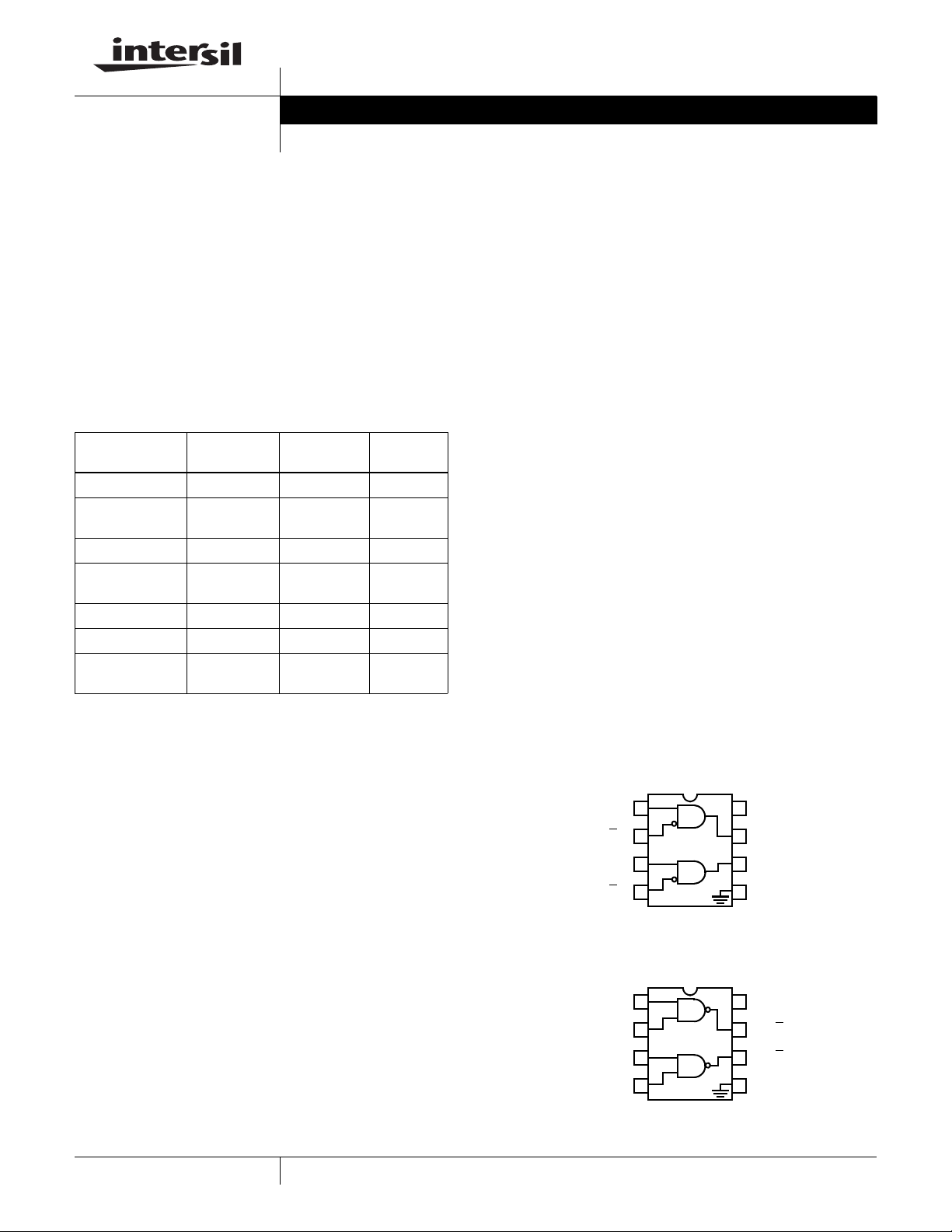
Pinouts
EL7242
(8 LD PDIP, SOIC)
TOP VIEW
A IN
B
IN
C IN
D
IN
1
2
3
4
8
7
6
5
FN7285.3
V+
OUT A
OUT B
GND
Manufactured under U.S. Patent Nos. 5,334,883, #5,341,047
1
CAUTION: These devices are sensitive to electrostatic discharge; follow proper IC Handling Procedures.
1-888-INTERSIL or 1-888-468-3774
| Intersil (and design) is a registered trademark of Intersil Americas Inc.
Copyright Intersil Americas Inc. 2003, 2005, 2008. All Rights Reserved
All other trademarks mentioned are the property of their respective owners.
EL7252
(8 LD PDIP, SOIC)
TOP VIEW
1
A IN
B IN
2
C IN
3
D IN
4
8
7
6
5
V+
OUT A
OUT B
GND
EL7242, EL7252
www.BDTIC.com/Intersil
Absolute Maximum Ratings (T
Supply (V+ to Gnd) . . . . . . . . . . . . . . . . . . . . . . . . . . . . . . . . . 16.5V
Input Pins. . . . . . . . . . . . . . . . . . . . . . . . . . -0.3V to +0.3V above V+
Combined Peak Output Current. . . . . . . . . . . . . . . . . . . . . . . . . . .4A
Storage Temperature Range . . . . . . . . . . . . . . . . . .-65°C to +150°C
Operating Conditions
Ambient Operating Temperature . . . . . . . . . . . . . . . .-40°C to +85°C
Operating Junction Temperature . . . . . . . . . . . . . . . . . . . . . .+125°C
CAUTION: Do not operate at or near the maximum ratings listed for extended periods of time. Exposure to such conditions may adversely impact product reliability and
result in failures not covered by warranty.
IMPORTANT NOTE: All parameters having Min/Max specifications are guaranteed. Typical values are for information purposes only. Unless otherwise noted, all tests
are at the specified temperature and are pulsed tests, therefore: T
DC Electrical Specifications T
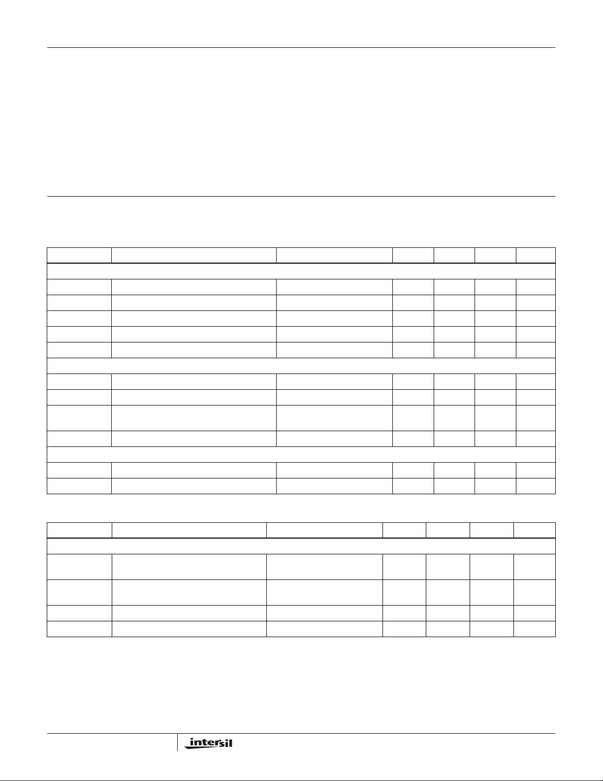
PARAMETER DESCRIPTION TEST CONDITIONS MIN TYP MAX UNITS
INPUT
V
IH
I
IH
V
IL
I
IL
V
HVS
OUTPUT
R
OH
R
OL
I
PK
I
DC
POWER SUPPLY
I
S
V
S
Logic “1' Input Voltage 2.4 V
Logic “1' Input Current @V+ 0.1 10 µA
Logic “0' Input Voltage 0.8 V
Logic “0' Input Current @0V 0.1 10 µA
Input Hysteresis 0.3 V
Pull-up Resistance I
Pull-down Resistance I
Peak Output Current Source
Continuous Output Current Source/Sink 100 mA
Power Supply Current Inputs High 1 2.5 mA
Operating Voltage 4.5 16 V
= +25°C) Thermal Information
A
Power Dissipation
8 Ld SOIC . . . . . . . . . . . . . . . . . . . . . . . . . . . . . . . . . . . . .570mW
8 Ld PDIP* . . . . . . . . . . . . . . . . . . . . . . . . . . . . . . . . . . . .1050mW
*Pb-free PDIPs can be used for through hole wave solder processing
only. They are not intended for use in Reflow solder processi ng
applications.
Pb-free reflow profile . . . . . . . . . . . . . . . . . . . . . . . . . .see link below
http://www.intersil.com/pbfree/Pb-FreeReflow.asp
= TC = T
J
= +25°C, V = 15V, unless otherwise specified.
A
A
= -100mA 3 6 Ω
OUT
= +100mA 4 6 Ω
OUT
Sink
2
2
A
AC Electrical Specifications T
PARAMETER DESCRIPTION TEST CONDITIONS MIN TYP MAX UNITS
SWITCHING CHARACTERISTICS
t
R
t
F
t
D-ON
t
D-OFF
NOTE:
1. Limits established by characterization and are not production tested.
Rise Time (Note 1) CL = 500pF
Fall Time (Note 1) CL = 500pF
Turn-On Delay Time (Note 1) 20 25 ns
Turn-Off Delay Time (Note 1) 20 25 ns
= +25°C, V = 15V, unless otherwise specified.
A
= 1000pF
C
L
= 1000pF
C
L
2
10
20
10
20
February 15, 2008
ns
ns
FN7285.3
Timing Table
www.BDTIC.com/Intersil
INPUT
INVERTED
OUTPUT
EL7242, EL7252
5V
2.5V
0
90%
10%
Standard Test Configuration
NON-INVERTED
OUTPUT
V+
INPUT
90%
10%
1
2
t
D1
3
EL7242
5
t
D2
t
F
t
R
4
7
4.7µF
TAN
OUTPUT
1000pF
LOAD
t
R
t
F
Simplified Schematic
V+
INPUT
INPUT
BUFFER
3
+
-
+
V
REF
REFERENCE AND
LEVEL SHIFTER
INVERTING
BUFFER
WITH
HYSTERESIS
LOGIC
GATE
SUPER INVERTER
OUTPUT
FN7285.3
February 15, 2008

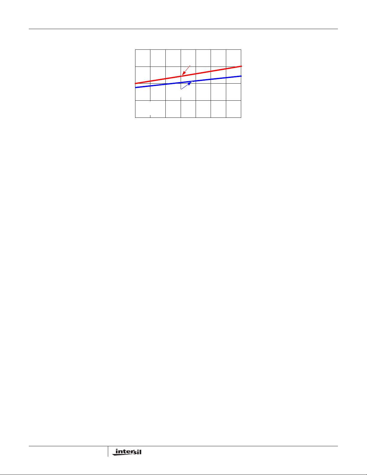
Typical Performance Curves
www.BDTIC.com/Intersil
1.0
1.05W
0.8
570mW
0.6
0.4
0.2
POWER DISSIPATION (W)
0.0
0 25 50 75 100 125 150
SO8
θ
= 175°C/W
JA
AMBIENT TEMPERATURE (°C)
FIGURE 1. MAX POWER/DERATING CURVES FIGURE 2. SWITCH THRESHOLD vs SUPPLY VOLTAGE
10
2/DIV
(mA)
0
IN
I
θ
JA
MAX T
PDIP8
= 95°C/W
= 125°C
J
EL7242, EL7252
INPUT VOLTAGE
2.0
HIGH LIMIT = 2.4V
1.8
1.6
1.4
1.2
1.0
0.0
0 5 10 15
0
-1
SINK (A)
-2
LOW LIMIT = 0.8V
SUPPLY VOLTAGE
V - SUPPLY
N-CHANNEL
HYSTERESIS
P-CHANNEL
051015
2
SOURCE (A)
1
-10
-5 0 V+ 20
V
2.5V/DIV
IN
0 5 10 15
V - SUPPLY
FIGURE 3. INPUT CURRENT vs VOLTAGE FIGURE 4. PEAK DRIVE vs SUPPLY VOLTAGE
8
7
6
5
4
3
2
SUPPL Y CURRENT (mA)
1
0
0 5 10 15
SUPPLY VOLTAGE (V)
A
CASE:
B
A
B
C
C
D
D
E
E
ALL INPUTS GND
3 INPUTS GND
2 INPUTS GND
1 INPUT GND
ALL INPUTS V+
8
6
4
2
ON-RESISTANCE (Ω)
0
PULL-UP
51015
SUPPLY VOLTAGE (V)
PULL-DOWN
FIGURE 5. QUIESCENT SUPPLY CURRENT FIGURE 6. ON-RESISTANCE vs SUPPLY VOLTAGE
MEASURED AT
100mA
4
FN7285.3
February 15, 2008

Typical Performance Curves (Continued)
www.BDTIC.com/Intersil
100
VDD = +15V
EL7242, EL7252
100
10,000pF
1000pF
10
1
SUPPLY CURRENT (mA)
0.1
10k 100k 1M 10M
VDD = +10V
VDD = +5V
CL = 1000pF
FREQUENCY (Hz)
FIGURE 7. AVERAGE SUPPLY CURRENT vs VOL TAGE AND
FREQUENCY
100
100
VDD = 10V
VDD = 10V
80
80
60
60
40
40
RISE/FALL TIME (ns)
RISE/FALL TIME (ns)
20
20
100
100
LOAD CAPACITANCE (pF)
LOAD CAPACITANCE (pF)
t
t
F
F
1000
1000
t
t
R
R
10,000
10,000
10
100pF
1
VDD = 10V
SUPPLY CURRENT (mA)
(EQUIVALENT INTERNAL
CAPACITANCE = 470pF)
0.1
10k 100k 1M 10M
FREQUENCY (Hz)
NO LOAD
FIGURE 8. AVERAGE SUPPLY CURRENT vs CAP ACITIVE
LOAD
30
20
10
RISE/FALL TIME (ns)
CL = 1000pF
0
5 7.5 10 12.5 15
t
F
t
R
SUPPLY VOLTAGE (V)
FIGURE 9. RISE/FALL TIME vs LOAD FIGURE 10. RISE/FALL TIME vs SUPPLY VOLTAGE
40
t
30
20
t
D1
DELA Y TIME (ns)
10
CL = 1000pF
0
5 7.5 10 12.5 15
SUPPLY VOLTAGE (V)
D2
30
20
10
RISE/FALL TIME (ns)
VDD = 10V
CL = 1000pF
0
-50-250 255075100125
t
F
t
R
TEMPERATURE (°C)
FIGURE 11. RISE/FALL TIME vs TEMPERATURE FIGURE 12. PROPAGATION DELAY vs SUPPLY VOLTAGE
5
FN7285.3
February 15, 2008
Typical Performance Curves (Continued)
www.BDTIC.com/Intersil
40
30
20
10
DELA Y TIME (ns)
VDD = 10V
CL = 1000pF
0
-50 -25 0 25 50 75 100 125
FIGURE 13. DELAY vs TEMPERATURE
EL7242, EL7252
t
D2
t
D1
TEMPERATURE (°C)
6
FN7285.3
February 15, 2008

Small Outline Package Family (SO)
www.BDTIC.com/Intersil
A
D
NN
(N/2)+1
EL7242, EL7252
h X 45°
PIN #1
E
C
SEATING
PLANE
0.004 C
E1
B
0.010 BM CA
I.D. MARK
1
e
0.010 BM CA
(N/2)
c
SEE DETAIL “X”
L1
H
A2
GAUGE
PLANE
A1
b
DETAIL X
L
4° ±4°
MDP0027
SMALL OUTLINE PACKAGE FAMILY (SO)
INCHES
SO16
SYMBOL
A 0.068 0.068 0.068 0.104 0.104 0.104 0.104 MAX -
A1 0.006 0.006 0.006 0.007 0.007 0.007 0.007 ±0.003 -
A2 0.057 0.057 0.057 0.092 0.092 0.092 0.092 ±0.002 -
b 0.017 0.017 0.017 0.017 0.017 0.017 0.017 ±0.003 -
c 0.009 0.009 0.009 0.011 0.011 0.011 0.011 ±0.001 -
D 0.193 0.341 0.390 0.406 0.504 0.606 0.704 ±0.004 1, 3
E 0.236 0.236 0.236 0.406 0.406 0.406 0.406 ±0.008 -
E1 0.154 0.154 0.154 0.295 0.295 0.295 0.295 ±0.004 2, 3
e 0.050 0.050 0.050 0.050 0.050 0.050 0.050 Basic -
L 0.025 0.025 0.025 0.030 0.030 0.030 0.030 ±0.009 -
L1 0.041 0.041 0.041 0.056 0.056 0.056 0.056 Basic -
h 0.013 0.013 0.013 0.020 0.020 0.020 0.020 Reference -
N 8 14 16 16 20 24 28 Reference -
NOTES:
1. Plastic or metal protrusions of 0.006” maximum per side are not included.
2. Plastic interlead protrusions of 0.010” maximum per side are not included.
3. Dimensions “D” and “E1” are measured at Datum Plane “H”.
4. Dimensioning and tolerancing per ASME Y14.5M-1994
(0.150”)
SO16 (0.300”)
(SOL-16)
SO20
(SOL-20)
SO24
(SOL-24)
SO28
(SOL-28)
TOLERANCE NOTESSO-8 SO-14
A
0.010
Rev. M 2/07
7
FN7285.3
February 15, 2008

Plastic Dual-In-Line Packages (PDIP)
www.BDTIC.com/Intersil
EL7242, EL7252
SEATING
PLANE
D
A2
A
L
L
e
b
A1
NOTE 5
c
E
eA
eB
N
PIN #1
E1
INDEX
12 N/2
MDP0031
PLASTIC DUAL-IN-LINE PACKAGE
INCHES
SYMBOL
A 0.210 0.210 0.210 0.210 0.210 MAX
A1 0.015 0.015 0.015 0.015 0.015 MIN
A2 0.130 0.130 0.130 0.130 0.130 ±0.005
b 0.018 0.018 0.018 0.018 0.018 ±0.002
b2 0.060 0.060 0.060 0.060 0.060 +0.010/-0.015
c 0.010 0.010 0.010 0.010 0.010 +0.004/-0.002
D 0.375 0.750 0.750 0.890 1.020 ±0.010 1
E 0.310 0.310 0.310 0.310 0.310 +0.015/-0.010
E1 0.250 0.250 0.250 0.250 0.250 ±0.005 2
e 0.100 0.100 0.100 0.100 0.100 Basic
eA 0.300 0.300 0.300 0.300 0.300 Basic
eB 0.345 0.345 0.345 0.345 0.345 ±0.025
L 0.125 0.125 0.125 0.125 0.125 ±0.010
N 8 14 16 18 20 Reference
NOTES:
1. Plastic or metal protrusions of 0.010” maximum per side are not included.
2. Plastic interlead protrusions of 0.010” maximum per side are not included.
3. Dimensions E and eA are measured with the leads constrained perpendicular to the seating plane.
4. Dimension eB is measured with the lead tips unconstrained.
5. 8 and 16 lead packages have half end-leads as shown.
TOLERANCE NOTESPDIP8 PDIP14 PDIP16 PDIP18 PDIP20
b2
Rev. C 2/07
All Intersil U.S. products are manufactured, assembled and tested utilizing ISO9000 quality systems.
Intersil Corporation’s quality certifications can be viewed at www.intersil.com/design/quality
Intersil products are sold by description only. Intersil Corporation reserves the right to make changes in circuit design, software and/or specifications at any time without
notice. Accordingly, the reader is cautioned to verify that data sheets are current before placing orders. Information furnished by Intersil is believed to be accurate and
reliable. However, no responsibility is assumed by Intersil or its subsidiaries for its use; nor for any infringements of patents or other rights of third parties which may result
from its use. No license is granted by implic atio n or other wise u nde r any p a tent or patent rights of Intersil or its subsidi aries.
For information regarding Intersil Corporation and its products, see www.intersil.com
8
FN7285.3
February 15, 2008
 Loading...