

®
www.BDTIC.com/Intersil
EL7232
Data Sheet December 14, 2007
Dual Channel, High Speed, High Current
Line Driver with 3-State
The EL7232 3-state drivers are particularly well suited for
ATE and microprocessor based applications. The low
quiescent power dissipation makes this part attractive in
battery applications. The 2A peak drive capability, makes the
EL7232 an excellent choice when driving high speed
capacitive lines, as well. The input circuitry provides level
shifting from TTL levels to the supply rails. The EL7232 is
available in 8 Ld PDIP and 8 Ld SO packages.
Ordering Information
PART
NUMBER
EL7232CN EL7232CN 8 Ld PDIP MDP0031
EL7232CNZ
(Note)
EL7232CS 7232CS 8 Ld SOIC MDP0027
EL7232CS-T7* 7232CS 8 Ld SOIC
EL7232CSZ
(Note)
EL7232CSZ-T7*
(Note)
EL7232CSZ-T13*
(Note)
*Please refer to TB347 for details on reel specifications.
**Pb-free PDIPs can be used for through hole wave solder
processing only. They are not intended for use in Reflow solder
processing applications.
NOTE: These Intersil Pb-free plastic packaged products employ
special Pb-free material sets; molding compounds/die attach
materials and 100% matte tin plate PLUS ANNEAL - e3 termination
finish, which is RoHS compliant and compatible with both SnPb and
Pb-free soldering operations. Intersil Pb-free products are MSL
classified at Pb-free peak reflow temperatures that meet or exceed
the Pb-free requirements of IPC/JEDEC J STD-020.
PART
MARKING PACKAGE
EL7232CN Z 8 Ld PDIP** MDP0031
T ape and Reel
7232CSZ 8 Ld SOIC
(Pb-free)
7232CSZ 8 Ld SOIC
(Pb-free)
T ape and Reel
7232CSZ 8 Ld SOIC
(Pb-free)
T ape and Reel
PKG.
DWG. #
MDP0027
MDP0027
MDP0027
MDP0027
FN7283.3
Features
• 3-State output
• 3V and 5V input compatible
• Clocking speeds up to 10MHz
• 20ns Switching/delay time
• 2A Peak drive
• Low, matched output impedance 5Ω
• Low quiescent current 2.5mA
• Wide operating voltage 4.5V to 16V
• Pb-free available (RoHS compliant)
Applications
• Parallel bus line drivers
• EPROM and PROM programming
• Motor controls
• Charge pumps
• Sampling circuits
• Pin drivers
• Bridge circuits
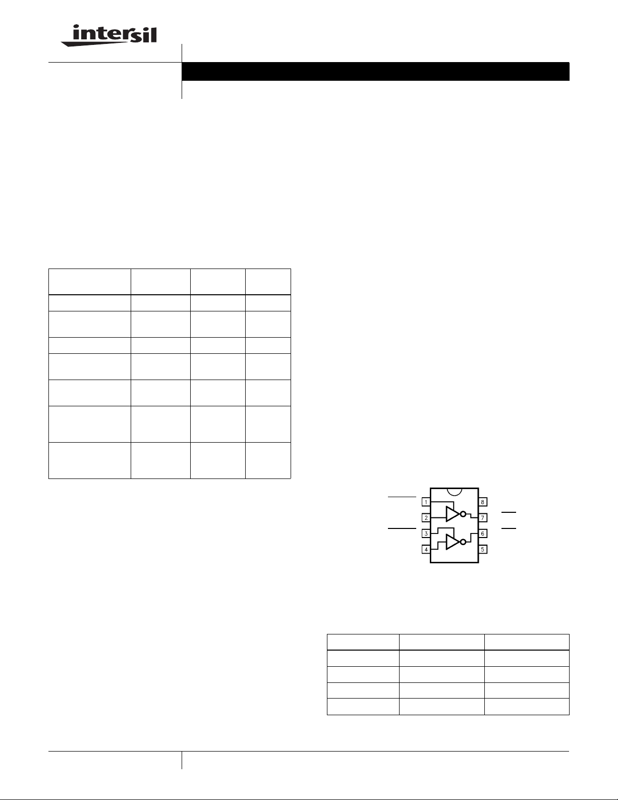
Pinout
EL7232
(8 LD PDIP, SO)
TOP VIEW
3-STATE
A IN
3-STATE
B IN
Manufactured under U.S. Patent Nos. 5,334,883, #5,341,047
V+
OUT
A
B OUT
GND
Truth Table
3-STATE INPUT OUTPUT
10 1
11 0
00Open
01Open
1
CAUTION: These devices are sensitive to electrostatic discharge; follow proper IC Handling Procedures.
1-888-INTERSIL or 1-888-468-3774
| Intersil (and design) is a registered trademark of Intersil Americas Inc.
Copyright Intersil Americas Inc. 2003, 2005-2007. All Rights Reserved
All other trademarks mentioned are the property of their respective owners.
EL7232
www.BDTIC.com/Intersil
Absolute Maximum Ratings (T
Supply (V+ to Gnd) . . . . . . . . . . . . . . . . . . . . . . . . . . . . . . . . . 16.5V
Input Pins. . . . . . . . . . . . . . . . . . . . . . . . . . -0.3V to +0.3V above V+
Combined Peak Output Current. . . . . . . . . . . . . . . . . . . . . . . . . . .4A
CAUTION: Do not operate at or near the maximum ratings listed for extended periods of time. Exposure to such conditions may adversely impact product reliability and
result in failures not covered by warranty.
IMPORTANT NOTE: All parameters having Min/Max specifications are guaranteed. Typical values are for information purposes only. Unless otherwise noted, all tests
are at the specified temperature and are pulsed tests, therefore: T
DC Electrical Specifications T
PARAMETER DESCRIPTION TEST CONDITIONS MIN TYP MAX UNITS
INPUT
V
IH
I
IH
V
IL
I
IL
V
HVS
OUTPUT
R
OH
R
OL
I
OFF
I
PK
I
DC
POWER SUPPLY
I
S
V
S
Logic “1” Input Voltage 2.4 V
Logic “1” Input Current @V+ 0.1 10 µA
Logic “0” Input Voltage 0.8 V
Logic “0” Input Current @0V 0.1 10 µA
Input Hysteresis 0.3 V
Pull-Up Resistance I
Pull-Down Resistance I
3-State Output Leakage V
Peak Output Current Source
Continuous Output Current Source/Sink 100 mA
Power Supply Current Inputs High 1 2.5 mA
Operating Voltage 4.5 16 V
= +25°C) Thermal Information
A
Operating Junction Temperature . . . . . . . . . . . . . . . . . . . . . . +125°C
Storage Temperature Range . . . . . . . . . . . . . . . . . .-65°C to +150°C
Ambient Operating Temperature . . . . . . . . . . . . . . . .-40°C to +85°C
Power Dissipation
SOIC . . . . . . . . . . . . . . . . . . . . . . . . . . . . . . . . . . . . . . . . .570mW
PDIP. . . . . . . . . . . . . . . . . . . . . . . . . . . . . . . . . . . . . . . . .1050mW
Pb-free reflow profile . . . . . . . . . . . . . . . . . . . . . . . . . .see link below
http://www.intersil.com/pbfree/Pb-FreeReflow.asp
= TC = T
J
= +25°C, V = 15V unless otherwise specified.
A
A
= -100mA 3 6 Ω
OUT
= +100mA 4 6 Ω
OUT
= V+
OUT
= 0V
V
OUT
Sink
0.2 10 µA
2.0
2.0
A
AC Electrical Specifications T
PARAMETER DESCRIPTION TEST CONDITIONS MIN TYP MAX UNITS
SWITCHING CHARACTERISTICS
t
R
t
F
t
D-ON
t
D-OFF
HIZ
HIZ
-ON
-OFF
Rise Time CL = 500pF
Fall Time CL = 500pF
Turn-On Delay Time 18 25 ns
Turn-Off Delay Time 20 25 ns
Three-State Delay, Enable 22 ns
Three-State Delay, Disable 22 ns
= +25°C, V = 15V unless otherwise specified.
A
= 1000pF
C
L
C
= 1000pF
L
2
7.5
10
10
13 20
ns
ns
FN7283.3
December 14, 2007
Timing Table
www.BDTIC.com/Intersil
Standard Test Configuration
EL7232
Simplified Schematic
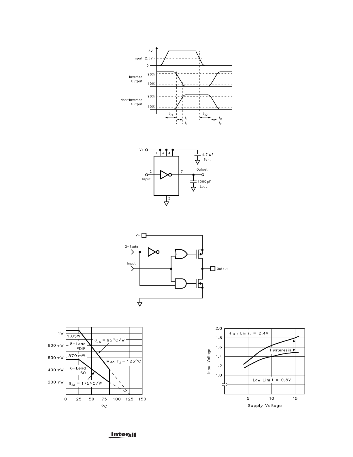
Typical Performance Curves
FIGURE 1. MAX POWER/DERATING CURVES
3
FIGURE 2. SWITCH THRESHOLD vs SUPPLY VOLTAGE
FN7283.3
December 14, 2007

Typical Performance Curves (Continued)
www.BDTIC.com/Intersil
EL7232
FIGURE 3. INPUT CURRENT vs VOLTAGE
FIGURE 5. QUIESCENT SUPPLY CURRENT
FIGURE 4. PEAK DRIVE vs SUPPLY VOLTAGE
FIGURE 6. ON-RESISTANCE vs SUPPLY VOLTAGE
FIGURE 7. AVERAGE SUPPLY CURRENT vs VOLT AGE AND
FREQUENCY
4
FIGURE 8. AVERAGE SUPPLY CURRENT vs CAPACITIVE
LOAD
FN7283.3
December 14, 2007

Typical Performance Curves (Continued)
www.BDTIC.com/Intersil
EL7232
FIGURE 9. RISE/FALL TIME vs LOAD
FIGURE 11. PROPAGATION DELAY vs SUPPLY VOLTAGE
FIGURE 10. RISE/FALL TIME vs SUPPLY VOLTAGE
FIGURE 12. RISE/FALL TIME vs TEMPERATURE
FIGURE 13. PROPAGATION DELAY vs TEMPERATURE
5
FN7283.3
December 14, 2007

Small Outline Package Family (SO)
www.BDTIC.com/Intersil
A
D
NN
(N/2)+1
EL7232
h X 45°
PIN #1
E
C
SEATING
PLANE
0.004 C
E1
B
0.010 BM CA
I.D. MARK
1
e
0.010 BM CA
(N/2)
c
SEE DETAIL “X”
L1
H
A2
GAUGE
PLANE
A1
b
DETAIL X
L
4° ±4°
MDP0027
SMALL OUTLINE PACKAGE FAMILY (SO)
INCHES
SO16
SYMBOL
A 0.068 0.068 0.068 0.104 0.104 0.104 0.104 MAX -
A1 0.006 0.006 0.006 0.007 0.007 0.007 0.007 ±0.003 -
A2 0.057 0.057 0.057 0.092 0.092 0.092 0.092 ±0.002 -
b 0.017 0.017 0.017 0.017 0.017 0.017 0.017 ±0.003 -
c 0.009 0.009 0.009 0.011 0.011 0.011 0.011 ±0.001 -
D 0.193 0.341 0.390 0.406 0.504 0.606 0.704 ±0.004 1, 3
E 0.236 0.236 0.236 0.406 0.406 0.406 0.406 ±0.008 -
E1 0.154 0.154 0.154 0.295 0.295 0.295 0.295 ±0.004 2, 3
e 0.050 0.050 0.050 0.050 0.050 0.050 0.050 Basic -
L 0.025 0.025 0.025 0.030 0.030 0.030 0.030 ±0.009 -
L1 0.041 0.041 0.041 0.056 0.056 0.056 0.056 Basic -
h 0.013 0.013 0.013 0.020 0.020 0.020 0.020 Reference -
N 8 14 16 16 20 24 28 Reference -
NOTES:
1. Plastic or metal protrusions of 0.006” maximum per side are not included.
2. Plastic interlead protrusions of 0.010” maximum per side are not included.
3. Dimensions “D” and “E1” are measured at Datum Plane “H”.
4. Dimensioning and tolerancing per ASME Y14.5M-1994
(0.150”)
SO16 (0.300”)
(SOL-16)
SO20
(SOL-20)
SO24
(SOL-24)
SO28
(SOL-28)
TOLERANCE NOTESSO-8 SO-14
A
0.010
Rev. M 2/07
6
FN7283.3
December 14, 2007

Plastic Dual-In-Line Packages (PDIP)
www.BDTIC.com/Intersil
EL7232
E
eA
eB
SEATING
PLANE
D
A2
A
L
L
e
b
A1
NOTE 5
c
MDP0031
PLASTIC DUAL-IN-LINE PACKAGE
INCHES
SYMBOL
A 0.210 0.210 0.210 0.210 0.210 MAX
A1 0.015 0.015 0.015 0.015 0.015 MIN
A2 0.130 0.130 0.130 0.130 0.130 ±0.005
b 0.018 0.018 0.018 0.018 0.018 ±0.002
b2 0.060 0.060 0.060 0.060 0.060 +0.010/-0.015
c 0.010 0.010 0.010 0.010 0.010 +0.004/-0.002
D 0.375 0.750 0.750 0.890 1.020 ±0.010 1
E 0.310 0.310 0.310 0.310 0.310 +0.015/-0.010
E1 0.250 0.250 0.250 0.250 0.250 ±0.005 2
e 0.100 0.100 0.100 0.100 0.100 Basic
eA 0.300 0.300 0.300 0.300 0.300 Basic
eB 0.345 0.345 0.345 0.345 0.345 ±0.025
L 0.125 0.125 0.125 0.125 0.125 ±0.010
N 8 14 16 18 20 Reference
NOTES:
1. Plastic or metal protrusions of 0.010” maximum per side are not included.
2. Plastic interlead protrusions of 0.010” maximum per side are not included.
3. Dimensions E and eA are measured with the leads constrained perpendicular to the seating plane.
4. Dimension eB is measured with the lead tips unconstrained.
5. 8 and 16 lead packages have half end-leads as shown.
N
PIN #1
E1
TOLERANCE NOTESPDIP8 PDIP14 PDIP16 PDIP18 PDIP20
INDEX
12 N/2
b2
Rev. C 2/07
All Intersil U.S. products are manufactured, assembled and tested utilizing ISO9000 quality systems.
Intersil Corporation’s quality certifications can be viewed at www.intersil.com/design/quality
Intersil products are sold by description only. Intersil Corporation reserves the right to make changes in circuit design, software and/or specifications at any time without
notice. Accordingly, the reader is cautioned to verify that data sheets are current before placing orders. Information furnished by Intersil is believed to be accurate and
reliable. However, no responsibility is assumed by Intersil or its subsidiaries for its use; nor for any infringements of patents or other rights of third parties which may result
from its use. No license is granted by implic atio n or other wise u nde r any p a tent or patent rights of Intersil or its subsidiaries.
For information regarding Intersil Corporation and its products, see www.intersil.com
7
FN7283.3
December 14, 2007
 Loading...