

®
www.BDTIC.com/Intersil
EL7182
Data Sheet June 15, 2006
2-Phase, High Speed CCD Driver
The EL7182 is extremely well suited for driving CCD's,
especially where high contrast imaging is desirable. The 16V
supply rating is attractive for higher voltage CCD
applications, as in color fax machines. The input is TTL and
3V compatible. The low quiescent current requirement is
advantageous in portable/battery powered systems. The
EL7182 is available in 8 Ld PDIP and 8 Ld SOIC packages.
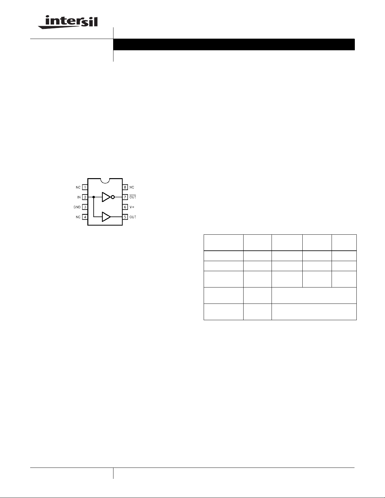
Pinout
EL7182
(8 LD PDIP, SOIC)
TOP VIEW
FN7281.1
Features
• 3V and 5V Input compatible
• Clocking speeds up to 10MHz
• Reduced clock skew
• 20ns Switching/delay time
• 2A Peak drive
• Low quiescent current
• Wide operating voltage: 4.5V–16V
• Pb-free plus anneal available (RoHS compliant)
Applications
• CCD Drivers requiring high-contrast imaging
• Differential line drivers
• Push-pull circuits
Manufactured under U.S. Patent Nos. 5,334,883, #5,341,047
Ordering Information
PART
PART NUMBER
EL7182CN EL7182CN -40 to +85 8 Ld PDIP MDP0031
EL7182CS 7182CS -40 to +85 8 Ld SOIC MDP0027
EL7182CSZ
(Note)
EL7182CSZ-T7
(Note)
EL7182CSZ-T13
(Note)
NOTE: Intersil Pb-free plus anneal products employ special Pb-free
material sets; molding compounds/die attach materials and 100%
matte tin plate termination finish, which are RoHS compliant and
compatible with both SnPb and Pb-free soldering operations. Intersil
Pb-free products are MSL classified at Pb-free peak reflow
temperatures that meet or exceed the Pb-free requirements of
IPC/JEDEC J STD-020.
MARKING
7182CSZ -40 to +85 8 Ld SOIC
7182CSZ 8 Ld SOIC (7” Tape and Reel)
7182CSZ 8 Ld SOIC (7” Tape and Reel)
TEMP.
RANGE (°C) PACKAGE
(Pb-free)
(Pb-free)
(Pb-free)
PKG.
DWG. #
MDP0027
1
CAUTION: These devices are sensitive to electrostatic discharge; follow proper IC Handling Procedures.
1-888-INTERSIL or 1-888-468-3774
| Intersil (and design) is a registered trademark of Intersil Americas Inc.
All other trademarks mentioned are the property of their respective owners.
Copyright © Intersil Americas Inc. 2003, 2006. All Rights Reserved.
EL7182
www.BDTIC.com/Intersil
Absolute Maximum Ratings (T
Supply (V+ to Gnd) . . . . . . . . . . . . . . . . . . . . . . . . . . . . . . . . . 16.5V
Input Pins. . . . . . . . . . . . . . . . . . . . . . . . . . -0.3V to +0.3V above V+
Combined Peak Output Current. . . . . . . . . . . . . . . . . . . . . . . . . . .4A
Storage Temperature Range . . . . . . . . . . . . . . . . . .-65°C to +150°C
Ambient Operating Temperature . . . . . . . . . . . . . . . .-40°C to +85°C
CAUTION: Stresses above those listed in “Absolute Maximum Ratings” may cause permanent damage to the device. This is a stress only rating and operation of the
device at these or any other conditions above those indicated in the operational sections of this specification is not implied.
IMPORTANT NOTE: All parameters having Min/Max specifications are guaranteed. Typical values are for information purposes only. Unless otherwise noted, all tests
are at the specified temperature and are pulsed tests, therefore: T
Electrical Specifications T
PARAMETER DESCRIPTION TEST CONDITIONS MIN TYP MAX UNITS
INPUT
V
IH
I
IH
V
IL
I
IL
V
HVS
OUTPUT
R
OH
R
OL
I
PK
I
DC
POWER SUPPLY
I
S
V
S
Logic “1” Input Voltage 2.4 V
Logic “1” Input Current @V+ 0.1 10 µA
Logic “0” Input Voltage 0.8 V
Logic “0” Input Current @0V 0.1 10 µA
Input Hysteresis 0.3 V
Pull-Up Resistance I
Pull-Down Resistance I
Peak Output Current Source 2 A
Continuous Output Current Source/Sink 100 mA
Power Supply Current Input High 2.5 5 mA
Operating Voltage 4.5 16 V
= 25°C)
A
= TC = T
J
= 25°C, V = 15V unless otherwise specified
A
A
= -100mA 3 6 Ω
OUT
= +100mA 4 6 Ω
OUT
Sink 2 A
Operating Junction Temperature . . . . . . . . . . . . . . . . . . . . . . . 125°C
Power Dissipation
SOIC . . . . . . . . . . . . . . . . . . . . . . . . . . . . . . . . . . . . . .570mW
PDIP . . . . . . . . . . . . . . . . . . . . . . . . . . . . . . . . . . . . . 1050mW
AC Electrical Specifications T
PARAMETER DESCRIPTION TEST CONDITIONS MIN TYP MAX UNITS
SWITCHING CHARACTERISTICS
t
R
t
F
t
D-ON
t
D-OFF
Rise Time CL = 500pF 7.5 ns
Fall Time CL = 500pF 10 ns
Turn-On Delay Time 18 25 ns
Turn-Off Delay Time 20 25 ns
2
= 25°C, V = 15V unless otherwise specified
A
CL = 1000pF 10 20 ns
= 1000pF 13 20 ns
C
L
June 15, 2006
FN7281.1
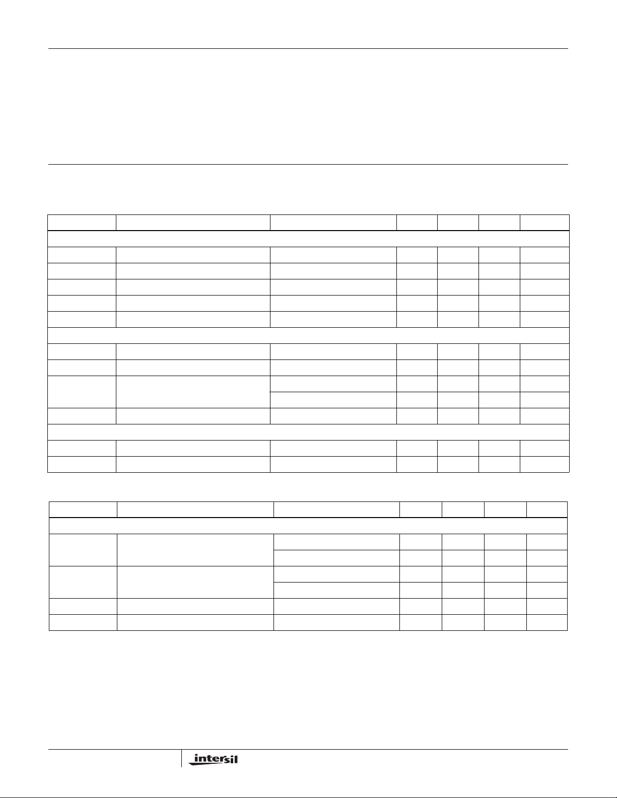
Timing Table
www.BDTIC.com/Intersil
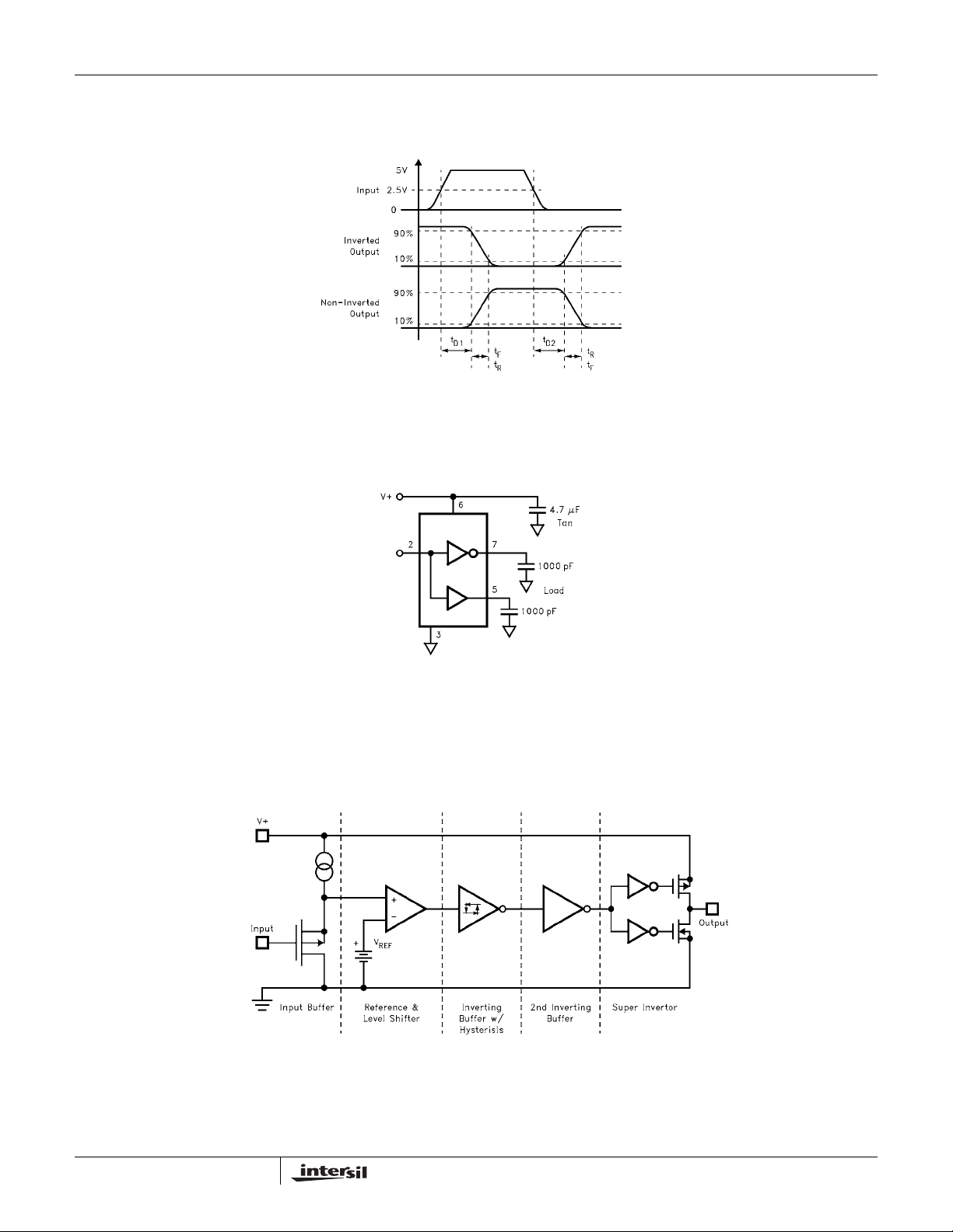
Standard Test Configuration
EL7182
Simplified Schematic
3
FN7281.1
June 15, 2006

Typical Performance Curves
www.BDTIC.com/Intersil
Max Power/Derating Curves
Input Current vs Voltage Peak Drive vs Supply Voltage
EL7182
Switch Threshold vs
Supply Voltage
Quiescent Supply Current “ON” Resistance vs Supply Voltage
CASE:
Input Level Curve
GND B
V+ D
Average Supply Current vs
Voltage and Frequency
Average Supply Current
vs Capacitive Load
4
FN7281.1
June 15, 2006

Typical Performance Curves (Continued)
www.BDTIC.com/Intersil
Rise/Fall Time vs Load Rise/Fall Time vs Supply Voltage
Rise/Fall Time vs Temperature Propagation Delay vs Supply Voltage
EL7182
Delay Time vs Temperature
5
FN7281.1
June 15, 2006

Small Outline Package Family (SO)
www.BDTIC.com/Intersil
A
D
NN
(N/2)+1
EL7182
h X 45°
PIN #1
E
C
SEATING
PLANE
0.004 C
E1
B
0.010 BM CA
I.D. MARK
1
e
0.010 BM CA
(N/2)
c
SEE DETAIL “X”
L1
H
A2
GAUGE
PLANE
A1
b
DETAIL X
L
4° ±4°
MDP0027
SMALL OUTLINE PACKAGE FAMILY (SO)
SYMBOL SO-8 SO-14
A 0.068 0.068 0.068 0.104 0.104 0.104 0.104 MAX -
A1 0.006 0.006 0.006 0.007 0.007 0.007 0.007 ±0.003 -
A2 0.057 0.057 0.057 0.092 0.092 0.092 0.092 ±0.002 -
b 0.017 0.017 0.017 0.017 0.017 0.017 0.017 ±0.003 -
c 0.009 0.009 0.009 0.011 0.011 0.011 0.011 ±0.001 -
D 0.193 0.341 0.390 0.406 0.504 0.606 0.704 ±0.004 1, 3
E 0.236 0.236 0.236 0.406 0.406 0.406 0.406 ±0.008 -
E1 0.154 0.154 0.154 0.295 0.295 0.295 0.295 ±0.004 2, 3
e 0.050 0.050 0.050 0.050 0.050 0.050 0.050 Basic -
L 0.025 0.025 0.025 0.030 0.030 0.030 0.030 ±0.009 -
L1 0.041 0.041 0.041 0.056 0.056 0.056 0.056 Basic -
h 0.013 0.013 0.013 0.020 0.020 0.020 0.020 Reference -
N 8 14 16 16 20 24 28 Reference -
NOTES:
1. Plastic or metal protrusions of 0.006” maximum per side are not included.
2. Plastic interlead protrusions of 0.010” maximum per side are not included.
3. Dimensions “D” and “E1” are measured at Datum Plane “H”.
4. Dimensioning and tolerancing per ASME Y14.5M-1994
SO16
(0.150”)
SO16 (0.300”)
(SOL-16)
SO20
(SOL-20)
SO24
(SOL-24)
SO28
(SOL-28) TOLERANCE NOTES
A
0.010
Rev. L 2/01
6
FN7281.1
June 15, 2006

Plastic Dual-In-Line Packages (PDIP)
www.BDTIC.com/Intersil
EL7182
D
A2
SEATING
PLANE
L
L
e
MDP0031
PLASTIC DUAL-IN-LINE PACKAGE
SYMBOL PDIP8 PDIP14 PDIP16 PDIP18 PDIP20 TOLERANCE NOTES
A 0.210 0.210 0.210 0.210 0.210 MAX
A1 0.015 0.015 0.015 0.015 0.015 MIN
A2 0.130 0.130 0.130 0.130 0.130 ±0.005
b 0.018 0.018 0.018 0.018 0.018 ±0.002
b2 0.060 0.060 0.060 0.060 0.060 +0.010/-0.015
c 0.010 0.010 0.010 0.010 0.010 +0.004/-0.002
D 0.375 0.750 0.750 0.890 1.020 ±0.010 1
E 0.310 0.310 0.310 0.310 0.310 +0.015/-0.010
E1 0.250 0.250 0.250 0.250 0.250 ±0.005 2
e 0.100 0.100 0.100 0.100 0.100 Basic
eA 0.300 0.300 0.300 0.300 0.300 Basic
eB 0.345 0.345 0.345 0.345 0.345 ±0.025
L 0.125 0.125 0.125 0.125 0.125 ±0.010
N 8 14 16 18 20 Reference
b
A
c
A1
NOTE 5
E
eA
eB
N
PIN #1
E1
INDEX
12 N/2
b2
Rev. B 2/99
NOTES:
1. Plastic or metal protrusions of 0.010” maximum per side are not included.
2. Plastic interlead protrusions of 0.010” maximum per side are not included.
3. Dimensions E and eA are measured with the leads constrained perpendicular to the seating plane.
4. Dimension eB is measured with the lead tips unconstrained.
5. 8 and 16 lead packages have half end-leads as shown.
All Intersil U.S. products are manufactured, assembled and tested utilizing ISO9000 quality systems.
Intersil Corporation’s quality certifications can be viewed at www.intersil.com/design/quality
Intersil products are sold by description only. Intersil Corporation reserves the right to make changes in circuit design, software and/or specifications at any time without
notice. Accordingly, the reader is cautioned to verify that data sheets are current before placing orders. Information furnished by Intersil is believed to be accurate and
reliable. However, no responsibility is assumed by Intersil or its subsidiaries for its use; nor for any infringements of patents or other rights of third parties which may result
from its use. No license is granted by implic atio n or other wise u nde r any p a tent or patent rights of Intersil or its subsidiaries.
For information regarding Intersil Corporation and its products, see www.intersil.com
7
FN7281.1
June 15, 2006
 Loading...