

®
www.BDTIC.com/Intersil
EL7158
Data Sheet May 14, 2007
Ultra-High Current Pin Driver
The EL7158 high performance pin
driver with three-state is suited to
many ATE and level-shifting
applications. The 12A peak drive capability makes this part
an excellent choice when driving high capacitance loads.
The output pin OUT is connected to input pins VH or VL
respectively, depending on the status of the IN pin. When the
OE pin is active low, the output is placed in the three-state
mode. The isolation of the output FETs from the power
supplies enables VH and VL to be set independently,
enabling level-shifting to be implemented. Related to the
EL7155, the EL7158 adds a lower supply pin VS- and makes
VL an isolated and independent input. This feature adds
applications flexibility and improves switching response due
to the increased enhancement of the output FETs.
This pin driver has improved performance over existing pin
drivers. It is specifically designed to operate at voltages
down to 0V across the switch elements while maintaining
good speed and ON-resistance characteristics.
Available in the 8 Ld SOIC package, the EL7158 is specified
for operation over the full -40°C to +85°C temperature range.
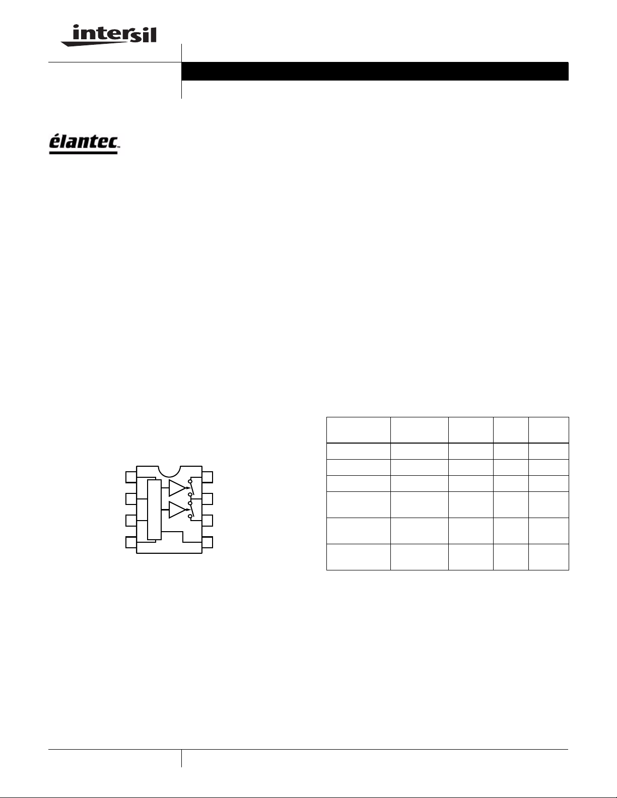
Pinout
EL7158
(8 LD SOIC)
TOP VIEW
VS+
OE
GND
1
L
2
O
G
IN
I
3
C
4
8
VH
OUT
7
VL
6
VS-
5
FN7349.2
Features
• Clocking speeds up to 40MHz
• 12ns t
at 2000pF C
R/tF
LOAD
• 0.2ns rise and fall times mismatch
• 0.5ns t
ON-tOFF
prop delay mismatch
• 3.5pF typical input capacitance
• 12A peak drive
• Low ON-resistance of 0.5Ω
• High capacitive drive capability
• Operates from 4.5V to 12V
• Pb-free plus anneal available (RoHS compliant)
Applications
• ATE/burn-in testers
• Level shifting
•IGBT drivers
• CCD drivers
Ordering Information
PART
NUMBER
EL7158IS 7158IS 8 Ld SOIC - MDP0027
EL7158IS-T7 7158IS 8 Ld SOIC 7” MDP0027
EL7158IS-T13 7158IS 8 Ld SOIC 13” MDP0027
EL7158ISZ
(Note)
EL7158ISZ-T7
(Note)
EL7158ISZ-T13
(Note)
NOTE: Intersil Pb-free products employ special Pb-free material
sets; molding compounds/die attach materials and 100% matte tin
plate termination finish, which is compatible with both SnPb and
Pb-free soldering operations. Intersil Pb-free products are MSL
classified at Pb-free peak reflow temperatures that meet or exceed
the Pb-free requirements of IPC/JEDEC J Std-020B.
PART
MARKING PACKAGE
7158ISZ 8 Ld SOIC
(Pb-free)
7158ISZ 8 Ld SOIC
(Pb-free)
7158ISZ 8 Ld SOIC
(Pb-free)
TAPE &
REEL
7” MDP0027
13” MDP0027
PKG.
DWG. #
- MDP0027
1
Copyright © Intersil Americas Inc. 2003, 2004, 2007. All Rights Reserved. Elantec is a registered trademark of Elantec Semiconductor, Inc.
CAUTION: These devices are sensitive to electrostatic discharge; follow proper IC Handling Procedures.
1-888-INTERSIL or 1-888-468-3774
| Intersil (and design) is a registered trademark of Intersil Americas Inc.
All other trademarks mentioned are the property of their respective owners.
EL7158
www.BDTIC.com/Intersil
Absolute Maximum Ratings (T
Supply Voltage (VS+ to VS-) . . . . . . . . . . . . . . . . . . . . . . . . . . .+18V
Input Voltage . . . . . . . . . . . . . . . . . . . . . . . . . . .V
Continuous Output Current . . . . . . . . . . . . . . . . . . . . . . . . . . 500mA
CAUTION: Stresses above those listed in “Absolute Maximum Ratings” may cause permanent damage to the device. This is a stress only rating and operation of the
device at these or any other conditions above those indicated in the operational sections of this specification is not implied.
IMPORTANT NOTE: All parameters having Min/Max specifications are guaranteed. Typical values are for information purposes only. Unless otherwise noted, all tests
are at the specified temperature and are pulsed tests, therefore: TJ = TC = T
Electrical Specifications V
PARAMETER DESCRIPTION CONDITION MIN TYP MAX UNIT
INPUT
V
IH
I
IH
V
IL
I
IL
C
IN
R
IN
OUTPUT
R
OVH
R
OVL
I
OUT
I
PK
I
DC
POWER SUPPLY
I
S
I
VH
SWITCHING CHARACTERISTICS
t
R
t
F
t
RFΔ
t
d-1
t
d-2
t
dΔ
t
d-3
t
d-4
SR+ V
SR- V
Logic ‘1’ Input Voltage 2.4 V
Logic ‘1’ Input Current VIH = VS+0.110µA
Logic ‘0’ Input Voltage 0.8 V
Logic ‘0’ Input Current VIL = 0V 0.1 10 µA
Input Capacitance 3.5 pF
Input Resistance 50 MΩ
ON-Resistance VH to OUT I
ON-Resistance VL to OUT I
Output Leakage Current OE = 0V, OUT = VH/V
Peak Output Current
(linear resistive operation)
Continuous Output Current Source/Sink 500 mA
Power Supply Current Inputs = VS+1.33mA
Off Leakage at VH and V
Rise Time CL = 2000pF 12.0 ns
Fall Time CL = 2000pF 12.2 ns
tR, tF Mismatch CL = 2000pF 0.2 ns
Turn-Off Delay Time CL = 2000pF 22.5 ns
Turn-On Delay Time CL = 2000pF 22.0 ns
t
Mismatch CL = 2000pF 0.5 ns
d-1-td-2
Three-State Delay Enable 22 ns
Three-State Delay Disable 22 ns
+ Slew Rate R
OUT
- Slew Rate R
OUT
= +25°C) Thermal Information
A
- -0.3V, VS +0.3V
S
A
+ = +12V, VH = +12V, VL = 0V, VS- = 0V, TA = +25°C, unless otherwise specified.
S
= -500mA 0.5 1 Ω
OUT
= +500mA 0.5 1 Ω
OUT
Source 12 A
Sink 12 A
L
VH, VL = 0V 4 10 µA
= 6Ω 800 V/µs
LOAD
= 6Ω 800 V/µs
LOAD
Storage Temperature Range . . . . . . . . . . . . . . . . . .-65°C to +15 0°C
Ambient operating Temperature . . . . . . . . . . . . . . . .-40°C to +85°C
Operating Junction Temperature . . . . . . . . . . . . . . . . . . . . . . +125°C
Power Dissipation . . . . . . . . . . . . . . . . . . . . . . . . . . . . . . see curves
Pb-free reflow profile . . . . . . . . . . . . . . . . . . . . . . . . . .see link below
http://www.intersil.com/pbfree/Pb-FreeReflow.asp
L
0.1 10 µA
2
FN7349.2
May 14, 2007
EL7158
www.BDTIC.com/Intersil
Electrical Specifications V
PARAMETER DESCRIPTION CONDITION MIN TYP MAX UNIT
INPUT
V
IH
I
IH
V
IL
I
IL
C
IN
R
IN
OUTPUT
R
OVH
R
OVL
I
OUT
I
PK
I
DC
POWER SUPPLY
I
S
V
H
SWITCHING CHARACTERISTICS
t
R
t
F
t
RFΔ
t
d-1
t
d-2
t
dΔ
t
d-3
t
d-4
SR+ V
SR- V
Logic ‘1’ Input Voltage 2.0 V
Logic ‘1’ Input Current VIH = VS+0.110µA
Logic ‘0’ Input Voltage 0.8 V
Logic ‘0’ Input Current VIL = 0V 0.1 10 µA
Input Capacitance 3.5 pF
Input Resistance 50 MΩ
ON-Resistance VH to OUT I
ON-Resistance VL to OUT I
Output Leakage Current OE = 0V, OUT = VH/V
Peak Output Current
(linear resistive operation)
Continuous Output Current Source/Sink 500 mA
Power Supply Current Inputs = VS+12.5mA
Off Leakage at VH and V
Rise Time CL = 2000pF 11 ns
Fall Time CL = 2000pF 11 ns
tR, tF Mismatch CL = 2000pF 0 ns
Turn-Off Delay Time CL = 2000pF 20.5 ns
Turn-On Delay Time CL = 2000pF 20.0 ns
t
Mismatch CL = 2000pF 0.5 ns
d-1-td-2
Three-State Delay Enable 20 ns
Three-State Delay Disable 20 ns
+ Slew Rate R
OUT
- Slew Rate R
OUT
+ = +12V, VH = +1.2V, VL = 0V, VS- = 0V, TA = +25°C, unless otherwise specified. (Continued)
S
= -500mA 0.5 1 Ω
OUT
= +500mA 0.5 1 Ω
OUT
L
Source 1.2 A
Sink 1.2 A
L
VH, VL = 0V 4 10 µA
= 6Ω 80 V/µs
LOAD
= 6Ω 80 V/µs
LOAD
0.1 10 µA
3
FN7349.2
May 14, 2007

Typical Performance Curves
www.BDTIC.com/Intersil
EL7158
T = +25°C
1.8
1.6
1.4
1.2
INPUT VOLTAGE (V)
1.0
HIGH THRESHOLD
HYSTERESIS
LOW THRESHOLD
12510
SUPPLY VOLTAGE (V)
T = +25°C
2.0
1.6
1.2
ALL INPUTS = GND
0.8
SUPPLY CURRENT (mA)
0.4
0
5
SUPPLY VOLTAGE (V)
ALL INPUTS = VS+
10
12
FIGURE 1. INPUT THRESHOLD vs SUPPLY VOLTAGE FIGURE 2. QUIESCENT SUPPLY CURRENT vs SUPPLY
VOLTAGE
I
= 500mA, T = +25°C, VS+ = VH, VS- = VL = 0V
OUT
0.8
0.7
0.6
VH TO V
OUT
CL = 2000pF, T = +25°C, VS+ = VH, VS- = VL = 0V
15
14
t
R
13
0.5
“ON” RESISTANCE (Ω)
0.4
V
TO V
OUT
L
7.5 12.5510
SUPPLY VOLTAGE (V)
FIGURE 3. “ON”-RESISTANCE vs SUPPLY VOLTAGE (V
CL = 2000pF, VS+ = VH = 12V, VS- = VL = 0V
18
16
t
t
R
r
14
12
RISE/FALL TIME (ns)
10
8
-50
0
TEMPERATURE (°C)
t
R
50
100
150
+) FIGURE 4. RISE/FALL TIME vs SUPPLY VOLTAGE
S
12
RISE/FALL TIME (ns)
11
30
28
26
24
DELAY TIME (ns)
22
20
t
F
6 8 10 12
71159
SUPPLY VOLTAGE (V)
CL = 2000pF, T = +25°C, VS+ = VH = 12V,
- = VL = 0V
V
S
t
d2
711596 8 10 12
SUPPLY VOLTAGE (V)
t
d1
FIGURE 5. RISE/FALL TIME vs TEMPERATURE FIGURE 6. PROPAGATION DELAY vs SUPPLY VOLTAGE
4
FN7349.2
May 14, 2007

Typical Performance Curves (Continued)
www.BDTIC.com/Intersil
EL7158
CL = 2000pF, VS+ = VH = 12V, VS- = VL = 0V
26
DELA Y TIME (ns)
24
22
20
18
-25 25 75 100
t
D1
0125-50 50
TEMPERATURE (°C)
t
D2
VS+ = +12V, T = +25°C
70
60
50
40
30
20
RISE/FALL TIME (ns)
10
0
100 1k
LOAD CAPACITANCE (pF)
t
F
t
R
10k
FIGURE 7. PROPAGATION DELAY vs TEMPERATURE FIGURE 8. RISE/FALL TIME vs LOAD CAPACITANCE
+ = VH = 12V, VS- = VL = 0V, T = +25 °C, f = 20kHz
V
S
5
4
3
= 1000pF, T = +25°C
C
L
100
10
VS+=12V
2
1
SUPPL Y CURRENT (mA)
0
100 1k 10k
LOAD CAPACITANCE (pF)
SUPPL Y CURRENT (mA)
1.0
VS+=5V
0.1
FREQUENCY (Hz)
VS+=10V
1M 10M10k 100k
FIGURE 9. SUPPLY CURRENT vs LOAD CAPACITANCE FIGURE 10. SUPPLY CURRENT vs FREQUENCY
JEDEC JESD51-3 LOW EFFECTIVE THERMAL
CONDUCTIVITY TEST BOARD
1.0
0.9
0.8
0.7
625mW
0.6
0.5
0.4
0.3
0.2
POWER DISSIPATION (W)
0.1
0
0 255075100 150
S
O
θ
I
C
J
A
8
=
1
6
0
°
C
/
W
AMBIENT TEMPERATURE (°C)
12585
JEDEC JESD51-7 HIGH EFFECTIVE THERMAL
CONDUCTIVITY TEST BOARD
1.4
1.2
1.0
909mW
0.8
0.6
0.4
POWER DISSIPATION (W)
0.2
0
0 255075100 150
S
θ
O
JA
I
C
=
8
1
1
0
°
C/
W
AMBIENT TEMPERATURE (°C)
12585
FIGURE 11. P ACKAGE POWER DISSIP ATION vs AMBIENT
FIGURE 12. PACKAGE POWER DISSIP A TION vs AMBIENT
TEMPERATURE
5
TEMPERATURE
FN7349.2
May 14, 2007

EL7158
www.BDTIC.com/Intersil
TABLE 1. TRUTH TABLE
OE IN OUT
0 0 Three-State
0 1 Three-State
10V
11V
INPUT
INVERTED
OUTPUT
2.5V
0
90%
10%
5V
H
L
t
d1
TABLE 2. OPERATING VOLTAGE RANGE
PIN MIN MAX
- to GND -5 0
V
S
+ to VS-5 18
V
S
to V
V
H
L
+ to V
V
S
H
+ to GND 5 12
V
S
to VS-0 12
V
L
Three-State Output V
t
d2
t
F
t
R
012
012
L
V
H
V
VS+
FIGURE 13. TIMING DIAGRAM
V
H
+
S
0.1µF4.7µF
10kΩ
OE
IN
GND
1
L
O
2
G
I
3
C
4
EL7158
8
7
6
5
0.1µF
2000pF
0.1µF 4.7µF
0.1µF 4.7µF
4.7µF
-
-
OUT
V
L
VS-
FIGURE 14. STANDARD TEST CONFIGURATION
6
FN7349.2
May 14, 2007

EL7158
www.BDTIC.com/Intersil
Pin Descriptions
PIN NAME FUNCTION EQUIVALENT CIRCUIT
1 VS+ Positive Supply Voltage
2 OE Output Enable
3 IN Input Reference Circuit 1
4 GND Ground
5 VS- Negative Supply Voltage
6 VL Lower Output Voltage
7 OUT Output
INPUT
VS+
V
VS-
-
S
Circuit 1
V
H
+
V
S
8 VH High Output Voltage
VS+
GND
V
IN
-
S
LEVEL
SHIFTER
OE
THREE-
STATE
CONTROL
V
OUT
V
-
S
VS-
V
L
Circuit 2
V
H
OUT
V
L
FIGURE 15. BLOCK DIAGRAM
7
FN7349.2
May 14, 2007

EL7158
www.BDTIC.com/Intersil
Applications Information
Product Description
The EL7158 is a high performance 40MHz pin driver. It
contains two analog switches connecting VH and VL to OUT .
Depending on the value of the IN pin, one of the two
switches will be closed and the other switch open. An output
enable (OE) is also supplied which opens both switches
simultaneously.
Due to the topology of t he EL7158, both the VH and VL pins
can be connected to any voltage between the VS+ and VSpins, but VH must be greater than VL in order to prevent
turning on the body diode at the output stage.
Three-State Operation
When the OE pin is low, the output is three-state (floating).
The output voltage is the parasitic capacitance’s voltage. It
can be any voltage between VH and VL, depending on the
previous state. At three-state, the output voltage can be
pushed to any voltage between VH and V
voltage can’t be pushed higher than VH or lower than VL
since the body diode at the output stage will turn on.
Supply Voltage Ra nge and Input Compatibility
The EL7158 is designed for operation on supplies from 5V to
18V (4.5V to 18V maximum). Table 2 shows the
specifications for the relationship between the VS+, VS-, VH,
VL, and GND pins.
All input pins are compatible with both 3V and 5V CMOS
signals. With a positive supply (V
+) of 5V, the EL7158 is
S
also compatible with TTL inputs.
Power Supply Bypassing
When using the EL7158, it is very important to use adequate
power supply bypassing. The high switching currents
developed by the EL7158 necessitate the use of a bypass
capacitor between the supplies (V
pins. It is recommended that a 2.2µF tantalum capacitor be
used in parallel with a 0.1µF low-inductance ceramic MLC
capacitor. These should be placed as close to the supply
pins as possible. It is also recommended that the V
pins have some level of bypassing, especially if the EL7158
is driving highly capacitive loads.
S
. The output
L
+ and VS-) and GND
and VL
H
Power Dissipation Calculation
When switching at high speeds, or driving heavy loads, the
EL7158 drive capability is limited by the rise in die
temperature brought about by internal power dissipation. For
reliable operation die temperature must be kept below
T
(+125°C). It is necessary to calculate the power
JMAX
dissipation for a given application prior to selecting the
package type.
Power dissipation may be calculated:
PD VS( IS) C
( V
INT
2
f) CL( V
S
where:
V
is the total power supply to the EL7158 (from VS+ to
S
GND)
V
is the swing on the output (VH - VL)
OUT
is the load capacitance
C
L
is the internal load capacitance (100pF max)
C
INT
is the quiescent supply current (3mA max)
I
S
f is frequency
Having obtained the application’s power dissipation, a
maximum package thermal coefficient may be determined,
to maintain the internal die temperature below T
T
–
JMAXTMAX
-----------------------------------------
=
θ
JA
PD
where:
T
is the maximum junction temperature (+125°C)
JMAX
is the maximum operating temperature
T
MAX
PD is the power dissipation calculated above
thermal resistance on junction to ambient
θ
JA
is 160°C/W for the SOIC8 package when using a
θ
JA
standard JEDEC JESD51-3 single-layer test board. If T
is greater than +125°C when calculated using Equation 2 ,
then one of the following actions must be taken:
Reduce θ
the system by designing more heat-sinking
JA
into the PCB (as compared to the standard JEDEC
JESD51-3)
OUT
2
f)××+××+×=
JMAX
(EQ. 1)
:
(EQ. 2)
JMAX
De-rate the application either by reducing the switching
frequency, the capacitive load, or the maximum operating
(ambient) temperature (T
All Intersil U.S. products are manufactured, assembled and tested utilizing ISO9000 quality systems.
Intersil Corporation’s quality certifications can be viewed at www.intersil.com/design/quality
Intersil products are sold by description only. Intersil Corporation reserves the right to make changes in circuit design, software and/or specifications at any time without
notice. Accordingly, the reader is cautioned to verify that data sheets are current before placing orders. Information furnished by Intersil is believed to be accurate and
reliable. However, no responsibility is assumed by Intersil or its subsidiaries for its use; nor for any infringements of patents or other rights of third parties which may result
from its use. No license is granted by implic atio n or other wise u nde r any p a tent or patent rights of Intersil or it s sub s idiari es.
For information regarding Intersil Corporation and its products, see www.intersil.com
8
MAX
)
FN7349.2
May 14, 2007

Small Outline Package Family (SO)
www.BDTIC.com/Intersil
A
D
NN
(N/2)+1
EL7158
h X 45°
PIN #1
E
C
SEATING
PLANE
0.004 C
E1
B
0.010 BM CA
I.D. MARK
1
e
0.010 BM CA
(N/2)
c
SEE DETAIL “X”
L1
H
A2
GAUGE
PLANE
A1
b
DETAIL X
L
4° ±4°
MDP0027
SMALL OUTLINE PACKAGE FAMILY (SO)
INCHES
SO16
SYMBOL
A 0.068 0.068 0.068 0.104 0.104 0.104 0.104 MAX -
A1 0.006 0.006 0.006 0.007 0.007 0.007 0.007 ±0.003 -
A2 0.057 0.057 0.057 0.092 0.092 0.092 0.092 ±0.002 -
b 0.017 0.017 0.017 0.017 0.017 0.017 0.017 ±0.003 -
c 0.009 0.009 0.009 0.011 0.011 0.011 0.011 ±0.001 -
D 0.193 0.341 0.390 0.406 0.504 0.606 0.704 ±0.004 1, 3
E 0.236 0.236 0.236 0.406 0.406 0.406 0.406 ±0.008 -
E1 0.154 0.154 0.154 0.295 0.295 0.295 0.295 ±0.004 2, 3
e 0.050 0.050 0.050 0.050 0.050 0.050 0.050 Basic -
L 0.025 0.025 0.025 0.030 0.030 0.030 0.030 ±0.009 -
L1 0.041 0.041 0.041 0.056 0.056 0.056 0.056 Basic -
h 0.013 0.013 0.013 0.020 0.020 0.020 0.020 Reference -
N 8 14 16 16 20 24 28 Reference -
NOTES:
1. Plastic or metal protrusions of 0.006” maximum per side are not included.
2. Plastic interlead protrusions of 0.010” maximum per side are not included.
3. Dimensions “D” and “E1” are measured at Datum Plane “H”.
4. Dimensioning and tolerancing per ASME Y14.5M-1994
(0.150”)
SO16 (0.300”)
(SOL-16)
SO20
(SOL-20)
SO24
(SOL-24)
SO28
(SOL-28)
TOLERANCE NOTESSO-8 SO-14
A
0.010
Rev. M 2/07
9
FN7349.2
May 14, 2007
 Loading...