

查询EL5611供应商
®
EL5611, EL5811
Data Sheet May 26, 2004
60MHz Rail-to-Rail Input-Output V
COM
Amplifiers
The EL5611 and EL5811 are low
power, high voltage rail-to-rail inputoutput amplifiers targeted primarily at
V
applications in TFT-LCD displays. The EL5611
COM
contains six amplifiers, and the EL5811 contains eight
amplifier s . Operating on supplies ranging from 5V to 15V,
while consuming only 2.5mA per am plifier, the EL5611 and
EL5811 have a bandwidth of 60MHz (-3dB). They also
provide common mode input ability beyond the supply rail s,
as well as rail-to-rail output capability. This enables these
amplifiers to offer maximum dynamic range at any supply
voltage.
The EL5611 and EL5811 also feature fast slewing and
settling times, as well as a high output drive capability of
65mA (sink and source). In addition to V
applications,
COM
these features make these amplifiers ideal for high speed
filtering and signal conditioning application. Other
applications include battery power, portable devices, and
anywhere low power consumption is important.
The EL5611 is available in 8-pin MSOP and 8-pin HMSOP
packages. The EL5811 is available in space-saving 28-pin
HTSSOP packages.These amplifiers operate over a
temperature range of -40°C to +85°C.
Ordering Information
PART NUMBER PACKAGE
EL5611IRE 24-Pin HTSSOP - MDP0048
EL5611IRE-T7 24-Pin HTSSOP 7” MDP0048
EL5611IRE-T13 24-Pin HTSSOP 13” MDP0048
EL5811IRE 28-Pin HTSSOP - MDP0048
EL5811IRE-T7 28-Pin HTSSOP 7” MDP0048
EL5811IRE-T13 28-Pin HTSSOP 13” MDP0048
EL5811IREZ
(Note)
EL5811IREZ-T7
(Note)
EL5811IREZ-T13
(Note)
NOTE: Intersil Pb-free products employ spec ial Pb-free material
sets; molding compounds/die attach materials and 100% matte tin
plate termination finish, which is compatible with both SnPb and
Pb-free soldering operations. Intersil Pb-free products are MSL
classified at Pb-free peak reflow temperatures that meet or exceed
the Pb-free requirements of IPC/JEDEC J Std-020B.
28-Pin HTSSOP
(Pb-Free)
28-Pin HTSSOP
(Pb-Free)
28-Pin HTSSOP
(Pb-Free)
TAPE &
REEL PKG. DWG. #
- MDP0048
7” MDP0048
13” MDP0048
Features
• 60MHz -3dB bandwidth
• Supply voltage = 4.5V to 16.5V
• Low supply current (per amplifier) = 2.5mA
• High slew rate = 75V/µs
• Unity-gain stable
• Beyond the rails input capability
• Rail-to-rail output swing
• ±180mA output short current
• Pb-free packaging available
Applications
• TFT-LCD panels
•V
• Drivers for A-to-D converters
• Data acquisition
• Video processing
• Audio processing
• Active filters
• Test equipment
• Battery-powered applications
• Portable equipment
COM
amplifiers
FN7355
1
Copyright © Intersil Americas Inc. 2004. All Rights Reserved. Elantec is a registered trademark of Elantec Semiconductor, Inc.
CAUTION: These devices are sensitive to electrostatic discharge; follow proper IC Handling Procedures.
1-888-INTERSIL or 321-724-7143
| Intersil (and design) is a registered trademark of Intersil Americas Inc.
All other trademarks mentioned are the property of their respective owners.
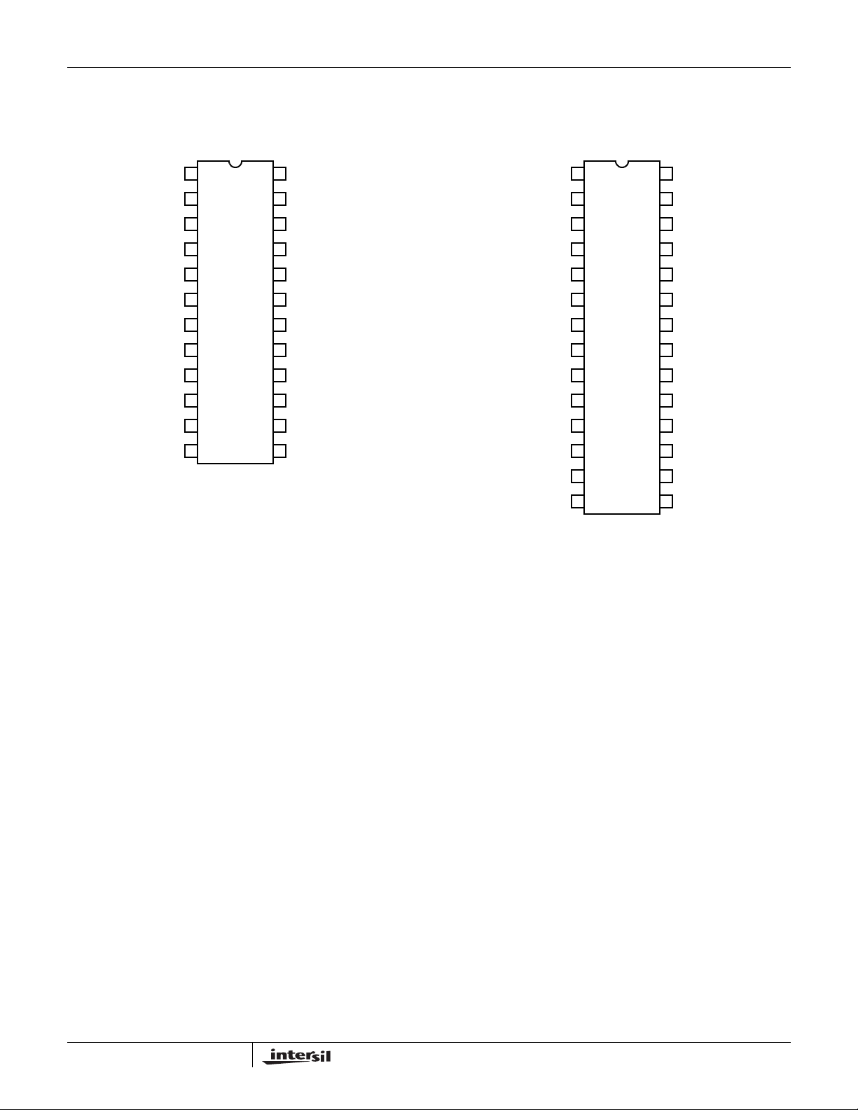
Pinouts
EL5611
(24-PIN HTSSOP)
TOP VIEW
EL5611, EL5811
EL5811
(28-PIN HTSSOP)
TOP VIEW
VOUTA
VINA-
VINA+
VSS
VOUTB
VINB-
VINB+
VDD
VINC+
VINC-
VOUTC
NC
1
2
3
4
5
6
7
8
9
10
11
12
24
23
22
21
20
19
18
17
16
15
14
13
VDD
VOUTF
VINF-
VINF+
VOUTE
VINE-
VINE+
VSS
VOUTD+
VOUTD-
VOUTD
NC
VDD
1
VINA+
2
VINA-
3
VOUTA
VOUTD
4
VOUTB
5
VINB-
6
VINB+
7
VINC+
8 21
VINC-
9
VOUTC
10
11
VIND-
12
VIND+
13
VDD
14 15
28
27
26
25
24
23
22
20
19
18
17
16
VINH+
VINH-
VOUTH
VOUTG
VING-
VING+
VSS
VSS
VINF+
VINF-
VOUTF
VOUTE
VINE-
VINE+
2
EL5611, EL5811
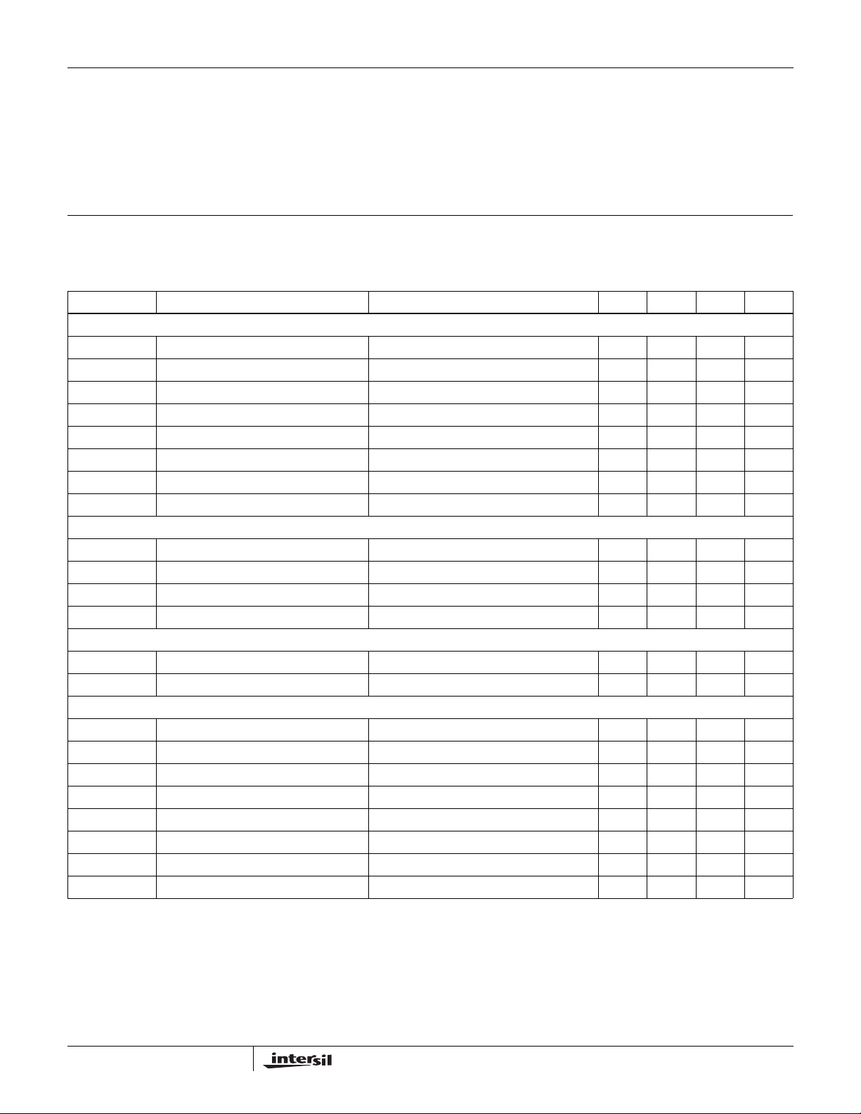
Absolute Maximum Ratings (T
Supply Voltage between V
Input Voltage . . . . . . . . . . . . . . . . . . . . . . . . . . V
Maximum Continuous Output Current . . . . . . . . . . . . . . . . . . . 65mA
+ and VS-. . . . . . . . . . . . . . . . . . . .+18V
S
= 25°C)
A
- - 0.5V, VS +0.5V
S
Storage Temperature . . . . . . . . . . . . . . . . . . . . . . . .-65°C to +150°C
Ambient Operating Temperature . . . . . . . . . . . . . . . .-40°C to +85°C
Power Dissipation . . . . . . . . . . . . . . . . . . . . . . . . . . . . . See Curves
Maximum Die Temperature . . . . . . . . . . . . . . . . . . . . . . . . . .+125°C
CAUTION: Stresses above those li sted in “Abs olute Maxi mum Ratings” may cause perman ent damag e to the device. T his is a stress on ly rating an d operation of the
device at these or any other conditions above those indicated in the operational sections of this specification is not implied.
IMPORTANT NOTE: All parameters having Min/M ax specific ation s are g uarant eed. Typical values ar e for in format ion p urpose s only. Unless otherwi se note d, all tests
are at the specified temperature and are pulsed tests, therefore: T
Electrical Specifications V
+ = +5V, VS- = -5V, RL = 1kΩ to 0V, TA = 25°C, Unless Otherwise Specified
S
= TC = T
J
A
PARAMETER DESCRIPTION CONDITIONS MIN TYP MAX UNIT
INPUT CHARACTERISTICS
V
OS
TCV
I
B
R
IN
C
IN
OS
Input Offset Voltage V
Average Offset Voltage Drift (Note 1) 7 µV/°C
Input Bias Current V
Input Impedance 1GΩ
Input Capacitance 2pF
= 0V 3 15 mV
CM
= 0V 2 60 nA
CM
CMIR Common-Mode Input Range -5.5 +5.5 V
CMRR Common-Mode Rejection Ratio for V
A
VOL
Open-Loop Gain -4.5V ≤ V
from -5.5V to 5.5V 50 70 dB
IN
≤ 4.5V 62 70 dB
OUT
OUTPUT CHARACTERISTICS
V
V
I
SC
I
OUT
OL
OH
Output Swing Low IL = -5mA -4.92 -4.85 V
Output Swing High IL = 5mA 4.85 4.92 V
Short-Circuit Current ±180 mA
Output Current ±65 mA
POWER SUPPLY PERFORMANCE
PSRR Power Supply Rejection Ratio V
I
S
Supply Current (Per Amplifier) No load 2.5 3.75 mA
is moved from ±2.25V to ±7.75V 60 80 dB
S
DYNAMIC PERFORMANCE
SR Slew Rate (Note 2) -4.0V ≤ V
t
S
Settling to +0.1% (AV = +1) (AV = +1), VO = 2V step 80 ns
≤ 4.0V, 20% to 80% 75 V/µs
OUT
BW -3dB Bandwidth 60 MHz
GBWP Gain-Bandwidth Product 32 MHz
PM Phase Margin 50 °
CS Channel Separation f = 5MHz 110 dB
d
G
d
P
Differential Gain (Note 3) RF = RG = 1kΩ and V
Differential Phase (Note 3) RF = RG = 1kΩ and V
= 1.4V 0.17 %
OUT
= 1.4V 0.24 °
OUT
NOTES:
1. Measured over operating temperature range.
2. Slew rate is measured on rising and falling edges.
3. NTSC signal generator used.
3

EL5611, EL5811
Electrical Specifications V
+ = +5V, VS- = 0V, RL = 1kΩ to 2.5V, TA = 25°C, Unless Otherwise Specified
S
PARAMETER DESCRIPTION CONDITION MIN TYP MAX UNIT
INPUT CHARACTERISTICS
V
OS
TCV
I
B
R
IN
C
IN
OS
Input Offset Voltage V
Average Offset Voltage Drift (Note 4) 7 µV/°C
Input Bias Current V
Input Impedance 1GΩ
Input Capacitance 2pF
= 2.5V 3 15 mV
CM
= 2.5V 2 60 nA
CM
CMIR Common-Mode Input Range -0.5 +5.5 V
CMRR Common-Mode Rejection Ratio for V
A
VOL
Open-Loop Gain 0.5V ≤ V
from -0.5V to 5.5V 45 66 dB
IN
≤ 4.5V 62 70 dB
OUT
OUTPUT CHARACTERISTICS
V
OL
V
OH
I
SC
I
OUT
Output Swing Low IL = -5mA 80 150 mV
Output Swing High IL = 5mA 4.85 4.92 V
Short-circuit Current ±180 mA
Output Current ±65 mA
POWER SUPPLY PERFORMANCE
PSRR Power Supply Rejection Ratio V
I
S
Supply Current (Per Amplifier) No load 2.5 3.75 mA
is moved from 4.5V to 15.5V 60 80 dB
S
DYNAMIC PERFORMANCE
SR Slew Rate (Note 5) 1V ≤ V
t
S
Settling to +0.1% (AV = +1) (AV = +1), VO = 2V step 80 ns
≤ 4V, 20% to 80% 75 V/µs
OUT
BW -3dB Bandwidth 60 MHz
GBWP Gain-Bandwidth Product 32 MHz
PM Phase Margin 50 °
CS Channel Separation f = 5MHz 110 dB
d
G
d
P
Differential Gain (Note 6) RF = RG = 1kΩ and V
Differential Phase (Note 6) RF = RG = 1kΩ and V
= 1.4V 0.17 %
OUT
= 1.4V 0.24 °
OUT
NOTES:
4. Measured over operating temperature range.
5. Slew rate is measured on rising and falling edges.
6. NTSC signal generator used.
4

EL5611, EL5811
Electrical Specifications V
+ = +15V, VS- = 0V, RL = 1kΩ to 7.5V, TA = 25°C, Unless Otherwise Specified
S
PARAMETER DESCRIPTION CONDITION MIN TYP MAX UNIT
INPUT CHARACTERISTICS
V
OS
TCV
I
B
R
IN
C
IN
OS
Input Offset Voltage V
Average Offset Voltage Drift (Note 7) 7 µV/°C
Input Bias Current V
Input Impedance 1GΩ
Input Capacitance 2pF
= 7.5V 3 15 mV
CM
= 7.5V 2 60 nA
CM
CMIR Common-Mode Input Range -0.5 +15.5 V
CMRR Common-Mode Rejection Ratio for V
A
VOL
Open-Loop Gain 0.5V ≤ V
from -0.5V to 15.5V 53 72 dB
IN
≤ 14.5V 62 70 dB
OUT
OUTPUT CHARACTERISTICS
V
OL
V
OH
I
SC
I
OUT
Output Swing Low IL = -5mA 80 150 mV
Output Swing High IL = 5mA 14.85 14.92 V
Short-circuit Current ±180 mA
Output Current ±65 mA
POWER SUPPLY PERFORMANCE
PSRR Power Supply Rejection Ratio V
I
S
Supply Current (Per Amplifier) No load 2.5 3.75 mA
is moved from 4.5V to 15.5V 60 80 dB
S
DYNAMIC PERFORMANCE
SR Slew Rate (Note 8) 1V ≤ V
t
S
Settling to +0.1% (AV = +1) (AV = +1), VO = 2V step 80 ns
≤ 14V, 20% to 80% 75 V/µs
OUT
BW -3dB Bandwidth 60 MHz
GBWP Gain-Bandwidth Product 32 MHz
PM Phase Margin 50 °
CS Channel Separation f = 5MHz 110 dB
d
G
d
P
Differential Gain (Note 9) RF = RG = 1kΩ and V
Differential Phase (Note 9) RF = RG = 1kΩ and V
= 1.4V 0.16 %
OUT
= 1.4V 0.22 °
OUT
NOTES:
7. Measured over operating temperature range
8. Slew rate is measured on rising and falling edges
9. NTSC signal generator used
5

Typical Performance Curves
EL5611, EL5811
25
VS=±5V TYPICAL
20
15
10
5
QUANTITY (AMPLIFIERS)
0
1
3
5
7
INPUT OFFSET VOLTAGE DRIFT, TCV
PRODUCTION
DISTRIBUTION
9
11
13
15
17
19
(µV/°C)
OS
QUANTITY (AMPLIFIERS)
500
400
300
200
100
0
VS=±5V
T
=25°C
A
-8-6-4-2-0
-12
-10
INPUT OFFSET VOLTAGE (mV)
TYPICAL
PRODUCTION
DISTRIBUTION
2
468
10
12
FIGURE 1. INPUT OFFSET VOLTAGE DISTRIBUTION FIGURE 2. INPUT OFFSET VOLTAGE DRIFT
2
1.5
1
0.5
0.008
0.004
-0.004
VS=±5V
0
21
0
INPUT OFFSET VOLTAGE (mV)
-0.5
-10-50 30 70 110 150
TEMPERATURE (°C)
-0.008
INPUT BIAS CURRENT (µA)
-0.012
-50 -10 30 70 110 150
TEMPERATURE (°C)
FIGURE 3. INPUT OFFSET VOLTAGE vs TEMPERATURE FIGURE 4. INPUT BIAS CURRENT vs TEMPERAT URE
4.96
4.94
4.92
4.90
4.88
OUTPUT HIGH VOLTAGE (V)
4.86
-10-50 30 70 110 150
TEMPERATURE (°C)
VS=±5V
=5mA
I
OUT
-4.85
VS=±5V
=5mA
I
OUT
-4.87
-4.89
-4.91
-4.93
OUTPUT LOW VOLTAGE (V)
-4.95
-10-50 30 70 110 150
TEMPERATURE (°C)
FIGURE 5. OUTPUT HIGH VOLTAGE vs TEMPERATURE FIGURE 6. OUTPUT LOW VOLTAGE vs TEMPERATURE
6

Typical Performance Curves (Continued)
EL5611, EL5811
75
70
65
OPEN-LOOP GAIN (dB)
60
-10-50 30 70 110 150
TEMPERATURE (°C)
VS=±5V
=1kΩ
R
L
78
VS=±5V
77
76
75
74
SLEW RATE (V/µs)
73
72
-10-50 30 70 110 150
TEMPERATURE (°C)
FIGURE 7. OPEN-LOOP GAIN vs TEMPERATURE FIGURE 8. SLEW RATE vs TEMPERATURE
2.9
TA=25°C
2.7
2.5
2.3
2.1
1.9
SUPPLY CURRENT (mA)
1.7
1.5
84 121620
2.7
VS=±5V
2.65
2.6
2.55
2.5
SUPPLY CURRENT (mA)
2.45
2.4
-10-50 30 70 110 150
SUPPLY VOLTAGE (V)
FIGURE 9. SUPPLY CURRENT PER AMPLIFIER vs SUPPLY
VOLTAGE
0
-0.02
-0.04
-0.06
-0.08
-0.1
-0.12
VS=±5V
-0.14
DIFFERENTIAL GAIN (%)
-0.16
-0.18
=2
A
V
R
=1kΩ
L
0100200
IRE
FIGURE 11. DIFFERENTIAL GAIN FIGURE 12. DIFFERENTIAL PHASE
TEMPERATURE (°C)
FIGURE 10. SUPPLY CURRENT P ER AMPLIFIER vs
TEMPERATURE
0.3
0.25
0.2
0.15
0.1
0.05
DIFFERENTIAL PHASE (°)
0
0100200
IRE
7

Typical Performance Curves (Continued)
EL5611, EL5811
-30
VS=±5V
A
=2
-40
V
=1kΩ
R
L
FREQ=1MHz
-50
-60
2nd HD
-70
DISTORTION (dB)
-80
-90
3rd HD
204610
V
(V)
OP-P
FIGURE 13. HARMONIC DISTORTION vs V
5
VS=±5V
A
=1
V
=0pF
C
3
LOAD
1
-1
560Ω
8
1kΩ
OP-P
80
60
40
20
GAIN (dB)
0
-20
1K
PHASE
10K 100K 1M 10M
GAIN
FREQUENCY (Hz)
FIGURE 14. OPEN LOOP GAIN AND PHASE
25
15
5
-5
1000pF
100pF
47pF
100M
10pF
250
190
130
70
10
-50
PHASE (°)
-3
MAGNITUDE (NORMALIZED) (dB)
-5
100K 1M 100M
FREQUENCY (Hz)
150Ω
10M
FIGURE 15. FREQUENCY RESPONSE FOR VARIOUS R
400
350
300
250
200
150
100
OUTPUT IMPEDANCE (Ω)
50
0
10K 100K
1M
FREQUENCY (Hz)
10M
100M
MAGNITUDE (NORMALIZED) (dB)
L
FIGURE 16. FREQUENCY RESPONSE FOR VARIOUS C
)
P-P
MAXIMUM OUTPUT SWING (V
VS=±5V
-15
=1
A
V
R
=1kΩ
L
-25
100K 1M 100M10M
FREQUENCY (Hz)
12
10
8
6
4
VS=±5V
=1
A
V
2
R
=1kΩ
L
DISTORTION <1%
0
100K10K 1M 100M10M
FREQUENCY (kHz)
FIGURE 17. CLOSED LOOP OUTPUT IMPEDANCE FIGURE 18. MAXIMUM OUTPUT SWING vs FREQUENCY
L
8

Typical Performance Curves (Continued)
EL5611, EL5811
-15
-25
-35
-45
CMRR (dB)
-55
-65
1K 10K 100M1M 10M
100K
FREQUENCY (Hz)
FIGURE 19. CMRR FIGURE 20. PSRR
1K
100
10
VOLTAGE NOISE (nV/√Hz)
1
100 1K 100M1M 10M100K10K
FREQUENCY (Hz)
-80
PSRR-
-60
-40
PSRR (dB)
-20
VS=±5V
=25°C
T
A
0
100 1K 10M100K 1M10K
-60
DUAL MEASURED CH A TO B
QUAD MEASURED CH A T O D OR B T O C
-80
OTHER COMBINATIONS YIELD
IMPROVED REJECTION
-100
-120
XTALK (dB)
-140
-160
1K 10K 10M
PSRR+
FREQUENCY (Hz)
FREQUENCY (Hz)
VS=±5V
R
=1kΩ
L
=1
A
V
=110mV
V
IN
1M100K
RMS
30M
FIGURE 21. INPUT VOLTAGE NOISE SPECTRAL DENSITY FIGURE 22. CHANNEL SEPARATION
100
VS=±5V
=1
A
V
R
=1kΩ
80
L
=±50mV
V
IN
=25°C
T
A
60
40
OVERSHOOT (%)
20
0
10 1K100
LOAD CAPACITANCE (pF)
FIGURE 23. SMALL-SIGNAL OVERSHOOT vs LOAD
5
VS=±5V
4
=1
A
V
R
=1kΩ
3
L
2
1
0
-1
STEP SIZE (V)
-2
-3
-4
-5
6555 75 10595
SETTLING TIME (ns)
85
FIGURE 24. SETTLING TIME vs STEP SIZE
CAPACITANCE
9
0.1%
0.1%

Typical Performance Curves (Continued)
EL5611, EL5811
1V STEP
50ns/DIV
VS=±5V
=25°C
T
A
=1
A
V
R
=1kΩ
L
100mV STEP
50ns/DIV
VS=±5V
=25°C
T
A
=1
A
V
R
=1kΩ
L
FIGURE 25. LARGE SIGNAL TRANSIENT RESPONSE FIGURE 26. SMALL SIGNAL TRANSIENT RESPONSE
Pin Descriptions
EL5611 EL5811 NAME FUNCTION EQUIVALENT CIRCUIT
1, 5, 9, 14, 20, 23 4, 5, 10, 11, 17,
18, 25, 26
VOUTx Amplifiers output
GND
CIRCUIT 1
V
S+
V
S-
2, 3, 6, 7, 9, 10,
15, 16, 21, 22
2, 3, 6, 7, 8, 9, 12.
13, 15, 16, 19, 20,
VINx Amplifiers input
23, 24, 27, 28
8, 24 1, 14 VS+ Positive power supply
24, 17 21, 22 VS- Negative power supply
12, 13 NC Not connected
CIRCUIT 2
V
S+
V
S-
10

P
P
EL5611, EL5811
Applications Information
Product Description
The EL5611 and EL5811 voltage feedback amplifiers are
fabricated using a h igh v oltage CMOS process. They exhibit
rail-to-rail input and output capability, are unity gain stable
and have low power consumption (2.5mA per amplifier).
These features make the EL5611, and EL5811 ideal for a
wide range of general-purpose applications. Connected in
voltage follower m ode and dri ving a lo ad of 1kΩ, the EL5611
and EL5811 have a -3dB bandwidth of 60MHz while
maintaining a 75V/µs slew rate. The EL5611 a six channel
amplifier, and the EL5811 an 8 channel amplifier.
Operating Voltage, Input, and Output
The EL5611and EL5811 are specified with a single nominal
supply voltage from 5V to 15V or a split supply with its total
range from 5V to 15V. Correct operation is guaranteed for a
supply range of 4.5V to 16.5V. Most EL5611 and EL5811
specifications are stable over both the full supply range and
operating temperatures of -40°C to +85°C. Parameter
variations with operating voltage and/or temperature are
shown in the typical performance curves.
The input common-mode voltage range of the EL5611 and
EL5811 extends 500mV beyond the supply rails. The output
swings of the EL5611 and EL5811 typically extend to within
100mV of positive and negative supply rails with load
currents of 5mA. Decreasing load currents will extend the
output voltage range even closer to the supply rails. Figure
27 shows the input and output waveforms for the device in
the unity-gain configuration. Operation is from ±5V supply
with a 1kΩ load connected to GND. The input is a 10V
sinusoid. The output voltage is approximately 9.8V
VS = ±5V, TA = 25°C, AV = 1, VIN = 10V
5V 10µs
P-P
P-P
P-P
.
continuous current never exceeds ±65mA . This limit is se t by
the design of the internal metal interconnects.
Output Phase Reversal
The EL5611 and EL5811 are immune to phase reversal as
long as the input voltage is limited from V
- -0.5V to VS+
S
+0.5V. Figure 28 shows a photo of the output of the device
with the input voltage driven beyond the supply rails.
Although the device's output will not change phase, the
input's overvoltage should be avoided. If an input voltage
exceeds supply voltage by more than 0.6V, electrostatic
protection diodes placed in the input stage of the device
begin to conduct and overvoltage damage could occur.
V
= ±2.5V, TA = 25°C, AV = 1, VIN = 6V
S
1V 10µs
1V
FIGURE 28. OPERATION WITH BEYOND-THE-RAILS INPUT
P-P
Power Dissipation
With the high-output drive capability of the EL5611 and
EL5811 amplifiers, it is possible to exceed the 125°C
'absolute-maxi mu m j unc tio n te mp erature' under certain load
current conditions. Therefore, it is important to calculate the
maximum junction temperature for the application to
determine if load conditions need to be modified for the
amplifier to remain in the safe operating area.
The maximum power dissipation allowed in a package is
determined accordin g to:
T
–
JMAXTAMAX
DMAX
-------------------------------------------- -=
Θ
JA
where:
5V
FIGURE 27. OPERATION WITH RAIL -TO-RAIL I NPUT AND
OUTPUT
OUTPUT INPUT
Short Circuit Current Limit
The EL5611 and EL5811 will limit the short circuit current to
±180mA if t he o utp ut i s di rec tly sh orte d to the pos iti ve or th e
negative supply. If an output is shorted indefi nitely , the power
dissipation could easily increase such that the device may
be damaged. Maximum reliability is maintained if the output
•T
•T
• Θ
•P
= Maximum junction temperature
JMAX
= Maximum ambient tempera ture
AMAX
= Thermal resistance of the package
JA
= Maximum power dissipation in the package
DMAX
The maximum power dissipation actually produced by an IC
is the total quiescent supply current times the total power
supply voltage, plus the power in the IC due to the loads, or:
DMAX
ΣiV[
SISMAXV(S
+V
OUT
i) I
LOAD
i×–+×]=
11

P
EL5611, EL5811
when sourcing, and:
DMAX
ΣiV[
SISMAXV(OUT
when sinking,
where:
• i = 1 to 6 for EL5611 and 1 to 8 for EL5811
•V
= Total supply voltage
S
•I
•V
•I
If we set the two P
can solve for R
= Maximum supply current per amplifier
SMAX
i = Maximum output voltage of the application
OUT
i = Load current
LOAD
equations equal to each other, we
DMAX
i to avoid device overheat. Figures 29
LOAD
and 30 provide a convenient way to see if the device will
overheat. The maximum safe power dissipation can be
found graphically, based on the package type and the
ambient temperature. By using the prev ious equation, it is a
simple matter to see if P
DMAX
derating curves. To ensure proper operation, it is important
to observe the recommended deratin g curves shown in
Figures 29 & 30.
JEDEC JESD51-7 HIGH EFFECTIVE THERMAL
CONDUCTIVITY TEST BOARD - HTSSOP
EXPOSED DIEPAD SOLDERED TO PCB PER
JESD51-5
3.5
3
3.030W
2.5
2
1.5
1
POWER DISSIPATION (W)
0.5
0
0 25 50 75 100 150
3.333W
HTSSOP24
θJA=33°C/W
AMBIENT TEMPERATURE (°C)
iVS-) I
LOAD
i×–+×]=
exceeds the device's powe r
HTSSOP28
θJA=30°C/W
12585
JEDEC JESD51-3 LOW EFFECTIVE THERMAL
CONDUCTIVITY TEST BOARD
1
0.9
0.8
833mW
0.7
0.6
0.5
0.4
0.3
0.2
POWER DISSIPATION (W)
0.1
0
0 25 50 75 100 150
FIGURE 30. PACKAGE POWER DISSIP A TION vs AMBIENT
TEMPERATURE
909mW
HTSSOP28
θJA=110°C/W
HTSSOP24
θJA=120°C/W
85
AMBIENT TEMPERATURE (°C)
125
Unused Amplifiers
It is recommended that any unused amplifiers in a dual and
a quad package be configured as a unity gain follower. The
inverting input should be directly connected to the output
and the non-inverting input tied to the ground plane.
Power Supply Bypassing and Printed Circuit
Board Layout
The EL561 1 and EL5811 can provide gain at high frequency.
As with any high-frequency device, good pri nted circui t
board layout is necessary for optimum pe rformance. Ground
plane construction is highly recommended, lead lengths
should be as short as possible and the power supply pins
must be well bypassed to reduce the risk of oscillation. For
normal single supply operation, where the V
connected to ground, a 0.1µF ceramic capacitor should be
placed from V
+ to pin to VS- pin. A 4.7µF tantalum
S
capacitor sho uld the n be co nne cted in parallel, placed in the
region of the amplifier. One 4.7µF capacitor may be used for
multiple devices . This sam e capacito r combinati on should be
placed at each supply pin to ground if spl it supplies are to be
used.
- pin is
S
FIGURE 29. PACKAGE POWER DISSIP A TION vs AMBIENT
TEMPERATURE
All Intersil U.S. products are manufa ct ured , asse mbled and tested utilizing ISO9000 quality systems.
Intersil Corporation’s quality certifications can be viewed at www.intersil.com/design/quality
Intersil products are sold by description only. Inters il Corporation reserves the right to make changes in circuit design, software and/or specifications at any time without
notice. Accordingly, the reader is cautioned to verify that data sheets are current before placing orders. Information furnished by Intersil is believed to be accurate and
reliable. However, no responsibility is assumed by Intersil or its subsidiaries for its use; nor for any infringements of patents or other rights of third parties which may result
from its use. No license is granted by implication or otherwise under any patent or patent rights of Intersil or its subsidiaries.
For information regarding Intersil Corporation and its products, see www.intersil.com
12
 Loading...