

®
EL5172, EL5372
Data Sheet January 25, 2008
250MHz Differential Line Receivers
The EL5172 and EL5372 are single and triple high
bandwidth amplifiers designed to extract the difference
signal from noisy environments. They are primarily targeted
for applications such as receiving signals from twisted-pair
lines or any application where common mode noise injection
is likely to occur.
The EL5172 and EL5372 are stable for a gain of one and
requires two external resistors to set the voltage gain.
The output common mode level is set by the reference pin
(V
), which has a -3dB bandwidth of over 120MHz.
REF
Generally, this pin is grounded but it can be tied to any
voltage reference.
The output can deliver a maximum of ±60mA and is short
circuit protected to withstand a temporary overload
condition.
The EL5172 is available in the 8 Ld SOIC and 8 Ld MSOP
packages and the EL5372 in a 24 Ld QSOP package. Both
are specified for operation over the full -40°C to +85°C
temperature range.
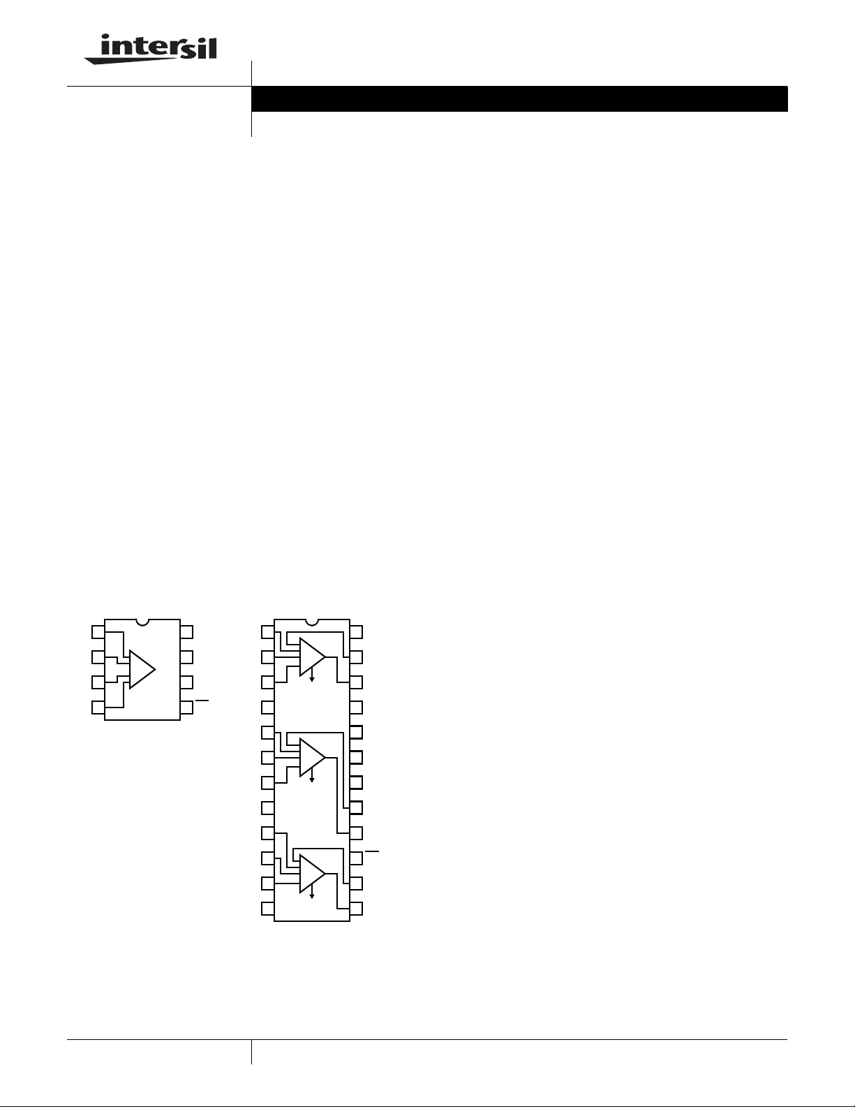
Pinouts
EL5172
(8 LD SOIC, MSOP)
TOP VIEW
EL5372
(24 LD QSOP)
TOP VIEW
FN7311.8
Features
• Differential input range ±2.3V
• 250MHz 3dB bandwidth
• 800V/µs slew rate
• 60mA maximum output current
• Single 5V or dual ±5V supplies
• Low power - 5mA to 6mA per channel
• Pb-free available (RoHS compliant)
Applications
• Twisted-pair receivers
• Differential line receivers
• VGA over twisted-pair
• ADSL/HDSL receivers
• Differential to single-ended amplification
• Reception of analog signals in a noisy environment
FB
IN+
IN-
REF
1
2
+
-
3
4
OUT
8
VS-
7
VS+
6
EN
5
REF1
INP1
INN1
NC
REF2
INP2
INN2
NC
REF3
INP3
INN3
NC
1
2
+
-
3
4
5
6
+
-
7
8
9
10
+
11
-
12
24
23
22
21
20
19
18
17
16
15
14
13
NC
FB1
OUT1
NC
VSP
VSN
NC
FB2
OUT2
EN
FB3
OUT3
1
CAUTION: These devices are sensitive to electrostatic discharge; follow proper IC Handling Procedures.
1-888-INTERSIL or 1-888-468-3774
| Intersil (and design) is a registered trademark of Intersil Americas Inc.
Copyright © Intersil Americas Inc. 2002-2005, 2008. All Rights Reserved.
All other trademarks mentioned are the property of their respective owners.
EL5172, EL5372
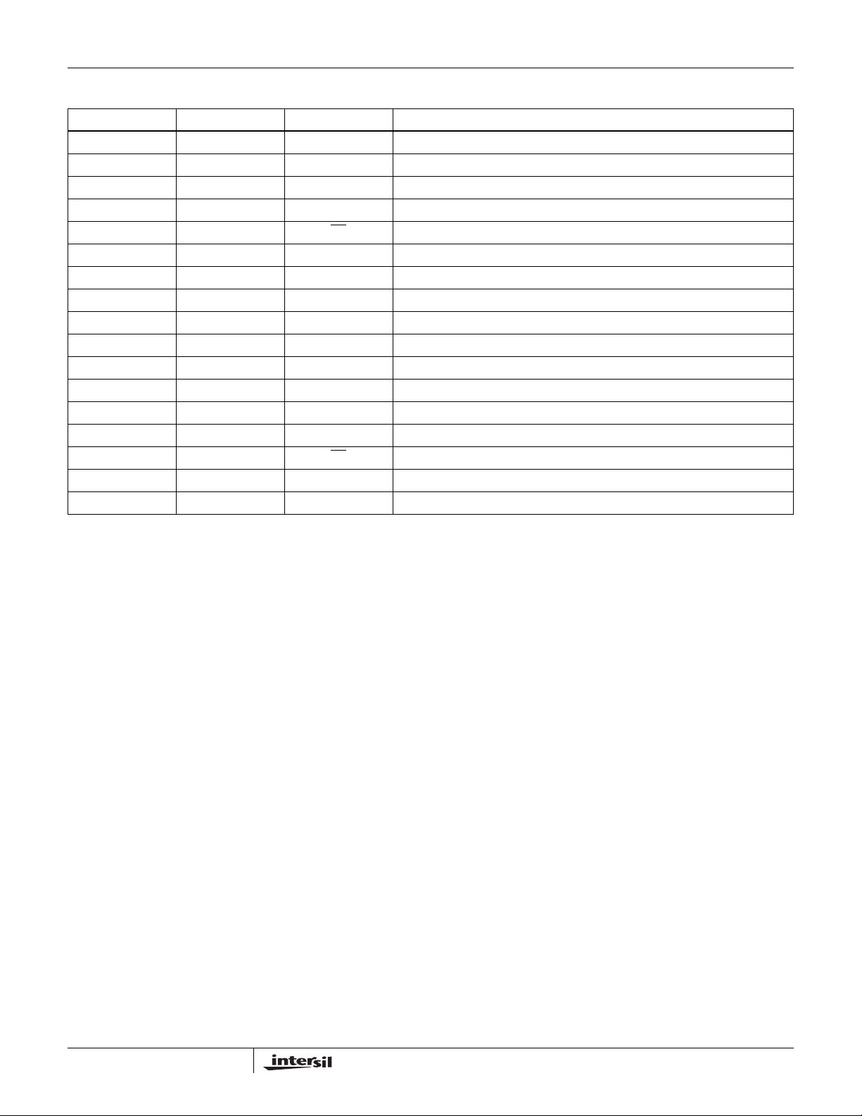
Ordering Information
PART NUMBER PART MARKING PACKAGE PKG. DWG. #
EL5172IS 5172IS 8 Ld SOIC (150 mil) MDP0027
EL5172IS-T7* 5172IS 8 Ld SOIC (150 mil) MDP0027
EL5172IS-T13* 5172IS 8 Ld SOIC (150 mil) MDP0027
EL5172ISZ (Note) 5172ISZ 8 Ld SOIC (150 mil) (Pb-free) MDP0027
EL5172ISZ-T7* (Note) 5172ISZ 8 Ld SOIC (150 mil) (Pb-free) MDP0027
EL5172ISZ-T13* (Note) 5172ISZ 8 Ld SOIC (150 mil) (Pb-free) MDP0027
EL5172IY h 8 Ld MSOP (3.0mm) MDP0043
EL5172IY-T7* h 8 Ld MSOP (3.0mm) MDP0043
EL5172IY-T13* h 8 Ld MSOP (3.0mm) MDP0043
EL5172IYZ (Note) BAAWA 8 Ld MSOP (3.0mm) (Pb-free) MDP0043
EL5172IYZ-T7* (Note) BAAWA 8 Ld MSOP (3.0mm) (Pb-free) MDP0043
EL5172IYZ-T13* (Note) BAAWA 8 Ld MSOP (3.0mm) (Pb-free) MDP0043
EL5372IU EL5372IU 24 Ld QSOP (150 mil) MDP0040
EL5372IU-T7* EL5372IU 24 Ld QSOP (150 mil) MDP0040
EL5372IU-T13* EL5372IU 24 Ld QSOP (150 mil) MDP0040
EL5372IUZ (Note) EL5372IUZ 24 Ld QSOP (150 mil) (Pb-free) MDP0040
EL5372IUZ-T7* (Note) EL5372IUZ 24 Ld QSOP (150 mil) (Pb-free) MDP0040
EL5372IUZ-T13* (Note) EL5372IUZ 24 Ld QSOP (150 mil) (Pb-free) MDP0040
*Please refer to TB347 for details on reel specifications.
NOTE: These Intersil Pb-free plastic packaged products employ special Pb-free material sets; molding compounds/die attach materials and 100%
matte tin plate PLUS ANNEAL - e3 termination finish, which is RoHS compliant and compatible with both SnPb and Pb-free soldering operations.
Intersil Pb-free products are MSL classified at Pb-free peak reflow temperatures that meet or exceed the Pb-free requirements of IPC/JEDEC J
STD-020.
2
FN7311.8
January 25, 2008
EL5172, EL5372
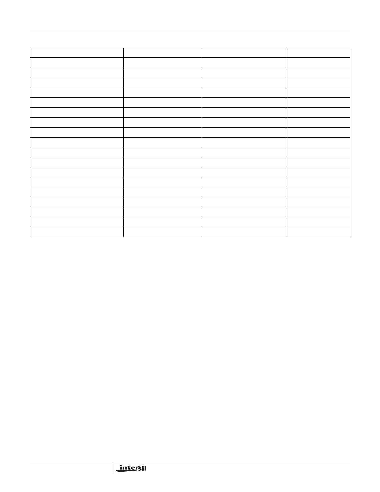
Absolute Maximum Ratings (T
Supply Voltage (VS+ to VS-) . . . . . . . . . . . . . . . . . . . . . . . . . . . .12V
Maximum Output Current. . . . . . . . . . . . . . . . . . . . . . . . . . . . ±60mA
Storage Temperature Range . . . . . . . . . . . . . . . . . .-65°C to +150°C
= +25°C) Thermal Information
A
Operating Junction Temperature . . . . . . . . . . . . . . . . . . . . . . +135°C
Ambient Operating Temperature . . . . . . . . . . . . . . . .-40°C to +85°C
Pb-free reflow profile . . . . . . . . . . . . . . . . . . . . . . . . . .see link below
http://www.intersil.com/pbfree/Pb-FreeReflow.asp
CAUTION: Do not operate at or near the maximum ratings listed for extended periods of time. Exposure to such conditions may adversely impact product reliability and
result in failures not covered by warranty.
IMPORTANT NOTE: All parameters having Min/Max specifications are guaranteed. Typ values are for information purposes only. Unless otherwise noted, all tests are
at the specified temperature and are pulsed tests, therefore: T
Electrical Specifications V
+ = +5V, VS- = -5V, TA = +25°C, VIN = 0V, RL = 500Ω, RF = 0, RG = OPEN, CL = 2.7pF, Unless Otherwise
S
Specified.
= TC = T
J
A
PARAMETER DESCRIPTION CONDITIONS MIN TYP MAX UNIT
AC PERFORMANCE
BW -3dB Bandwidth A
=1, CL = 2.7pF 250 MHz
V
A
=2, RF = 1000Ω, CL = 2.7pF 70 MHz
V
AV =10, RF = 1000Ω, CL = 2.7pF 10 MHz
BW ±0.1dB Bandwidth A
SR Slew Rate V
t
STL
t
OVR
Settling Time to 0.1% V
Output Overdrive Recovery Time 20 ns
=1, CL = 2.7pF 25 MHz
V
V
OUT
OUT
OUT
= 3V
= 3V
= 2V
, 20% to 80%, EL5172 550 800 1000 V/µs
P-P
, 20% to 80%, EL5372 550 700 1000 V/µs
P-P
P-P
10 ns
GBWP Gain Bandwidth Product 100 MHz
V
BW (-3dB) V
REF
V
SR V
REF
V
N
I
N
HD2 Second Harmonic Distortion V
HD3 Third Harmonic Distortion V
dG Differential Gain at 3.58MHz R
dθ Differential Phase at 3.58MHz R
e
S
-3dB Bandwidth AV =1, CL = 2.7pF 120 MHz
REF
Slew Rate V
REF
OUT
= 2V
, 20% to 80% 600 V/µs
P-P
Input Voltage Noise at f = 11kHz 26 nV/√Hz
Input Current Noise at f = 11kHz 2 pA/√Hz
= 1V
OUT
V
= 2V
OUT
= 1V
OUT
V
= 2V
OUT
= 150Ω, AV = 2 0.04 %
L
= 150Ω, AV = 2 0.41 °
L
, 5MHz -66 dBc
P-P
, 50MHz -63 dBc
P-P
, 5MHz -84 dBc
P-P
, 50MHz -76 dBc
P-P
Channel Separation at 100kHz EL5372 only 90 dB
INPUT CHARACTERISTICS
V
OS
I
IN
R
IN
C
IN
Input Referred Offset Voltage ±7 ±25 mV
Input Bias Current (VIN, V
INB
, V
)-14-6-3µA
REF
Differential Input Resistance 300 kΩ
Differential Input Capacitance 1pF
DMIR Differential Input Range ±2.1 ±2.38 ±2.5 V
CMIR+ Common Mode Positive Inpu t Range at V
CMIR- Common Mode Positive Input Range at V
V
REFIN+
V
REFIN-
Reference Input Positive Voltage Range VIN+ = VIN- = 0V 3.3 3.7 V
Reference Input Negative Voltage Range VIN+ = VIN- = 0V -3.9 -3.6
+, VIN-3.33.5V
IN
+, VIN- -4.5 -4.3
IN
3
FN7311.8
January 25, 2008
EL5172, EL5372
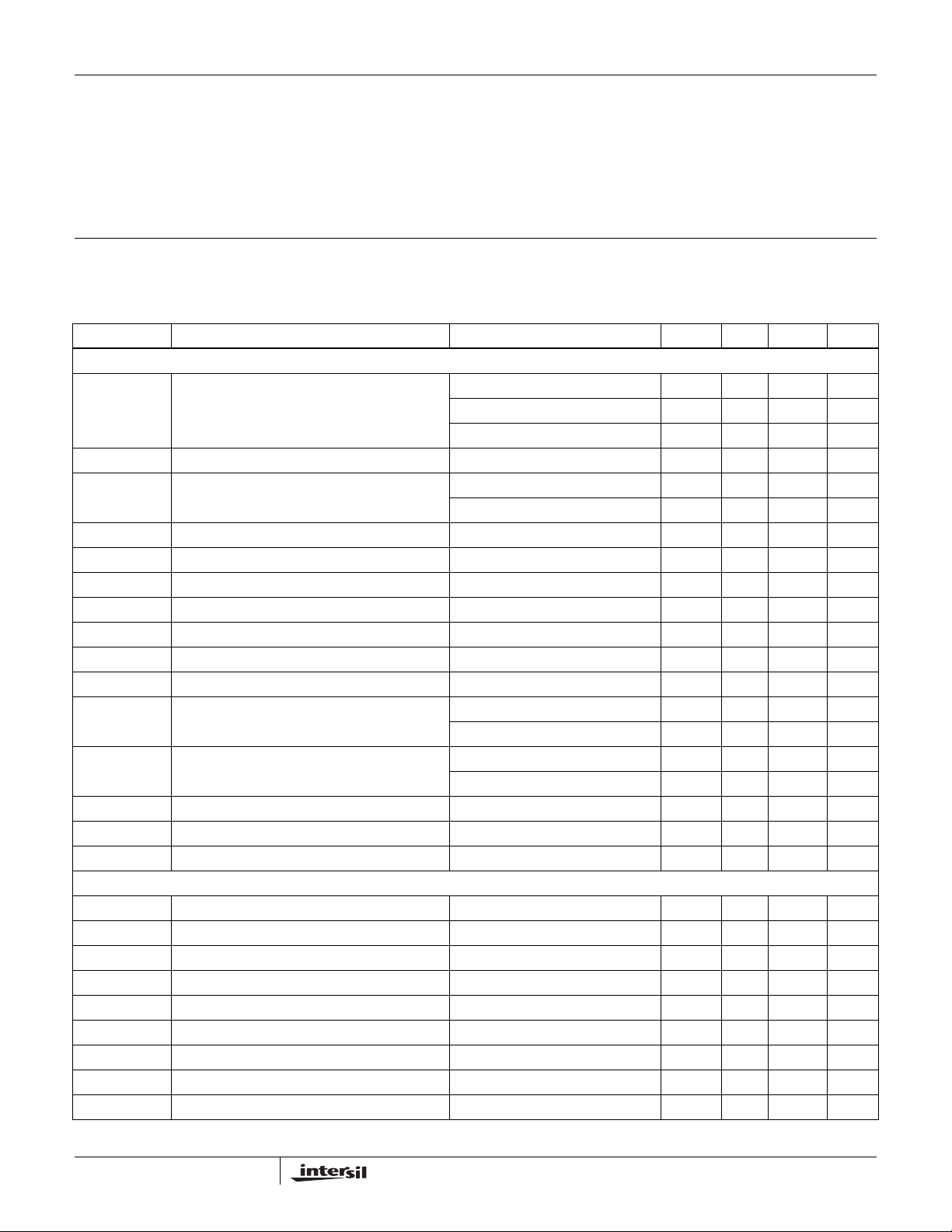
Electrical Specifications V
+ = +5V, VS- = -5V, TA = +25°C, VIN = 0V, RL = 500Ω, RF = 0, RG = OPEN, CL = 2.7pF, Unless Otherwise
S
Specified. (Continued)
PARAMETER DESCRIPTION CONDITIONS MIN TYP MAX UNIT
CMRR Input Common Mode Rejection Ratio V
Gain Gain Accuracy V
= ±2.5V 75 95 dB
IN
= 1 0.985 1 1.015 V
IN
OUTPUT CHARACTERISTICS
V
OUT
Positive Output Voltage Swing RL = 500Ω to GND 3.3 3.63 V
Negative Output Voltage Swing RL = 500Ω to GND -3.87 -3.5 V
I
(Max) Maximum Output Current RL = 10Ω ±60 ±95 mA
OUT
R
OUT
Output Impedance 100 mΩ
SUPPLY
V
SUPPLY
I
S (on)
I
+ Positive Power Supply Current - Disabled EN pin tied to 4.8V, EL5172 80 100 µA
S (off)
I
- Negative Power Supply Current - Disabled -150 -120 -90 µA
S (off)
Supply Operating Range VS+ to VS-4.7511V
Power Supply Current Per Channel - Enabled 4.6 5.6 7 mA
EN
pin tied to 4.8V, EL5372 1.7 5 µA
PSRR Power Supply Rejection Ratio VS from ±4.5V to ±5.5V 50 58 dB
ENABLE
t
EN
t
DS
V
IH
V
IL
I
IH-EN
I
IL-EN
Enable Time 150 ns
Disable Time 1.4 µs
EN Pin Voltage for Power-up VS+ - 1.5 V
EN Pin Voltage for Shut-down VS+ - 0.5 V
EN Pin Input Current High Per Channel At V
EN Pin Input Current Low Per Channel At V
= 5V 40 60 µA
EN
= 0V -10 -3 µA
EN
4
FN7311.8
January 25, 2008
EL5172, EL5372
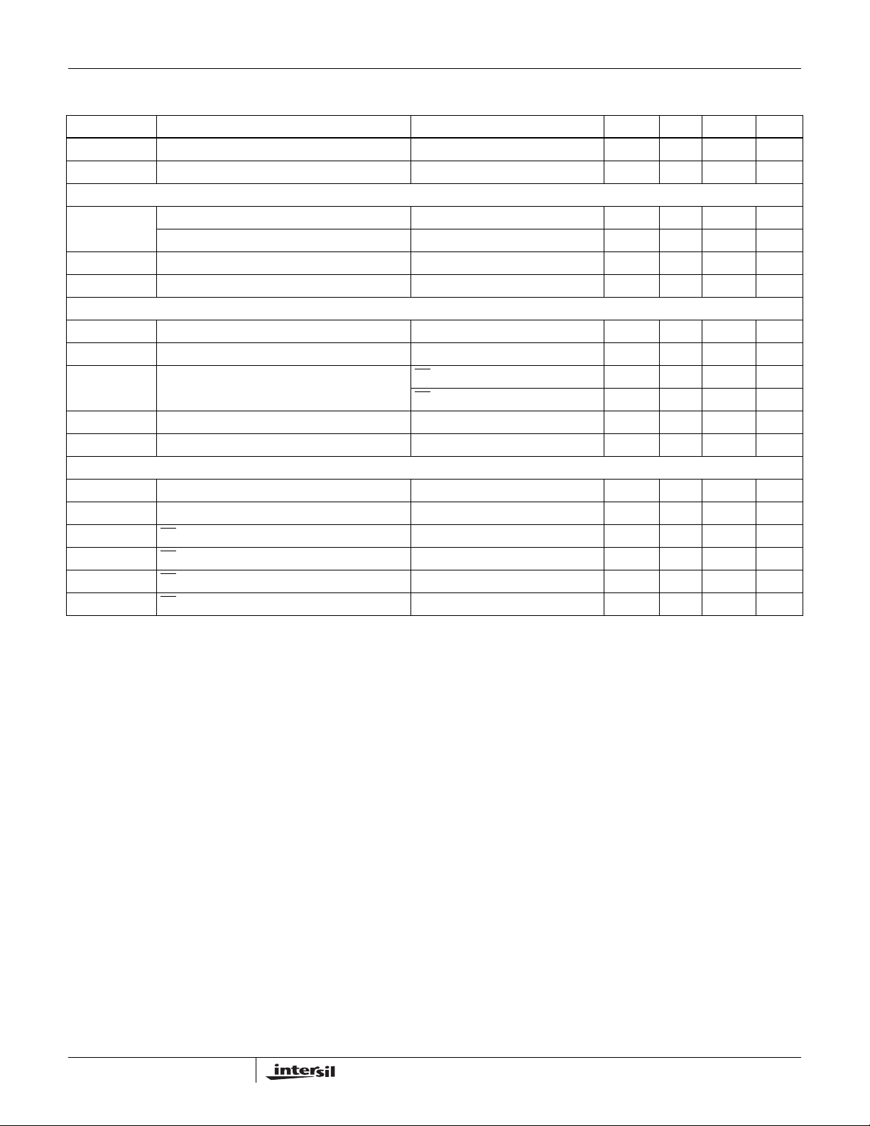
Pin Descriptions
EL5172 EL5372 PIN NAME PIN FUNCTION
1 FB Feedback input
2 IN+ Non-inverting input
3 IN- Inverting input
4 REF Sets the common mode output voltage level
5EN
6 VS+ Positive supply voltage
7 VS- Negative supply voltage
8 OUT Output voltage
1, 5, 9 REF1, 2, 3 Reference input, controls common-mode output voltage
2, 6, 10 INP1, 2, 3 Non-inverting inputs
3, 7, 11 INN1, 2, 3 Inverting inputs
4, 8, 12, 18, 21, 24 NC No connect; grounded for best crosstalk performance
13, 16, 22 OUT1, 2, 3 Non-inverting outputs
14, 17, 23 FB1, 2, 3 Feedback from outputs
15 EN
19 VSN Negative supply
20 VSP Positive supply
Enabled when this pin is floating or the applied voltage ≤ VS+ - 1.5
Enabled when this pin is floating or the applied voltage ≤ VS+ - 1.5
5
FN7311.8
January 25, 2008
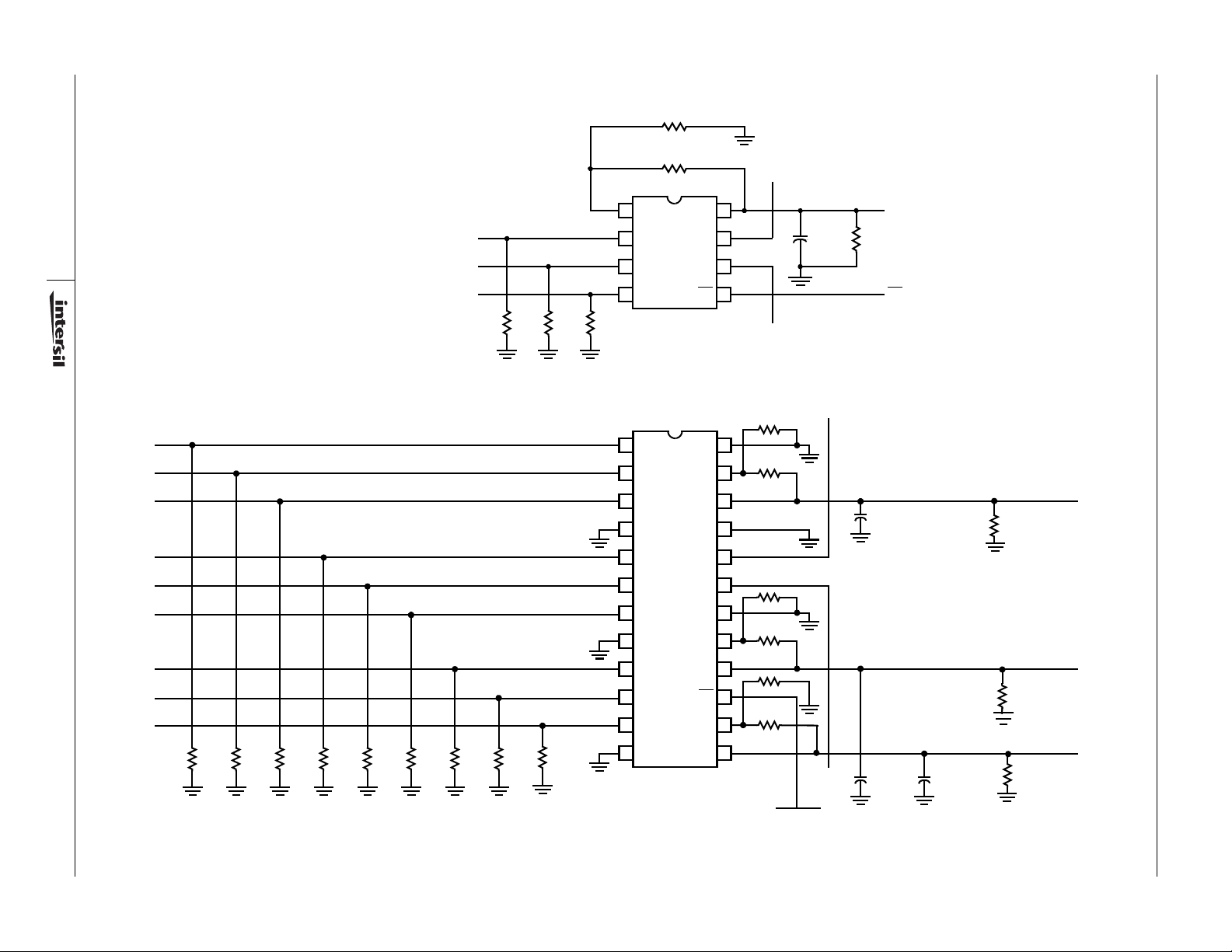
Connection Diagrams
R
G
RF = 0Ω
-5V
FB
1
INP
INP
6
INN
REF
R
S2
50Ω
50Ω
S3
S2
50Ω
R
R
REF1
INP1
INN1
REF2
INP2
INN2
REF3
INP3
INN3
2
INN
3
REF
4
1
REF1
INP1
2
INN1
3
NC
4
REF2
5
INP2
6
INN2
7
NC
8
REF3
9
INP3
10
INN3
11
EL5172
OUT
VSN
VSP
EN
NC
FB1
OUT1
NC
VSP
VSN
NC
FB2
OUT2
EN
FB3
8
C
7
L
2.7pF
R
L
500Ω
VOUT
6
5
EN
+5V
R
G
24
R
F
+5V
EL5172, EL5372
23
22
21
C
L1
2.7pF
R
L1
500Ω
OUT1
20
19
R
G
18
R
F
17
16
R
R
G
15
R
14
F
L2
500Ω
OUT2
R
SP1
50Ω
50Ω
January 25, 2008
SN1
SR1
50Ω
50Ω
SP2
SN2
50Ω
50Ω
SR2
50Ω
SP3
50Ω
SN3
SR3
50Ω
NC
12
EL5372
OUT3
13
-5V
C
L2
2.7pF
C
L3
2.7pF
R
L3
500Ω
OUT3
R
R
R
R
R
R
R
R
ENABLE
FN7311.8

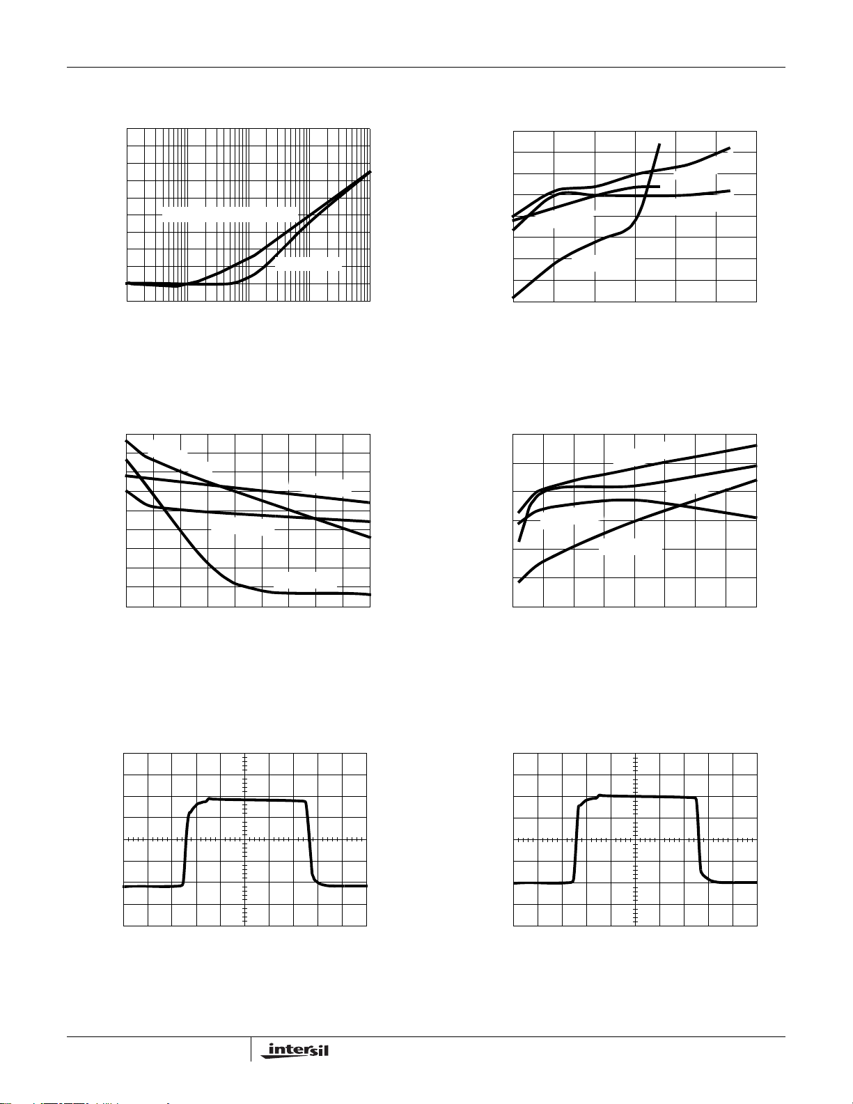
Typical Performance Curves
EL5172, EL5372
= 1, RL = 500Ω, CL = 2.7pF
A
V
4
3
2
1
0
-1
-2
-3
MAGNITUDE (dB)
-4
-5
-6
1M
VS = ±5V
VS = ±2.5V
10M 100M 1G
FREQUENCY (Hz)
AV = 1, RL = 100Ω, CL = 2.7pF
4
3
2
1
0
-1
-2
-3
MAGNITUDE (dB)
-4
-5
-6
1M
10M 100M 1G
VS = ±5V
VS = ±2.5V
FREQUENCY (Hz)
FIGURE 1. FREQUENCY RESPONSE vs SUPPLY VOLTAGE FIGURE 2. FREQUENCY RESPONSE vs SUPPLY VOLTAGE
= ±5V, RL = 500Ω, CL = 2.7pF
V
S
4
3
2
1
0
AV = 1
AV = 2
NORMALIZED GAIN (dB)
-1
-2
-3
-4
-5
-6
1M
AV = 10
10M 100M 1G
AV = 5
FREQUENCY (Hz)
FIGURE 3. FREQUENCY RESPONSE vs VARIOUS GAIN FIGURE 4. FREQUENCY RESPONSE vs C
VS = ±5V, AV = 1, RL = 500Ω
5
4
3
2
1
0
-1
-2
MAGNITUDE (dB)
-3
-4
-5
1M
CL = 56pF
CL = 33pF
CL = 15pF
CL = 10pF
CL = 2.7pF
10M 100M 1G
FREQUENCY (Hz)
L
V
= ±5V, AV = 1, RL = 500Ω
S
5
4
3
2
1
0
-1
-2
MAGNITUDE (dB)
-3
-4
-5
1M
CL = 10pF
CL = 2.7pF
10M 100M 1G
FREQUENCY (Hz)
FIGURE 5. FREQUENCY RESPONSE vs C
7
CL = 56pF
CL = 33pF
CL = 15pF
V
= ±5V, AV = 2, RL = 500Ω, CL = 2.7pF
S
4
3
2
1
0
-1
-2
-3
-4
NORMALIZED GAIN (dB)
-5
-6
1M
L
FIGURE 6. FREQUENCY RESPONSE FOR VARIOUS R
10M 100M 1G
FREQUENCY (Hz)
RF = 1kΩ
RF = 500Ω
RF = 200Ω
F
FN7311.8
January 25, 2008

Typical Performance Curves (Continued)
= 1, RL = 500Ω, CL = 2.7pF
A
V
4
3
2
1
0
-1
NORMINALIZED GAIN (dB)
-2
-3
-4
-5
-6
1M
VS = ±2.5V
10M 100M 1G
FREQUENCY (Hz)
FIGURE 7. FREQUENCY RESPONSE FOR V
VS = ±5V
REF
EL5172, EL5372
GAIN (dB)
60
50
40
30
20
10
-10
-20
-30
-40
0
10k
100k 10M 500M
1M
FREQUENCY (Hz)
100M
FIGURE 8. OPEN LOOP GAIN
270
225
180
135
90
45
0
-45
-90
-135
-180
PHASE (°)
100
10
1
IMPEDENCE (Ω)
0.1
10k
100k 1M 100M
FREQUENCY (Hz)
10M
-10
-20
-30
-40
-50
PSRR (dB)
-60
-70
-80
-90
0
PSRR+
PSRR-
1k
10k 1M 100M
100k
FREQUENCY (Hz)
10M
FIGURE 9. OUTPUT IMPEDANCE vs FREQUENCY FIGURE 10. PSRR vs FREQUENCY
100
90
80
70
60
50
40
CMRR (dB)
30
20
10
0
100k
1M 100M
10M
FREQUENCY (Hz)
1G
VOLTAGE NOISE (nV/√Hz)
CURRENT NOISE (pA/√Hz)
100
1k
E
N
10
I
N
1
100 100k 10M
10
10k
1k
FREQUENCY (Hz)
1M
FIGURE 11. CMRR vs FREQUENCY FIGURE 12. VOLTAGE AND CURRENT NOISE vs FREQUENCY
8
FN7311.8
January 25, 2008
EL5172, EL5372
Typical Performance Curves (Continued)
V
= ±5V, RL = 500Ω, f = 5MHz
0
-10
-20
-30
-40
CH1 <=> CH2, CH2 <=> CH3
CH1 <=> CH3
1M 100M
10M
FREQUENCY (Hz)
1G
GAIN (dB)
-50
-60
-70
-80
-90
-100
100k
FIGURE 13. CHANNEL ISOLATION vs FREQUENCY FIGURE 14. HARMONIC DISTORTION vs OUTPUT VOLTAGE
S
-45
-50
-55
-60
-65
-70
DISTORTION (dB)
-75
-80
-85
1
A
(
2
D
H
A
(
3
D
)
1
=
A
V
(
2
HD
HD3 (AV = 1)
4
3
25
V
OP-P
H
(V)
)
2
=
V
)
2
=
V
7
6
VS = ±5V, f = 5MHz, V
= 2V @AV = 2
V
OP-P
-45
-50
-55
-60
-65
-70
-75
DISTORTION (dB)
-80
-85
-80
H
D
3
(
A
V
=
2
)
200 700
100 600 900400 1000
300 500 800
H
OP-P
D
2
R
LOAD
= 1V @AV = 1,
(
A
=
1
)
V
HD3 (AV = 1)
(Ω)
VS = ±5V, RL = 500Ω, V
= 2V for AV = 2
V
OP-P
-40
-50
H
D
2
(
A
=
2
V
)
-60
)
1
=
A
(
V
2
D
-70
-80
DISTORTION (dB)
-90
-100
H
525
03515 40
10 20 30
FREQUENCY (MHz)
= 1V FOR AV = 1,
OP-P
A
(
V
2
D
H
HD3 (AV = 1)
)
2
=
)
2
=
A
(
V
3
D
H
FIGURE 15. HARMONIC DISTORTION vs LOAD RESISTANCE FIGURE 16. HARMONIC DISTORTION vs FREQUENCY
50mV/DIV
10ns/DIV
0.5V/DIV
10ns/DIV
FIGURE 17. SMALL SIGNAL TRANSIENT RESPONSE FIGURE 18. LARGE SIGNAL TRANSIENT RESPONSE
9
FN7311.8
January 25, 2008

Typical Performance Curves (Continued)
M = 100ns, CH1 = 200mV/DIV, CH2 = 5V/DIV
EL5172, EL5372
M = 400ns, CH1 = 200mV/DIV, CH2 = 5V/DIV
CH1
CH2
100ns/DIV
CH1
CH2
400ns/DIV
FIGURE 19. ENABLED RESPONSE FIGURE 20. DISABLED RESPONSE
JEDEC JESD51-3 LOW EFFECTIVE THERMAL
CONDUCTIVITY TEST BOARD
1.2
1.0
870mW
0.8
625mW
0.6
0.4
486mW
0.2
POWER DISSIPATION (W)
0
0 255075100 150
MSOP8
θ
= +206°C/W
JA
AMBIENT TEMPERATURE (°C)
QSOP24
θ
= +115°C/W
JA
SOIC8
θ
= +160°C/W
JA
12585
JEDEC JESD51-7 HIGH EFFECTIVE THERMAL
CONDUCTIVITY TEST BOARD
1.4
1.136W
1.2
1.0
909mW
0.8
870mW
0.6
MSOP8/10
θ
= +115°C/W
JA
0 255075100 150
AMBIENT TEMPERATURE (°C)
POWER DISSIPATION (W)
0.4
0.2
0
QSOP24
θ
JA
= +88°C/W
SOIC8
θ
= +110°C/W
JA
12585
FIGURE 21. PACKAGE POWER DISSIP A TION vs AMBIENT
TEMPERATURE
Simplified Schematic
VS+
I
I
2
1
R
D1
FBP
Q
2
3
10
VIN+
Q
VIN-
1
Q
FIGURE 22. PACKAGE POWER DISSIP A TION vs AMBIENT
TEMPERATURE
R
I
I
4
3
R
D2
FBN
Q
R
4
R
4
3
Q
8
Q
7
25
R
2
1
VS-
V
B1
Q
9
x1 V
Q
6
V
B2
C
C
OUT
FN7311.8
January 25, 2008

EL5172, EL5372
Description of Operation and Application
Information
Product Description
The EL5172 and EL5372 are wide bandwidth, low power
and single/differential ended to single ended output
amplifiers. The EL5172 is a single channel differential to
single ended amplifier. The EL5372 is a triple channel
differential to single ended amplifier. The EL5172 and
EL5372 are internally compensated for closed loop gain of
+1 or greater. Connected in gain of 1 and driving a 500Ω
load, the EL5172 and EL5372 have a -3dB bandwidth of
250MHz. Driving a 150Ω load at gain of 2, the bandwidth is
about 50MHz. The bandwidth at the REF input is about
450MHz. The EL5172 and EL5372 are available with a
power-down feature to reduce the power while the amplifier
is disabled.
Input, Output and Supply Voltage Range
The EL5172 and EL5372 have been designed to operate
with a single supply voltage of 5V to 10V or a split supplies
with its total voltage from 5V to 10V. The amplifiers have an
input common mode voltage range from -4.3V to 3.3V for
±5V supply. The differential mode input range (DMIR)
between the two inputs is about from -2.3V to +2.3V. The
input voltage range at the REF pin is from -3.6V to 3.3V. If
the input common mode or differential mode signal is outside
the above-specified ranges, it will cause the output signal to
be distorted.
The output of the EL5172 and EL5372 can swing from -3.8V
to 3.6V at 500Ω load at ±5V supply. As the load resistance
becomes lower, the output swing is reduced respectively.
Over All Gain Settings
The gain setting for the EL5172 and the EL5372 is similar to
the conventional operational amplifier. The output voltage is
equal to the difference of the inputs plus V
times the gain.
R
⎛⎞
F
V
V(IN+VIN-V
O
+ ) 1
REF
--------
+
×–=
⎜⎟
R
⎝⎠
G
and then
REF
Choice of Feedback Resistor and Gain Bandwidth
Product
For applications that require a gain of +1, no feedback
resistor is required. Just short the OUT pin to the FB pin. For
gains greater than +1, the feedback resistor forms a pole
with the parasitic capacitance at the inverting input. As this
pole becomes smaller, the amplifier's phase margin is
reduced. This causes ringing in the time domain and
peaking in the frequency domain. Therefore, R
has some
F
maximum value that should not be exceeded for optimum
performance. If a large value of R
capacitor in the few Pico farad range in parallel with R
must be used, a small
F
can
F
help to reduce the ringing and peaking at the expense of
reducing the bandwidth.
The bandwidth of the EL5172 and EL5372 depends on the
load and the feedback network. R
and RG appear in
F
parallel with the load for gains other than +1. As this
combination gets smaller, the bandwidth falls off.
Consequently, R
also has a minimum value that should not
F
be exceeded for optimum bandwidth performance. For a
gain of +1, R
optimum response is obtained with R
1kΩ. For A
= 0 is optimum. For the gains other than +1,
F
= 2 and RF = RG = 1kΩ, the BW is about 80MHz
V
between 500Ω to
F
and the frequency response is very flat.
The EL5172 and EL5372 have a gain bandwidth product of
100MHz. For gains ≥5, its bandwidth can be predicted by
Equation 1:
Gain BW 100MHz=×
(EQ. 1)
Driving Capacitive Loads and Cables
The EL5172 and EL5372 can drive 56pF capacitance in
parallel with 500Ω load to ground with 4dB of peaking at gain
of +1. If less peaking is desired in applications, a small
series resistor (usually between 5Ω to 50Ω) can be placed in
series with each output to eliminate most peaking. However,
this will reduce the gain slightly. If the gain setting is greater
than 1, the gain resistor R
for any gain loss which may be created by the additional
series resistor at the output.
can then be chosen to make up
G
VIN+
V
V
IN
REF
FB
R
EN
+
-
Σ G/B V
+
-
O
When used as a cable driver, double termination is always
recommended for reflection-free performance. For those
applications, a back-termination series resistor at the
amplifier's output will isolate the amplifier from the cable and
allow extensive capacitive drive. However, other applications
may have high capacitive loads without a back-termination
resistor. Again, a small series resistor at the output can help
to reduce peaking.
R
F
G
Disable/Power-Down
The EL5172 and EL5372 can be disabled and its outputs
placed in a high impedance state. The turn-off time is about
1.4µs and the turn-on time is about 150ns. When disabled,
FIGURE 23.
11
the amplifier's supply current is reduced to 80µA for I
January 25, 2008
+ and
S
FN7311.8

EL5172, EL5372
120µA for IS- typically, thereby effectively eliminating the
power consumption. The amplifier's power-down can be
controlled by standard CMOS signal levels at the ENABLE
pin. The applied logic signal is relative to V
EN
pin float or applying a signal that is less than 1.5V below
V
+ will enable the amplifier. The amplifier will be disabled
S
when the signal at EN
pin is above VS+ - 0.5V. If a TTL
+ pin. Letting the
S
signal is used to control the enabled/disabled function,
Figure 24 could be used to convert the TTL signal to CMOS
signal.
5V
10k
CMOS/TTL
1k
FIGURE 24.
EN
Output Drive Capability
The EL5172 and EL5372 have internal short circuit
protection. Its typical short circuit current is ±95mA. If the
output is shorted indefinitely, the power dissipation could
easily increase such that the part will be destroyed.
Maximum reliability is maintained if the output current never
exceeds ±60mA. This limit is set by the design of the internal
metal interconnections.
Power Dissipation
With the high output drive capability of the EL5172 and
EL5372, it is possible to exceed the +135°C absolute
maximum junction temperature under certain load current
conditions. Therefore, it is important to calculate the
maximum junction temperature for the application to
determine if the load conditions or package types need to be
modified for the amplifier to remain in the safe operating
area.
The maximum power dissipation allowed in a package is
determined according to Equation 2:
T
–
JMAXTAMAX
PD
•T
•T
• θ
Assuming the REF pin is tied to GND for V
-------------------------------------------- -
=
MAX
JMAX
AMAX
= Thermal resistance of the package
JA
Θ
JA
= Maximum junction temperature
= Maximum ambient temperature
= ±5V
S
application, the maximum power dissipation actually
produced by an IC is the total quiescent supply current times
the total power supply voltage, plus the power in the IC due
to the load, or:
(EQ. 2)
For sourcing, use Equation 3:
PD
MAX
VSI
SMAXVS
+( V
OUT
)
OUT
------------------- -
R
LOAD
i××–+×=
(EQ. 3)
V
For sinking, use Equation 4:
PD
MAX
VSI
SMAXVOUT
( VS-) I
LOAD
] i××–+×[=
(EQ. 4)
Where:
•V
= Total supply voltage
S
•I
•V
•R
•I
= Maximum quiescent supply current per channel
SMAX
= Maximum output voltage of the application
OUT
= Load resistance
LOAD
= Load current
LOAD
• i = Number of channels
By setting the two PD
can solve the output current and R
equations equal to each other, we
MAX
to avoid the device
LOAD
overheat.
Power Supply Bypassing and Printed Circuit
Board Layout
As with any high frequency device, a good printed circuit
board layout is necessary for optimum performance. Lead
lengths should be as short as possible. The power supply
pin must be well bypassed to reduce the risk of oscillation.
For normal single supply operation, where the V
connected to the ground plane, a single 4.7µF tantalum
capacitor in parallel with a 0.1µF ceramic capacitor from V
to GND will suffice. This same capacitor combination should
be placed at each supply pin to ground if split supplies are to
be used. In this case, the V
- pin becomes the negative
S
supply rail.
For good AC performance, parasitic capacitance should be
kept to a minimum. Use of wire wound resistors should be
avoided because of their additional series inductance. Use
of sockets should also be avoided if possible. Sockets add
parasitic inductance and capacitance that can result in
compromised performance. Minimizing parasitic capacitance
at the amplifier's inverting input pin is very important. The
feedback resistor should be placed very close to the
inverting input pin. Strip line design techniques are
recommended for the signal traces.
- pin is
S
S
+
12
FN7311.8
January 25, 2008

Typical Applications
EL5172, EL5372
0Ω
50
EL5173,
EL5373
OR
EL5172,
EL5372
50
= 100Ω
Z
O
FIGURE 25. TWISTED PAIR CABLE RECEIVER
As the signal is transmitted through a cable, the high
frequency signal will be attenuated. One way to compensate
for this loss is to boost the high frequency gain at the
receiver side.
V
V
V
V
FB
IN
INB
REF
R
2
EL5172,
EL5372
ZO = 100Ω
C
50Ω
50Ω
R
1
1
R
3
V
OUT
50Ω
50Ω
V
FB
V
IN
V
INB
V
REF
GAIN
(dB)
1 + R2/(R1 + R3)
EL5172,
EL5372
f
A
V
OUT
1 + R
2/R1
f
C
f
FIGURE 26. COMPENSATED LINE RECEIVER
Level Shifter and Signal Summer
The EL5172 and EL5372 contains two pairs of differential
pair input stages, which make sure that the inputs are all
high impedance inputs. To take advantage of the two high
impedance inputs, the EL5172 and EL5372 can be used as
a signal summer to add two signals together. One signal can
be applied to VIN+, the second signal can be applied to REF
and V
V
Also, the EL5172 and EL5372 can be used as a level shifter
by applying a level control signal to the REF input.
- is ground. The output is equal to Equation 5:
IN
O
VIN( +V
REF
) Gain×+=
(EQ. 5)
13
FN7311.8
January 25, 2008

Small Outline Package Family (SO)
A
D
NN
(N/2)+1
EL5172, EL5372
h X 45¬
PIN #1
E
C
SEATING
PLANE
0.004 C
E1
B
0.010 BM CA
I.D. MARK
1
e
0.010 BM CA
(N/2)
c
SEE DETAIL ‚Ä ö
L1
H
A2
GAUGE
PLANE
A1
b
DETAIL X
L
4¬¨Ðó
MDP0027
SMALL OUTLINE PACKAGE FAMILY (SO)
INCHES
SO16
SYMBOL
(0.150”)
A 0.068 0.068 0.068 0.104 0.104 0.104 0.104 MAX -
A1 0.006 0.006 0.006 0.007 0.007 0.007 0.007 ±0.003 A2 0.057 0.057 0.057 0.092 0.092 0.092 0.092 ±0.002 -
b 0.017 0.017 0.017 0.017 0.017 0.017 0.017 ±0.003 -
c 0.009 0.009 0.009 0.011 0.011 0.011 0.011 ±0.001 D 0.193 0.341 0.390 0.406 0.504 0.606 0.704 ±0.004 1, 3
E 0.236 0.236 0.236 0.406 0.406 0.406 0.406 ±0.008 -
E1 0.154 0.154 0.154 0.295 0.295 0.295 0.295 ±0.004 2, 3
e 0.050 0.050 0.050 0.050 0.050 0.050 0.050 Basic -
L 0.025 0.025 0.025 0.030 0.030 0.030 0.030 ±0.009 -
L1 0.041 0.041 0.041 0.056 0.056 0.056 0.056 Basic -
h 0.013 0.013 0.013 0.020 0.020 0.020 0.020 Reference -
N 8 14 16 16 20 24 28 Reference -
NOTES:
1. Plastic or metal protrusions of 0.006” maximum per side are not included.
2. Plastic interlead protrusions of 0.010” maximum per side are not included.
3. Dimensions “D” and “E1” are measured at Datum Plane “H”.
4. Dimensioning and tolerancing per ASME Y14.5M-1994
SO16 (0.300”)
(SOL-16)
SO20
(SOL-20)
SO24
(SOL-24)
SO28
(SOL-28)
TOLERANCE NOTESSO-8 SO-14
A
0.010
Rev. M 2/07
14
FN7311.8
January 25, 2008

EL5172, EL5372
Quarter Size Outline Plastic Packages Family (QSOP)
E E1
0.010 C A B
C
SEATING
PLANE
0.004 C
A
N
1
B
L1
c
SEE DETAI L "X"
D
PIN #1
I.D. MARK
e
0.007 C A B
(N/2)+1
A
(N/2)
MDP0040
QUARTER SIZE OUTLINE PLASTIC PACKAGES FAMILY
INCHES
SYMBOL
A 0.068 0.068 0.068 Max. A1 0.006 0.006 0.006 ±0.002 A2 0.056 0.056 0.056 ±0.004 -
b 0.010 0.010 0.010 ±0.002 -
c 0.008 0.008 0.008 ±0.001 D 0.193 0.341 0.390 ±0.004 1, 3
E 0.236 0.236 0.236 ±0.008 -
H
E1 0.154 0.154 0.154 ±0.004 2, 3
e 0.025 0.025 0.025 Basic -
L 0.025 0.025 0.025 ±0.009 -
b
L1 0.041 0.041 0.041 Basic -
N 16 24 28 Reference -
NOTES:
1. Plastic or metal protrusions of 0.006” maximum per side are not
included.
2. Plastic interlead protrusions of 0.010” maximum per side are not
included.
3. Dimensions “D” and “E1” are measured at Datum Plane “H”.
4. Dimensioning and tolerancing per ASME Y14.5M-1994.
TOLERANCE NOTESQSOP16 QSOP24 QSOP28
Rev. F 2/07
A2
A1
DETAIL X
GAUGE
PLANE
L
0.010
4¬¨Ðó
15
FN7311.8
January 25, 2008
Mini SO Package Family (MSOP)
M
C
SEATING
PLANE
0.10 C
N LEADS
c
0.25 C A B
E1E
B
e
L1
SEE DETAIL "X"
D
N
1
b
A
(N/2)+1
PIN #1
I.D.
(N/2)
H
M
0.08 C A B
A
EL5172, EL5372
MDP0043
MINI SO PACKAGE FAMILY
SYMBOL
A1.101.10 Max. A1 0.10 0.10 ±0.05 A2 0.86 0.86 ±0.09 -
b 0.33 0.23 +0.07/-0.08 -
c0.180.18 ±0.05 -
D 3.00 3.00 ±0.10 1, 3
E4.904.90 ±0.15 E1 3.00 3.00 ±0.10 2, 3
e0.650.50 Basic -
L0.550.55 ±0.15 -
L1 0.95 0.95 Basic -
N 8 10 Reference -
NOTES:
1. Plastic or metal protrusions of 0.15mm maximum per side are not
included.
2. Plastic interlead protrusions of 0.25mm maximum per side are
not included.
3. Dimensions “D” and “E1” are measured at Datum Plane “H”.
4. Dimensioning and tolerancing per ASME Y14.5M-1994.
MILLIMETERS
TOLERANCE NOTESMSOP8 MSOP10
Rev. D 2/07
A2
GAUGE
A1
L
DETAIL X
PLANE
3¬¨Ðó
0.25
All Intersil U.S. products are manufactured, assembled and tested utilizing ISO9000 quality systems.
Intersil Corporation’s quality certifications can be viewed at www.intersil.com/design/quality
Intersil products are sold by description only. Intersil Corporation reserves the right to make changes in circuit design, software and/or specifications at any time without
notice. Accordingly, the reader is cautioned to verify that data sheets are current before placing orders. Information furnished by Intersil is believed to be accurate and
reliable. However, no responsibility is assumed by Intersil or its subsidiaries for its use; nor for any infringements of patents or other rights of third parties which may result
from its use. No license is granted by implicat ion or oth erwise u nde r any p a tent or p at ent r ights of Intersil or its subsidiaries.
For information regarding Intersil Corporation and its products, see www.intersil.com
16
FN7311.8
January 25, 2008
 Loading...