

查询EL5285CS供应商
T
C
U
D
h
o
E PR
E
D
c
i
n
r
O
C
A
L
P
E
R
D
l
a
w
w
r
o
p
p
u
S
r
e
t
n
i
.
w
®
O
EC
R
O
Data Sheet January 18, 2002
N
t
c
a
t
n
o
c
N
I
-
8
8
8
-
1
ET
L
O
S
B
EN
M
M
O
c
e
T
r
u
o
L
SI
R
E
T
t
s
EM
C
il
T
EN
t
a
r
e
t
n
e
c
s
/t
m
o
.c
EL5285
FN7190
Dual 4ns High-Speed Comparator
The EL5285 comparator is designed
for operation in single supply and dual
supply applications with 5V to 12V
between V
+ and VS-. For single supplies, the inputs can
S
operate from 0.1V below ground for use in ground sensing
applications.
The output side of the comparators can be supplied from a
single supply of 2.7V to 5V. The rail-to-rail output swing
enables direct connection of the comparator to both CMOS
and TTL logic circuits.
The latch input of the EL5285 can be used to hold the
comparator output value by applying a low logic level to the
pin. The EL5285 features two separate comparators
The EL5285 is available in the 14-pin SO package and is
specified for operation over the full -40°C to +85°C
temperature range. Also available are a single (EL5185),
window comparator (EL5287), and quad versions (EL5485
and EL5486).
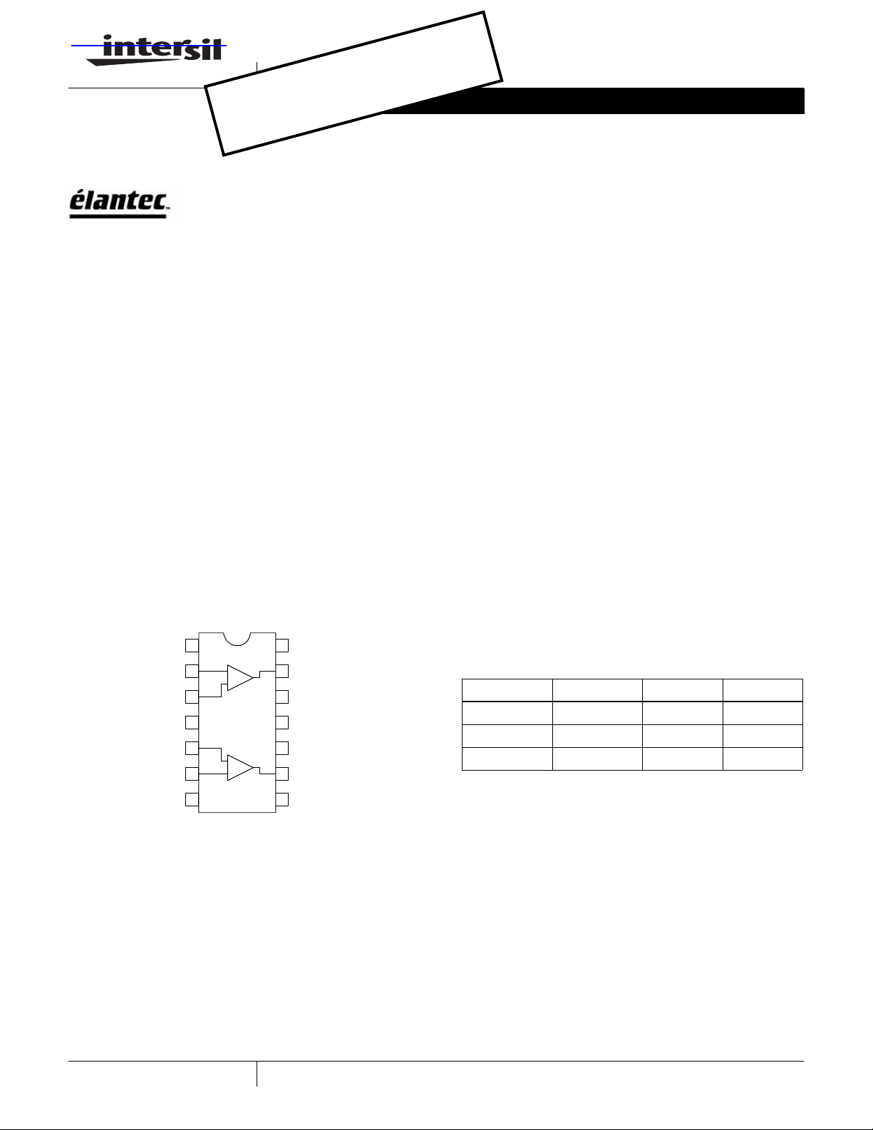
Pinout
EL5285
(14-PIN SO)
TOP VIEW
Features
• 4ns typ. propagation delay
• 5V to 12V input supply
• +2.7V to +5V output supply
• True-to-ground input
• Rail-to-rail outputs
• Active low latch
• Single available (EL5185)
• Window available (EL5287)
• Quad available (EL5485 & EL5486)
• Pin-compatible 8ns family available (EL5x81, EL5283 &
EL5482)
Applications
• Threshold detection
• High speed sampling circuits
• High speed triggers
• Line receivers
• PWM circuits
• High speed V/F converters
VS+
INA+
INA-
NC
INB+
INB-
VS-
1
2
+
-
3
4
5
+
6
-
7
14
13
12
11
10
9
8
VSD
OUTA
LATCHA
NC
LATCHB
OUTB
GND
Ordering Information
PART NUMBER PACKAGE TAPE & REEL PKG. NO.
EL5285CS 14-Pin SO - MDP0027
EL5285CS-T7 14-Pin SO 7” MDP0027
EL5285CS-T13 14-Pin SO 13” MDP0027
1
Copyright © Intersil Americas Inc. 2003. All Rights Reserved. Elantec is a registered trademark of Elantec Semiconductor, Inc.
CAUTION: These devices are sensitive to electrostatic discharge; follow proper IC Handling Procedures.
1-888-INTERSIL or 321-724-7143
| Intersil (and design) is a registered trademark of Intersil Americas Inc.
All other trademarks mentioned are the property of their respective owners.
EL5285
Absolute Maximum Ratings (T
Analog Supply Voltage (V
Digital Supply Voltage (V
Differential Input Voltage . . . . . . . . . . .[(V
Common-mode Input Voltage . . . . . . .[(V
Latch Input Voltage . . . . . . . . . . . . . . . . . . . . -0.2V to [(V
CAUTION: Stresses above those listed in “Absolute Maximum Ratings” may cause permanent damage to the device. This is a stress only rating and operation of the
device at these or any other conditions above those indicated in the operational sections of this specification is not implied.
IMPORTANT NOTE: All parameters having Min/Max specifications are guaranteed. Typical values are for information purposes only. Unless otherwise noted, all tests
are at the specified temperature and are pulsed tests , therefore: T
+ to VS-) . . . . . . . . . . . . . . . . . . . +12.6V
S
to GND). . . . . . . . . . . . . . . . . . . . . .+7V
SD
Electrical Specifications V
= 25°C)
A
Storage Temperature Range . . . . . . . . . . . . . . . . . .-65°C to +150°C
Ambient Operating Temperature . . . . . . . . . . . . . . . .-40°C to +85°C
-) -0.2V] to [(VS+) +0.2V]
S
-) -0.2V] to [(VS+) +0.2V]
S
= ±5V, VSD = 5V, RL = 2.3kΩ, TA = 25°C, unless otherwise specified.
S
+0.2V]
SD)
= TC = T
J
A
Operating Junction Temperature . . . . . . . . . . . . . . . . . . . . . . .125°C
Power Dissipation . . . . . . . . . . . . . . . . . . . . . . . . . . . . . See Curves
PARAMETER DESCRIPTION CONDITION MIN TYP MAX UNIT
INPUT
V
OS
I
B
C
IN
I
OS
V
CM
CMRR Common-mode Rejection Ratio -5.1V < V
Input Offset Voltage V
= 0V, VO = 2.5V 1 4 mV
CM
Input Bias Current -10 -5 µA
Input Capacitance 5pF
Input Offset Current V
= 0V, VO = 2.5V -2.5 0.5 2.5 µA
CM
Input Voltage Range (VS-) - 0.1 (VS+) - 2.25 V
< +2.75V 65 90 dB
CM
OUTPUT
V
OH
V
OL
Output High Voltage V
Output Low Voltage V
> 250mV VSD - 0.6 VSD - 0.4 V
IN
> 250mV GND + 0.25 GND + 0.5 V
IN
DYNAMIC PERFORMANCE
t
+ Positive Going Delay Time VIN = 1V
pd
tpd- Negative Going Delay Time VIN = 1V
, VOD = 50mV 4 6 ns
P-P
, VOD = 50mV 4 6 ns
P-P
SUPPLY
I
+ Positive Analog Supply Current Per comparator 12 13.5 mA
S
IS- Negative Analog Supply Current Per comparator 7.5 8.5 mA
I
SD
Digital Supply Current at No Load Per comparator, output high 5.5 6.5 mA
Per comparator, output low 0.9 1.2 mA
PSRR Power Supply Rejection Ratio 55 80 dB
LATCH
V
LH
V
LL
I
LH
I
LL
+ Latch Disable to High Delay 6 ns
t
d
t
- Latch Disable to Low Delay 6 ns
d
t
s
t
h
t
(D) Minimum Latch Disable Pulse
pw
Latch Input Voltage High 2.0 V
Latch Input Voltage Low 0.8 V
Latch Input Current High V
Latch Input Current Low V
= 3.0V -30 -18 µA
LH
= 0.3V -30 -24 µA
LL
Minimum Setup Time 2 ns
Minimum Hold Time 1ns
10 ns
Width
2
Typical Performance Curves
EL5285
Supply Current vs Supply Voltage
14
VIN=-50mV
RL=2.3kΩ
12
10
8
(mA)
S
6
I
4
2
0
0123456
Offset Voltage vs Temperature
2.5
2
1.5
1
(mV)
OS
V
0.5
0
-0.5
-50 -30 10 30 50 70 90
IS+
IS-
±VS (V)
-10
Temperature (°C)
Output High Voltage vs Temperature
5
4.8
4.6
(V)
OH
V
4.4
4.2
4
-50 -30 10 30 50 70 90
Input Bias Current vs Temperature
9
8
7
6
5
IB (µA)
4
3
2
1
-50 -30 30 50 90
-10
Temperature (°C)
-10 10 70
Temperature (°C)
Output Low Voltage vs Temperature
0.4
0.3
(V)
OL
V
0.2
0.1
-50 -30 10 30 50 70 90
-10
Temperature (°C)
Supply Current vs Temperature (per comparator)
14
12
10
8
6
4
Supply Current (mA)
2
0
-50 -30 10 30 50 70 90
IS+
IS-
-10
Temperature (°C)
3

Typical Performance Curves (Continued)
EL5285
Propagation Delay vs Overdrive
VIN=1V
4.2
4.1
3.9
3.8
Delay Time (ns)
3.7
3.6
3.5
6.8
6.6
6.4
6.2
5.8
5.6
Delay Time (ns)
5.4
5.2
STEP
4
50 100 200 300 400 500 600
150 250 350 450 550
Propagation Delay vs Overdrive
V
=3V
IN
STEP
6
5
0.2 0.4 0.8 1 1.2 1.6 2
0.6 1.4 1.8
TPD+
TPD-
VOD (mV)
TPD+
TPD-
VOD (V)
VS=±5V
VSD=5V
=2.3kΩ
R
L
VS=±5V
VSD=5V
RL=2.3kΩ
Propagation Delay vs Supply Voltage
4.5
4.4
4.3
4.2
4.1
4
3.9
Delay Time (ns)
3.8
3.7
3.6
3.5
4 4.2 4.8 5.2 5.6 5.8 6
Digital Supply Current vs Switching Frequency
(per comparator)
25
VS=±5V
TA=25°C
RL=2.3kΩ
20
15
(mA)
SD
I
10
5
0
0204050
TPD-
4.6
4.4 5 5.4
±VS (V)
VSD=5V
10
Frequency (MHz)
TPD+
VSD=3V
30
VSD=VS+
VOD=50mV
=2.2kΩ
R
L
Propagation Delay vs Overdrive
VIN=5V
7.2
6.8
6.6
6.4
Delay Time (ns)
6.2
5.8
STEP
7
6
0.2 0.4 1 1.4 1.8 2.2 2.6
TPD+
TPD-
0.6 1.2 1.6 2 2.4
0.8
VOD (V)
VS=±5V
VSD=5V
RL=2.3kΩ
Propagation Delay vs Source Resistance
VIN=1V
STEP
16
VS=±5V
VSD=5mV
14
VOD=50mV
RL=2.3kΩ
12
10
8
Delay Time (ns)
6
4
0.4 1 1.40.6
0 0.2 0.8 1.2 1.6 1.8 2
TPD+
TPD-
Source Resistance (kΩ)
4

Typical Performance Curves (Continued)
Propagation Delay vs Load Capacitance
VIN=1V
7.5
6.5
5.5
Delay Time (ns)
4.5
1.4
1.2
0.8
0.6
0.4
Power Dissipation (W)
0.2
STEP
VS=±5V
VSD=5V
7
=50mV
V
OD
R
=2.3kΩ
L
6
5
4
010 40608090100
20 50 7030
Package Power Dissipation vs Ambient Temperature
JEDEC JESD51-7 High Effective Thermal Conductivity Test
Board
1.136W
1
0
0 125755025
TPD+
TPD-
C
(pF)
LOAD
S
O
1
8
4
8
°
C
/
W
Ambient Temperature (°C)
EL5285
15010085
Package Power Dissipation vs Ambient Temperature
JEDEC JESD51-3 Low Effective Thermal Conductivity
Test Board
0.9
0.8
0.7
0.6
0.5
0.4
0.3
Power Dissipation (W)
0.2
0.1
0
0100755025
Output with 50MHz Input
VIN=1V
Output
(5ns/div,
2V/div)
Input
(5ns/div,
0.5V/div)
833mW
P-P
S
O1
1
2
4
0
°
C
/
W
Ambient Temperature (°C)
85
125
Output with 50MHz Input
VIN=3V
Output
(5ns/div,
2V/div)
Input
(5ns/div,
2V/div)
P-P
5

EL5285
Pin Descriptions
PIN NUMBER PIN NAME FUNCTION EQUIVALENT CIRCUIT
1 VS+ Positive supply current
2 INA+ Positive input, channel A
VS+
IN+IN-
3 INA- Negative input, channel A (Reference Circuit 1)
4, 11 NC Not connected
5 INB+ Negative input, channel B (Reference Circuit 1)
6 INB- Positive input, channel B (Reference Circuit 1)
7 VS- Negative supply voltage
8 GND Ground
9 OUTB Output, channel B
10 LATCHB Latch input, channel B
LATCH
12 LATCHA Latch input, channel A (Reference Circuit 3)
13 OUTA Output, channel A (Reference Circuit 2)
14 VSD Digital supply voltage
VS+
V
VS-
SD
V
SD
Circuit 1
VS+
VS-
Circuit 2
Circuit 3
VS-
OUT
V
SD
6

Timing Diagram
EL5285
Latch
Enable
Input
Latch
Differenti
al Input
Voltage
Comparator
Output
Compare
Latch Latch
t
t
h
s
V
IN
V
OD
tpd-
Compare
tpw(D)
td+
1.4V
V
OS
2.4V
Definition of Terms
TERM DEFINITION
V
OS
V
IN
V
OD
tpd+ Input to Output High Delay - The propagation delay measured from the time the input signal crosses the input offset voltage to
t
- Input to Output Low Delay - The propagation delay measured from the time the input signal crosses the input offset voltage to
pd
t
+ Latch Disable to Output High Delay - The propagation delay measured from the latch signal crossing the CMOS threshold in a
d
t
- Latch Disable to Output Low Delay - The propagation delay measured from the latch signal crossing the CMOS threshold in a
d
t
s
t
h
t
(D) Minimum Latch Disable Pulse Width - The minimum time that the latch signal must remain high in order to acquire and hold an
pw
Input Offset Voltage - Voltage applied between the two input terminals to obtain CMOS logic threshold at the output
Input Voltage Pulse Amplitude - Usually set to 1V for comparator specifications
Input Voltage Overdrive - Usually set to 50mV and in opposite polarity to VIN for comparator specifications
the CMOS logic threshold of an output low to high transition
the CMOS logic threshold of an output high to low transition
low to high transition to the point of the output crossing CMOS threshold in a low to high transition
low to high transition to the point of the output crossing CMOS threshold in a high to low transition
Minimum Setup Time - The minimum time before the negative transition of the latch signal that an input signal change must be
present in order to be acquired and held at the outputs
Minimum Hold Time - The minimum time after the negative transition of the latch signal that an input signal must remain
unchanged in order to be acquired and held at the output
input signal change
Applications Information
Power Supplies and Circuit Layout
The EL5285 comparator operates with single and dual
supply with 5V to 12V between V
side of the comparator is supplied by a single supply from
2.7V to 5V. The rail to rail output swing enables direct
connection of the comparator to both CMOS and TTL logic
circuits. As with many high speed devices, the supplies must
be well bypassed. Elantec recommends a 4.7µF tantalum in
parallel with a 0.1µF ceramic. These should be placed as
+ and VS-. The output
S
7
close as possible to the supply pins. Keep all leads short to
reduce stray capacitance and lead inductance. This will also
minimize unwanted parasitic feedback around the
comparator. The device should be soldered directly to the
PC board instead of using a socket. Use a PC board with a
good, unbroken low inductance ground plane. Good ground
plane construction techniques enhance stability of the
comparators.
Input Voltage Considerations
The EL5285’s input range is specified from 0.1V below VSto 2.25V below V
+. The criterion for the input limit is that
S

EL5285
the output still responds correctly to a small differential input
signal. The differential input stage is a pair of PNP
transistors, therefore, the input bias current flows out of the
device. When either input signal falls below the negative
input voltage limit, the parasitic PN junction formed by the
substrate and the base of the PNP will turn on, resulting in a
significant increase of input bias current. If one of the inputs
goes above the positive input voltage limit, the output will still
maintain the correct logic level as long as the other input
stays within the input range. Howev er, the propagation delay
will increase. When both inputs are outside the input voltage
range, the output becomes unpredictable. Large differential
voltages greater than the supply voltage should be avoided
to prevent damages to the input stage. Inputs of unused
channels should not be left floating. They should be driven to
a known state. For example, one input can be tied to ground
and the other input can be connected to some voltage
reference (like ±100mV) to avoid oscillation in the output due
to unwanted output to input feedback.
Input Slew Rate
Most high speed comparators oscillate when the voltage of
one of the inputs is close to or equal to the voltage on the
other input due to noise or undesirable feedback. For clean
output wavef orm, the input must meet certain minimum slew
rate requirements. In some applications, it may be helpful to
apply some positive feedback (hysteresis) between the
output and the positive input. The hysteresis effectively
causes one comparator's input voltage to move quickly past
the other, thus taking the input out of the region where
oscillation occurs. For the EL5285, the propagation delay
increases when the input slew rate increases for low
overdrive voltages. With high overdrive voltages, the
propagation delay does not change much with the input slew
rate.
Inverting comparator with hysteresis:
V
REF
R
2
R
1
R
adds a portion of the output to the thre shold set by R1
3
and R
. The calculation of the resistor values are as follows:
2
R
3
+
-
V
IN
Select the threshold voltage VTH and calculate R1 and R2.
The current through R
bias string must be many times
1/R2
greater than the input bias current of the comparator:
R
1
O
V
H
---------------------
×=
R1R2+
( R2)
×=
R
1
||
V
THVREF
Let the hysteresis be V
R
, and calculate R3:
H
V
------- -
3
where:
V
-0.8V (swing of the output)
O=VSD
Recalculate R2 to maintain the same value of VTH:
1V
R
2
( VTH)
REF
V
TH
-----------
+=
÷–
R
1
0.5V
–
V
TH
--------------------------------------
SD
R
3
Non inverting comparator with hysteresis:
R
3
R
1
V
IN
+
-
V
REF
Latch Pin Dynamics
The EL5285 contains a “transparent” latch for each channel.
The latch pin is designed to be driven with either a TTL or
CMOS output. When the latch is connected to a logic high
level or left floating, the comparator is transparent and
immediately responds to the changes at the input terminals.
When the latch is switched to a logic low level, the
comparator output remains latched to its value just before
the latch’s high-to-low transition. To guarantee data
retention, the input signal must remain the same state at
least 1ns (hold time) after the latch goes low and at least 2ns
(setup time) before the latch goes low. When the latch goes
high, the new data will appear at the output in approximately
4ns (latch propagation delay).
Hysteresis
Hysteresis can be added externally. The following two
methods can be used to add hysteresis.
8
adds a portion of the output to the positive input. Note
R
3
that the current through R
should be much greater than the
3
input bias current in order to minimize errors. The calculation
of the resistor values as follows:
Pick the value of R
. R1 should be small (less than 1kΩ) in
1
order to minimize the propagation delay time.
Choose the hysteresis V
Check the current through R
and calculate R3:
H
R3V(
SD
and make sure that it is much
3
0.8)
R
1
------- -
×–=
V
H
greater than the input bias current as follows:
–
0.5V
SDVREF
------------------------------------------=
I
R
3

EL5285
These two methods will generate hysteresis of up to a few
hundred millivolts. Beyond that, the impedance of R
enough to affect the bias string and adjustment of R
is low
3
may be
1
required.
Power Dissipation
When switching at high speeds, the comparator's drive
capability is limited by the rise in junction temperature
caused by the internal power dissipation. For reliable
operation, the junction temperature must be kept below
T
(125°C).
JMAX
An approximate equation for the device power dissipation is
as follows. Assume the power dissipation in the load is very
small:
P
DISS
where:
V
is the analog supply voltage from VS+ to VS-
S
IS is the analog quiescent supply current per comparator
VSD is the digital supply voltage from VSD to ground
I
is the digital supply current per comparator
SD
N is the number of comparators in the package
VSISVSDISD)×+× N×(=
changes state. The non-inverting and inverting inputs may
be reversed.
V
V
REF
+
IN
-
V
OUT
Crystal Oscillator
A simple crystal oscillator using one comparator of an
EL5285 is shown below. The resistors R
bias point at the comparator's non-inverting input. Resistors
R
, R4, and C1 set the inverting input node at an appropriate
3
DC average voltage based on the output. The crystal's path
provides resonant positive feedback and stable oscillation
occurs. Although the EL5285 will give the correct logic
output when an input is outside the common mode range,
additional delays may occur when it is so operated.
Therefore, the DC bias voltages at the inputs are set about
500mV below the center of the common mode range and the
200Ω resistor attenuates the feedback to the non-inverting
input. The circuit will operate with most AT-cut crystal from
1MHz to 8MHz over a 2V to 7V supply range. The output
duty cycle for this circuit is roughly 50% at 5V V
affected by the tolerances of the resistors. The duty cycle
can be adjusted by changing V
CC
value.
and R2 set the
1
, but it is
CC
ISD strongly depends on the input switching frequency.
Please refer to the performance curve to choose the input
driving frequency. Ha ving obtained the power dissipation, the
maximum junction temperature can be determined as
follows:
T
JMAXTMAXΘJAPDISS
×+=
R
R
5V
1
2
0.01µF
5kΩ
1.5kΩ
C
1
200Ω
+
-
2kΩ
1MHz to
8MHz
V
OUT
R
3
R
4
2kΩ
where:
T
is the maximum ambient temperature
MAX
θJA is the thermal resistance of the package
Threshold Detector
The inverting input is connected to a reference voltage and
the non-inverting input is connected to the input. As the input
passes the V
Intersil products are sold by description only. Intersil Corporation reserves the right to make changes in circuit design, software and/or specifications at any time without
notice. Accordingly, the reader is cautioned to verify that data sheets are current before placing orders. Information furnished by Intersil is believed to be accurate and
reliable. However, no responsibility is assumed by Intersil or its subsidiaries for its use; nor for any infringements of patents or other rights of third parties which may result
from its use. No license is granted by implication or otherwise under any patent or pat ent rights of In tersi l or its subs idiaries.
threshold, the comparator's output
REF
All Intersil U.S. products are manufactured, assembled and tested utilizing ISO9000 quality systems.
Intersil Corporation’s quality certifications can be viewed at www.intersil.com/design/quality
For information regarding Intersil Corporation and its products, see www.intersil.com
9
 Loading...