

®
EL5225
Data Sheet March 11, 2004
10-Channel TFT-LCD Reference Voltage
Generator
The EL5225 is designed to produce the reference voltages
required in TFT-LCD applications. Each output is
programmed to the required voltage with 10 bits of
resolution. Reference pins determine the high and low
voltages of the output range, which are capable of swinging
to either supply rail. Programming of each output is
performed using the 3-wire, SPI compatible interface.
A number of the EL5225 can be stacked for applications
requiring more than 10 outputs. The reference inputs can be
tied to the rails, enabling each part to output the full voltage
range, or alternatively, they can be connected to external
resistors to split the output range and enable finer
resolutions of the outputs.
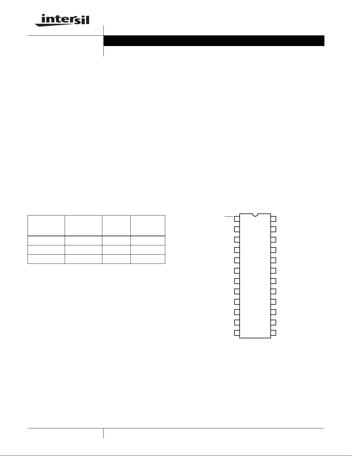
The EL5225 has 10 outputs, and is available in the 24-pin
TSSOP package. They are specified for operation over the
full -40°C to +85°C temperature range.
Ordering Information
PART
NUMBER
(See Note)
EL5225IRZ 24-Pin TSSOP - MDP0044
EL5225IRZ-T7 24-Pin TSSOP 7” MDP0044
EL5225IRZ-T13 24-Pin TSSOP 13” MDP0044
NOTE: Intersil Pb-free products employ special Pb-free material
sets; molding compounds/die attach materials and 100% matte tin
plate termination finish, which are RoHS compliant and compatible
with both SnPb and Pb-free soldering operations. Intersil Pb-free
products are MSL classified at Pb-free peak reflow temperatures that
meet or exceed the Pb-free requirements of IPC/JEDEC J STD-020C.
PACKAGE
(Pb-Free)
TAPE &
REEL PKG. DWG. #
Features
• 10-channel reference outputs
• Accuracy of ±1%
• Supply voltage of 5V to 16.5V
• Digital supply 3.3V to 5V
• Low supply current of 9mA
• Rail-to-rail capability
• Pb-free available (RoHS compliant)
Applications
• TFT-LCD drive circuits
• Reference voltage generators
Pinout
EL5225
(24-PIN TSSOP)
TOP VIEW
1
ENA OUTA
2
SDI
3
SCLK
4
SDO
VS+
VSD
REFH
REFL
5
6
7
8
9
EXT_OSC
24
23
22
21
20
19
18
17
16
FN7356.0
OUTB
OUTC
GND
OUTD
OUTE
OUTF
OUTG
GND
10
VS+
11
GND
12
CAP
1
Copyright © Intersil Americas Inc. 2002-2004. All Rights Reserved. Elantec is a registered trademark of Elantec Semiconductor, Inc.
CAUTION: These devices are sensitive to electrostatic discharge; follow proper IC Handling Procedures.
1-888-INTERSIL or 321-724-7143
| Intersil (and design) is a registered trademark of Intersil Americas Inc.
All other trademarks mentioned are the property of their respective owners.
15
14
13
OUTH
OUTI
OUTJ
EL5225
Absolute Maximum Ratings (T
Supply Voltage between V
Supply Voltage between V
Maximum Continuous Output Current . . . . . . . . . . . . . . . . . . . 30mA
& GND. . . . . . . . 4.5V (min) to 18V (max)
S
& GND . . 3V (min) to VS and 7V (max)
SD
= 25°C)
A
Maximum Die Temperature . . . . . . . . . . . . . . . . . . . . . . . . . . +125°C
Storage Temperature . . . . . . . . . . . . . . . . . . . . . . . .-65°C to +150°C
Ambient Operating Temperature . . . . . . . . . . . . . . . . -40°C to +85°C
Power Dissipation . . . . . . . . . . . . . . . . . . . . . . . . . . . . . See Curves
CAUTION: Stresses above those listed in “Absolute Maximum Ratings” may cause permanent damage to the device. This is a stress only rating and operation of the
device at these or any other conditions above those indicated in the operational sections of this specification is not implied.
IMPORTANT NOTE: All parameters having Min/Max specifications are guaranteed. Typ values are for information purposes only. Unless otherwise noted, all tests are
at the specified temperature and are pulsed tests, therefore: T
Electrical Specifications V
= 15V, V
S
otherwise specified.
SD
= TC = T
J
= 5V, V
REFH
A
= 13V, V
= 2V, RL = 1.5kΩ and CL = 200pF to 0V, TA = 25°C, unless
REFL
PARAMETER DESCRIPTION CONDITIONS MIN TYP MAX UNIT
SUPPLY
I
S
I
SD
Supply Current No load 9 11.5 mA
Digital Supply Current 0.17 0.35 mA
ANALOG
V
OL
V
OH
I
SC
PSRR Power Supply Rejection Ratio V
t
D
V
AC
∆V
MIS
V
DROOP
R
INH
REG Load Regulation I
Output Swing Low Sinking 5mA (V
Output Swing High Sourcing 5mA (V
REFH
REFH
= 15V, V
= 15V, V
= 0) 50 150 mV
REFL
= 0) 14.85 14.95 V
REFL
Short Circuit Current RL = 10Ω 100 140 mA
+ is moved from 14V to 16V 45 65 dB
S
Program to Out Delay 4ms
Accuracy referred to the ideal value Code = 512 20 mV
Channel to Channel Mismatch Code = 512 2 mV
Droop Voltage 12mV/ms
Input Resistance @ V
REFH
, V
REFL
32 kΩ
= 5mA step 0.5 1.5 mV/mA
OUT
CAP Band Gap Bypass with 0.1µF 1 1.3 1.6 V
DIGITAL
V
IH
F
CLK
V
IL
t
S
t
H
t
LC
t
CE
t
DCO
R
SDIN
T
PULSE
Logic 1 Input Voltage VSD = 5V 4 V
= 3.3V 2 V
V
SD
Clock Frequency 5MHz
Logic 0 Input Voltage VSD = 3.3V/5V 1 V
Setup Time 20 ns
Hold Time 20 ns
Load to Clock Time 20 ns
Clock to Load Line 20 ns
Clock to Out Delay Time Negative edge of SCLK 10 ns
S
Input Resistance 1GΩ
DIN
Minimum Pulse Width for EXT_OSC
5µs
Signal
Duty Cycle Duty Cycle for EXT_OSC Signal 50 %
INL Integral Nonlinearity Error 1.3 LSB
DNL Differential Nonlinearity Error 0.5 LSB
F_OSC Internal Refresh Oscillator Frequency OSC_Select = 0 21 kHz
2
FN7356.0
March 11, 2004
EL5225
Pin Descriptions
PIN NUMBER PIN NAME PIN TYPE PIN FUNCTION
1ENA
2 SDI Logic Input Serial data input
3 SCLK Logic Input Serial data clock
4 SDO Logic Output Serial data output
5 EXT_OSC Logic Input/Output External oscillator input or internal oscillator output
6, 10 VS+ Analog Power Positive supply voltage for analog circuits
NC Not connected
7 VSD Digital Power Positive power supply for digital circuits (3.3V - 5V)
8 REFH Analog Reference Input High reference voltage
9 REFL Analog Reference Input Low reference voltage
11 GND Ground Ground
12 CAP Analog Bypass Pin Decoupling capacitor for internal reference generator, 0.1µF
13 OUTJ Analog Output Channel J programmable output voltage
14 OUTI Analog Output Channel I programmable output voltage
Logic Input Chip select, low enables data input to logic
15 OUTH Analog Output Channel H programmable output voltage
17 OUTG Analog Output Channel G programmable output voltage
18 OUTF Analog Output Channel F programmable output voltage
19 OUTE Analog Output Channel E programmable output voltage
20 OUTD Analog Output Channel D programmable output voltage
22 OUTC Analog Output Channel C programmable output voltage
23 OUTB Analog Output Channel B programmable output voltage
24 OUTA Analog Output Channel A programmable output voltage
OUTL Analog Output Channel L programmable output voltage
OUTK Analog Output Channel K programmable output voltage
16, 21 GND Power Ground
3
FN7356.0
March 11, 2004
Typical Performance Curves
EL5225
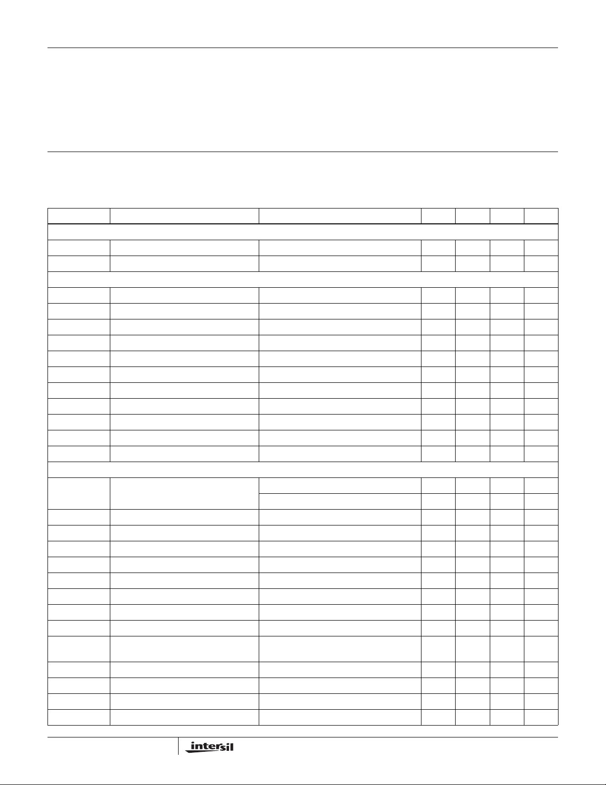
0.3
0.2
0.1
0
-0.1
-0.2
DIFFERENTIAL NONLINEARITY (LSB)
-0.3
10 210 410 610 810 1010
INPUT CODE
VS=15V
=5V
V
SD
V
REFH
V
REFL
=13V
=2V
1.5
1
0.5
0
INL (LSB)
-0.5
-1
0 200 400 600 800 1200
CODE
REFH=13V
REF
=2V
L
1000
FIGURE 1. DIFFERENTIAL NONLINEARITY vs CODE FIGURE 2. INTEGRAL NONLINEARITY ERROR
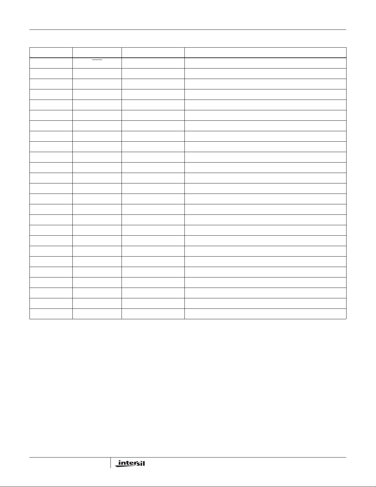
0mA
5mA
5V
CL=1nF
=20Ω
R
S
CL=4.7nF
=20Ω
R
S
5mA/DIV
200mV/DIV
5mA
0mA
CL=1nF
R
=20Ω
S
CL=4.7nF
R
=20Ω
S
CL=180pF
200mV/DIV
CL=180pF
M=400ns/DIV
VS=V
REFH
=15V
M=400ns/DIV
VS=V
REFH
=15V
FIGURE 3. TRANSIENT LOAD REGULATION (SOURCING) FIGURE 4. TRANSIENT LOAD REGULATION (SINKING)
5V
0V
5V
0V
10V
5V
0V
OUTPUT
M=400µs/DIV
SCLK
SDA
FIGURE 5. LARGE SIGNAL RESPONSE (RISING FROM 0V
TO 8V)
5V
0V
5V
0V
10V
5V
0V
OUTPUT
M=400µs/DIV
FIGURE 6. LARGE SIGNAL RESPONSE (FALLING FROM 8V
TO 0V)
SCLK
SDA
4
FN7356.0
March 11, 2004

Typical Performance Curves (Continued)
EL5225
5V
0V
5V
0V
200mV
OUTPUT
0V
M=400µs/DIV
SCLK
SDA
FIGURE 7. SMALL SIGNAL RESPONSE (RISING FROM 0V
TO 200mV)
JEDEC JESD51-7 HIGH EFFECTIVE THERMAL
CONDUCTIVITY TEST BOARD
1.4
1.176W
1.2
1
0.8
0.6
0.4
POWER DISSIPATION (W)
0.2
0
0 25 50 75 100 125
AMBIENT TEMPERATURE (°C)
T
S
S
θ
O
J
A
P
=
2
8
4
5
°
C
/
W
85
5V
0V
5V
0V
200mV
0V
OUTPUT
M=400µs/DIV
SCLK
SDA
FIGURE 8. SMALL SIGNAL RESPONSE (FALLING FROM
200mV TO 0V)
JEDEC JESD51-3 LOW EFFECTIVE THERMAL
CONDUCTIVITY TEST BOARD
0.9
781mW
0.8
0.7
0.6
0.5
0.4
0.3
0.2
POWER DISSIPATION (W)
0.1
0
0 25 50 75 100 125
T
S
θ
S
J
O
A
P
=
1
2
2
4
8
°
C
/
W
85
AMBIENT TEMPERATURE (°C)
FIGURE 9. POWER DISSIPATION vs AMBIENT
TEMPERATURE
General Description
The EL5225 provides a versatile method of providing the
reference voltages that are used in setting the transfer
characteristics of LCD display panels. The V/T
(Voltage/Transmission) curve of the LCD panel requires that
a correction is applied to make it linear; however, if the panel
is to be used in more than one application, the final curve
may differ for different applications. By using the EL5225,
the V/T curve can be changed to optimize its characteristics
according to the required application of the display product.
Each of the eight reference voltage outputs can be set with a
10-bit resolution. These outputs can be driven to within
50mV of the power rails of the EL5225. As all of the output
buffers are identical, it is also possible to use the EL5225 for
applications other than LCDs where multiple voltage
references are required that can be set to 10 bit accuracy.
5
FIGURE 10. POWER DISSIPATION vs AMBIENT
TEMPERATURE
Digital Interface
The EL5225 uses a simple 3-wire SPI compliant digital
interface to program the outputs. The EL5225 can support
the clock rate up to 5MHz.
Serial Interface
The EL5225 is programmed through a three-wire serial
interface. The start and stop conditions are defined by the
ENA
signal. While the ENA is low, the data on the SDI (serial
data input) pin is shifted into the 16-bit shift register on the
positive edge of the SCLK (serial clock) signal. The MSB (bit
15) is loaded first and the LSB (bit 0) is loaded last (see
Table 1). After the full 16-bit data has been loaded, the ENA
is pulled high and the addressed output channel is updated.
The SCLK is disabled internally when the ENA
SCLK must be low before the ENA
is pulled low.
is high. The
FN7356.0
March 11, 2004

EL5225
To facilitate the system designs that use multiple EL5225
chips, a buffered serial output of the shift register (SDO pin)
is available. Data appears on the SDO pin at the 16th falling
SCLK edge after being applied to the SDI pin.
To control the multiple EL5225 chips from a single three-wire
serial port, just connect the ENA
pins and the SCLK pins
together, connect the SDO pin to the SDI pin on the next
chip. While the ENA
is held low, the 16m-bit data is loaded to
the SDI input of the first chip. The first 16-bit data will go to
the last chip and the last 16-bit data will go to the first chip.
While the ENA
is held high, all addressed outputs will be
updated simultaneously.
The Serial Timing Diagram and parameters table show the
timing requirements for three-wire signals.
The serial data has a minimum length of 16 bits, the MSB
(most significant bit) is the first bit in the signal. The bits are
allocated to the following functions (also refer to the Control
Bits Logic Table)
• Bit 15 is always set to a zero
• Bit 14 controls the source of the clock, see the next
section for details
• Bits 13 through 10 select the channel to be written to,
these are binary coded with channel A = 0, and channel
H= 7
• The 10-bit data is on bits 9 through 0. Some examples of
data words are shown in the table of Serial Programming
Examples
TABLE 1. CONTROL BITS LOGIC TABLE
BIT NAME DESCRIPTION
B15 Test Always 0
B14 Oscillator 0 = Internal, 1 = External
B13 A3 Channel Address
B12 A2 Channel Address
B11 A1 Channel Address
B10 A0 Channel Address
B9 D9 Data
B8 D8 Data
B7 D7 Data
B6 D6 Data
B5 D5 Data
B4 D4 Data
B3 D3 Data
B2 D2 Data
B1 D1 Data
B0 D0 Data
Serial Timing Diagram
ENA
t
HE
SCLK
SDI
t
SD
t
SE
t
HD
B15 B14 B13 B12-B2 B1 B0
MSB LSB
Load MSB first, LSB last
Tt
r
t
w
t
f
t
HE
t
SE
t
6
FN7356.0
March 11, 2004

EL5225
TABLE 2. SERIAL TIMING PARAMETERS
PARAMETER RECOMMENDED OPERATING RANGE DESCRIPTION
T ≥200ns Clock Period
t
r/tf
t
HE
t
SE
t
HD
t
SD
t
W
TABLE 3. SERIAL PROGRAMMING EXAMPLES
CONTROL CHANNEL ADDRESS DATA
0 0 00000000000000Internal Oscillator, Channel A, Value = 0
0 0 00001111111111Internal Oscillator, Channel A, Value = 1023
0 0 00001000000000Internal Oscillator, Channel A, Value = 512
0 0 00111000000001‘tInternal Oscillator, Channel C, Value = 513
0 0 01110000011111Internal Oscillator, Channel H, Value = 31
0 1 01110000011111External Oscillator, Channel H, Value = 31
0.05 * T Clock Rise/Fall Time
≥10ns ENA Hold Time
≥10ns ENA Setup Time
≥10ns Data Hold Time
≥10ns Data Setup Time
0.50 * T Clock Pulse Width
CONDITIONC1 C0 A3 A2 A1 A0 D9 D8 D7 D6 D5 D4 D3 D2 D1 D0
Analog Section
TRANSFER FUNCTION
The transfer function is:
data
V
OUT IDEAL )(
V
=
where data is the decimal value of the 10-bit data binary
input code.
The output voltages from the EL5225 will be derived from
the reference voltages present at the V
pins. The impedance between those two pins is about 32kΩ.
Care should be taken that the system design holds these two
reference voltages within the limits of the power rails of the
EL5225. GND < V
In some LCD applications that require more than 10
channels, the system can be designed such that one
EL5225 will provide the Gamma correction voltages that are
more positive than the V
can provide the Gamma correction voltage more negative
than the V
potential. The Application Drawing shows a
COM
system connected in this way.
------------ -
REFL
1024
≤ VS and GND ≤ V
REFH
COM
V
REFH
- V
REFL
REFL
and V
REFL
≤ V
REFH
REFH
.
()×+
potential. The second EL5225
CLOCK OSCILLATOR
The EL5225 requires an internal clock or external clock to
refresh its outputs. The outputs are refreshed at the falling OSC
clock edges. The output refreshed switches open at the rising
edges of the OSC clock. The driving load shouldn’t be changed
at the rising edges of the OSC clock. Otherwise, it will generate
a voltage error at the outputs. This clock may be input or output
via the clock pin labeled OSC. The internal clock is provided by
an internal oscillator running at approximately 21kHz and can
be output to the OSC pin. In a 2 chip system, if the driving loads
are stable, one chip may be programmed to use the internal
oscillator; then the OSC pin will output the clock from the
internal oscillator. The second chip may have the OSC pin
connected to this clock source.
For transient load application, the external clock Mode
should be used to ensure all functions are synchronized
together. The positive edge of the external clock to the OSC
pin should be timed to avoid the transient load effect. The
Application Drawing shows the LCD H rate signal used, here
the positive clock edge is timed to avoid the transient load of
the column driver circuits.
After power on, the chip will start with the internal oscillator
mode. At this time, the OSC pin will be in a high impedance
condition to prevent contention. By setting B14 to high, the
chip is on external clock mode. Setting B14 to low, the chip is
on internal clock mode.
7
FN7356.0
March 11, 2004

Block Diagram
EIGHT
CHANNEL
MEMORY
EL5225
REFERENCE HIGH
OUTA
OUTB
OUTH
VOLTAGE
SOURCES
OUTI
OUTJ
REFERENCE LOW
CLK
SDI
LOAD
FILTER
CONTROL IF
CHANNEL OUTPUTS
Each of the channel outputs has a rail-to-rail buffer. This
enables all channels to have the capability to drive to within
50mV of the power rails, (see Electrical Characteristics for
details).
When driving large capacitive loads, a series resistor should
be placed in series with the output. (Usually between 5Ω and
50Ω).
Each of the channels is updated on a continuous cycle, the
time for the new data to appear at a specific output will
depend on the exact timing relationship of the incoming data
to this cycle.
The best-case scenario is when the data has just been
captured and then passed on to the output stage
immediately; this can be as short as 48µs. In the worst-case
scenario, this will be 480µs when the data has just missed
the cycle.
When a large change in output voltage is required, the
change will occur in 2V steps, thus the requisite number of
timing cycles will be added to the overall update time. This
means that a large change of 16V can take between 3.8ms
REFERENCE DECOUPLE
SDO
EXT_OSC
and 4.2ms depending on the absolute timing relative to the
update cycle.
Output Stage and the Use of External Oscillator
Simplified output sample and hold amp stage for one
channel.
CH
S
1.3V
V
+
-
+
IN
-
The output voltage is generated from the DAC, which is V
at the above circuit. The refreshed switches are controlled
by the internal or external oscillator signal. When the OSC
clock signal is low, the switch S
output V
= VIN and at the same time the sample and
OUT
hold cap CH is being charged. When the OSC clock signal is
high, the refreshed switch S
output voltage is maintained by CH. This refreshed process
1
FIGURE 11.
and S2 are opened and the
1
+
1.3V
-
S
2
OSC
and S2 are closed. The
1
V
OUT
IN
8
FN7356.0
March 11, 2004

will repeat every 10-clock cycles for each channel. The time
takes to update the output depends on the timing at the V
IN
and the state of the switches. It can take 1 to 10 clock cycles
to update each output.
EL5225
V
OUT1
For the sample and hold capacitor CH to maintain the
correct output voltage, the driving load shouldn’t be changed
at the rising edge of the OSC signal. Since at the rising edge
of the OSC clock, the refreshed switches are being opened,
if the load changes at that time, it will generate an error
output voltage. For a fixed load condition, the internal
oscillator can be used.
For the transient load condition, the external OSC mode
should be used to avoid the conflict between the rising edge
of the OSC signal and the changing load. So a timing delay
circuit will be needed to delay the OSC signal and avoid the
rising edge of the OSC signal and changing the load at the
same time.
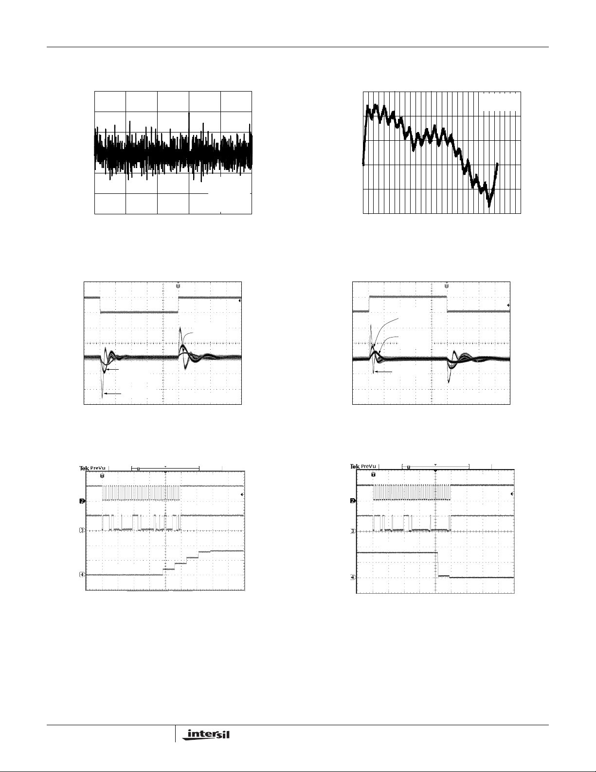
I
OUT
V
OUT
OSC
M=400µs/DIV
OSC
V
OUT2
M=400µs/DIV
FIGURE 13. CHANNEL-TO-CHANNEL REFRESH
Ch1 - Output1
Ch3 - Output2
Ch2 - EXT_OSC
At the falling edge of the OSC, output 1 is refreshing and one
clock cycle later, output2 is being refreshed. The spike you
see here is the response of the output amplifier when the
refreshed switches are closed. When driving a big capacitor
load, there will be ringing at the spikes because the phase
margin of the amplifier is decreased.
The speed of the external OSC signal shouldn’t be greater
than 70kHz because for the worst condition, it will take at
least 4µs to charge the sample and hold Capacitor CH. The
pulse width has to be at least 4µs long. From our lab test, the
duty cycle of the OSC signal must be greater than 30%.
FIGURE 12. TRANSIENT LOAD RESPONSE
Channel 3 - sinking and sourcing 5mA current
Channel 2 - EXT_OSC signal
Channel 1 - V
OUT
Here, the OSC signal is synchronized to the load signal. The
rising edge of the OSC signal is then delayed by some
amount of time and gives enough time for CH to be charged
to a new voltage before the switches are opened.
POWER DISSIPATION
With the 30mA maximum continues output drive capability
for each channel, it is possible to exceed the 125°C absolute
maximum junction temperature. Therefore, it is important to
calculate the maximum junction temperature for the
application to determine if load conditions need to be
modified for the part to remain in the safe operation.
The maximum power dissipation allowed in a package is
determined according to:
P
DMAX
JMAX
---------------------------------------------
=
AMAX
Θ
JA
T
- T
where:
•T
•T
• θ
•P
= Maximum junction temperature
JMAX
= Maximum ambient temperature
AMAX
= Thermal resistance of the package
JA
= Maximum power dissipation in the package
DMAX
9
FN7356.0
March 11, 2004

EL5225
The maximum power dissipation actually produced by the IC
is the total quiescent supply current times the total power
supply voltage and plus the power in the IC due to the loads.
P
DMAXVSIS
Σ VS( - V
OUT
i ) I
LOAD
i×[]+×=
when sourcing, and:
P
DMAXVSIS
Σ V
OUT
iI
LOAD
i×()+×=
when sinking.
Where:
• i = 1 to total 10
•V
= Supply voltage
S
= Quiescent current
•I
S
•V
•I
By setting the two P
can solve for the R
i = Output voltage of the i channel
OUT
i = Load current of the i channel
LOAD
equations equal to each other, we
DMAX
s to avoid the device overheat. The
LOAD
package power dissipation curves provide a convenient way
to see if the device will overheat.
POWER SUPPLY BYPASSING AND PRINTED CIRCUIT
BOARD LAYOUT
Good printed circuit board layout is necessary for optimum
performance. A low impedance and clean analog ground
plane should be used for the EL5225. The traces from the
two ground pins to the ground plane must be very short.
Lead length should be as short as possible and all power
supply pins must be well bypassed. A 0.1µF ceramic
capacitor must be place very close to the V
V
, and CAP pins. A 4.7µF local bypass tantalum
REFL
capacitor should be placed to the V
, V
S
REFH
, V
S
, and V
REFH
,
REFL
pins.
APPLICATION USING THE EL5225
In the first application drawing, the schematic shows the
interconnect of a pair of EL5225 chips connected to give
10 gamma corrected voltages above the V
10 gamma corrected voltages below the V
voltage, and
COM
voltage.
COM
10
FN7356.0
March 11, 2004

Application Drawing
MICROCONTROLLER
LCD
TIMING
CONTROLLER
HORIZONTAL
RATE
HIGH REFERENCE
VO LTAGE
+10V
+12V
+5V
0.1µF
EL5225
0.1µF
0.1µF
0.1µF
REFH
VS
VSD
SDI
SCK
ENA
SDO
OSC
CAP
REFL
OUTA
OUTB
OUTC
OUTD
OUTE
OUTF
OUTI
COLUMN
(SOURCE)
DRIVER
LCD PANEL
+5.5V
LOW REFERENCE
VO LTAGE
+1V
+12V
+5V
0.1µF
GND
EL5225
MIDDLE REFERENCE VOLTAGE
REFH
OSC
VS
0.1µF
VSD
SDI
SCK
ENA
CAP
0.1µF
REFL
0.1µF
GND
EL5225
OUTJ
OUTA
OUTB
OUTC
OUTD
OUTE
OUTF
OUTI
OUTJ
11
FN7356.0
March 11, 2004

TSSOP Package Outline Drawing
EL5225
NOTE: The package drawing shown here may not be the latest version. To check the latest revision, please refer to the Intersil
website at <http://www.intersil.com/design/packages/index.asp>
All Intersil U.S. products are manufactured, assembled and tested utilizing ISO9000 quality systems.
Intersil Corporation’s quality certifications can be viewed at www.intersil.com/design/quality
Intersil products are sold by description only. Intersil Corporation reserves the right to make changes in circuit design, software and/or specifications at any time without
notice. Accordingly, the reader is cautioned to verify that data sheets are current before placing orders. Information furnished by Intersil is believed to be accurate and
reliable. However, no responsibility is assumed by Intersil or its subsidiaries for its use; nor for any infringements of patents or other rights of third parties which may result
from its use. No license is granted by implication or otherwise under any patent or patent rights of Intersil or its subsidiaries.
For information regarding Intersil Corporation and its products, see www.intersil.com
12
FN7356.0
March 11, 2004
 Loading...