

®
R
T
O
N
E
M
M
O
C
E
E
E
S
O
F
D
E
D
N
6
1
5
L
E
5
6
1
5
L
E
/
4
W
E
N
R
Data Sheet August 3, 2005
EL5192, EL5192A
FN7181.2
S
N
G
I
S
E
D
600MHz Current Feedback Amplifier with
Enable
The EL5192 and EL5192A are current feedback amplifiers
with a very high bandwidth of 600MHz. This makes these
amplifiers ideal for today’s high speed video and monitor
applications.
With a supply current of just 6mA and the ability to run from
a single supply voltage from 5V to 10V, the amplifiers are
also ideal for hand held, portable or battery-powered
equipment.
The EL5192A also incorporates an enable and disable
function to reduce the supply current to 100µA typical per
amplifier. Allowing the CE
pin to float or applying a low logic
level will enable the amplifier.
The EL5192 is offered in the 5-pin SOT-23 package and the
EL5192A is available in the 6-pin SOT-23 as well as the
industry-standard 8-pin SO packages. Both operate over the
industrial temperature range of -40°C to +85°C.
Ordering Information
PART NUMBER PACKAGE TAPE & REEL PKG. DWG. #
EL5192CW-T7 5-Pin SOT-23 7” (3K pcs) MDP0038
EL5192CW-T7A 5-Pin SOT-23 7” (250 pcs) MDP0038
EL5192CWZ-T7
(See Note)
EL5192CWZ-T7A
(See Note)
EL5192ACW-T7 6-Pin SOT-23 7” (3K pcs) MDP0038
EL5192ACW-T7A 6-Pin SOT-23 7”(250 pcs) MDP0038
EL5192ACWZ-T7
(See Note)
EL5192ACWZ-T7A
(See Note)
EL5192ACS 8-Pin SO - MDP0027
EL5192ACS-T7 8-Pin SO 7” MDP0027
EL5192ACS-T13 8-Pin SO 13” MDP0027
EL5192ACSZ
(See Note)
EL5192ACSZ-T7
(See Note)
EL5192ACSZ-T13
(See Note)
NOTE: Intersil Pb-free plus anneal products employ special Pb-free material
sets; molding compounds/die attach materials and 100% matte tin plate
termination finish, which are RoHS compliant and compatible with both SnPb
and Pb-free soldering operations. Intersil Pb-free products are MSL classified
at Pb-free peak reflow temperatures that meet or exceed the Pb-free
requirements of IPC/JEDEC J STD-020.
5-Pin SOT-23
(Pb-free)
5-Pin SOT-23
(Pb-free)
6-Pin SOT-23
(Pb-free)
6-Pin SOT-23
(Pb-free)
8-Pin SO
(Pb-free)
8-Pin SO
(Pb-free)
8-Pin SO
(Pb-free)
7” (3K pcs) MDP0038
7” (250 pcs) MDP0038
7” (3K pcs) MDP0038
7”(250 pcs) MDP0038
- MDP0027
7” MDP0027
13” MDP0027
Features
• 600MHz -3dB bandwidth
• 6mA supply current
• Single and dual supply operation, from 5V to 10V supply
span
• Fast enable/disable (EL5192A only)
• Available in SOT-23 packages
• Dual (EL5292) and triple (EL5392) available
• High speed, 1GHz product available (EL5191)
• Low power, 4mA, 300MHz product available (EL5193,
EL5293, and EL5393)
• Pb-Free plus anneal available (RoHS compliant)
Applications
• Video amplifiers
• Cable drivers
• RGB amplifiers
• Test equipment
• Instrumentation
• Current to voltage converters
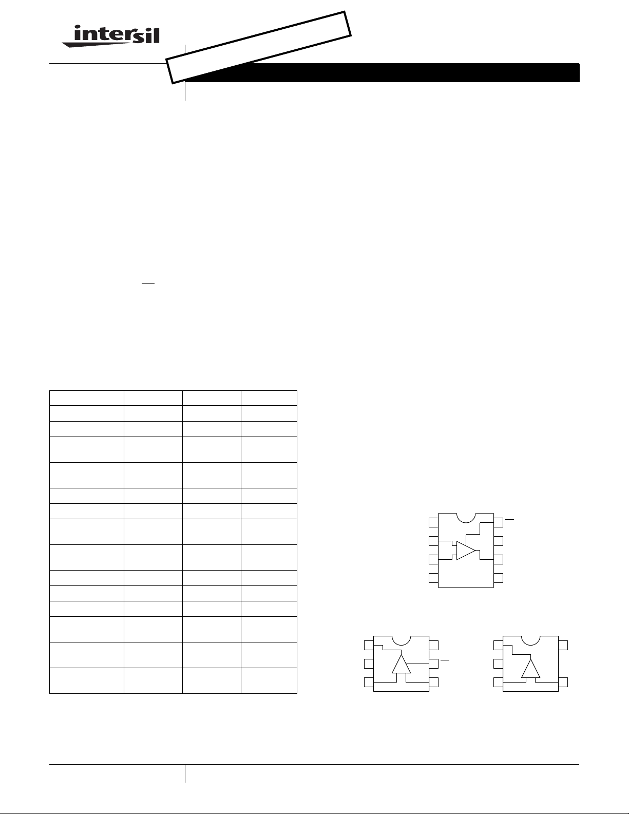
Pinouts
EL5192A
(8-PIN SO)
TOP VIEW
(6-PIN SOT-23)
1
OUT
2
VS-
3
IN+
EL5192A
TOP VIEW
-+
NC
IN-
IN+
VS-
1
2
3
4
6
VS+
5 CE
4
IN-
-
+
8
CE
7
VS+
6
OUT
5
NC
(5-PIN SOT-23)
1
OUT
2
VS-
3
IN+
EL5192
TOP VIEW
-+
5
4
VS+
IN-
1
CAUTION: These devices are sensitive to electrostatic discharge; follow proper IC Handling Procedures.
1-888-INTERSIL or 1-888-468-3774
| Intersil (and design) is a registered trademark of Intersil Americas Inc.
Copyright Intersil Americas Inc. 2004, 2005. All Rights Reserved
All other trademarks mentioned are the property of their respective owners.
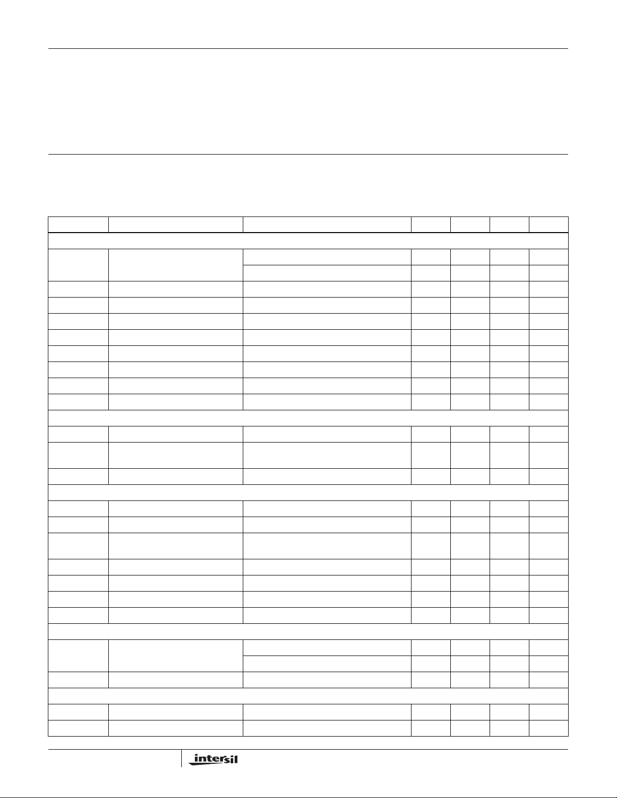
EL5192, EL5192A
Absolute Maximum Ratings (T
Supply Voltage between V
Maximum Continuous Output Current . . . . . . . . . . . . . . . . . . . 50mA
Operating Junction Temperature. . . . . . . . . . . . . . . . . . . . . . .125°C
+ and VS-. . . . . . . . . . . . . . . . . . . . .11V
S
= 25°C)
A
Pin Voltages. . . . . . . . . . . . . . . . . . . . . . . . . V
Storage Temperature. . . . . . . . . . . . . . . . . . . . . . . .-65°C to +150°C
- -0.5V to VS+ +0.5V
S
Ambient Operating Temperature. . . . . . . . . . . . . . . .-40°C to +85°C
Power Dissipation . . . . . . . . . . . . . . . . . . . . . . . . . . . . . See Curves
CAUTION: Stresses above those listed in “Absolute Maximum Ratings” may cause permanent damage to the device. This is a stress only rating and operation of the
device at these or any other conditions above those indicated in the operational sections of this specification is not implied.
IMPORTANT NOTE: All parameters having Min/Max specifications are guaranteed. Typical values are for information purposes only. Unless otherwise noted, all tests
are at the specified temperature and are pulsed tests, therefore: TJ = TC = T
Electrical Specifications V
+ = +5V, VS- = -5V, RF = 750Ω for AV = 1, RF = 375Ω for AV = 2, RL = 150Ω, TA = 25°C unless otherwise
S
A
specified.
PARAMETER DESCRIPTION CONDITIONS MIN TYP MAX UNIT
AC PERFORMANCE
BW -3dB Bandwidth A
= +1 600 MHz
V
AV = +2 300 MHz
BW1 0.1dB Bandwidth 25 MHz
SR Slew Rate V
t
S
e
N
i
- IN- Input Current Noise 20 pA/√Hz
N
i
+ IN+ Input Current Noise 50 pA/√Hz
N
0.1% Settling Time V
Input Voltage Noise 4.1 nV/√Hz
= -2.5V to +2.5V, AV = +2 2400 2800 V/µs
O
= -2.5V to +2.5V, AV = -1 9 ns
OUT
dG Differential Gain Error (Note 1) AV = +2 0.015 %
dP Differential Phase Error (Note 1) A
= +2 0.04 °
V
DC PERFORMANCE
V
OS
T
CVOS
Offset Voltage -10 1 10 mV
Input Offset Voltage Temperature
Measured from T
MIN
to T
MAX
5µV/°C
Coefficient
R
OL
Transimpedance 200 400 kΩ
INPUT CHARACTERISTICS
CMIR Common Mode Input Range ±3 ±3.3 V
CMRR Common Mode Rejection Ratio 42 50 dB
-ICMR - Input Current Common Mode
-6 6 µA/V
Rejection
+I
IN
-I
IN
R
IN
C
IN
+ Input Current -60 3 60 µA
- Input Current -35 2 35 µA
Input Resistance 37 kΩ
Input Capacitance 0.5 pF
OUTPUT CHARACTERISTICS
V
I
OUT
O
Output Voltage Swing RL = 150Ω to GND ±3.4 ±3.7 V
= 1kΩ to GND ±3.8 ±4.0 V
R
L
Output Current RL =10Ω to GND 95 120 mA
SUPPLY
I
SON
I
SOFF
Supply Current - Enabled No load, V
Supply Current - Disabled No load, V
= 0V 5 6 7.5 mA
IN
= 0V 100 150 µA
IN
2
EL5192, EL5192A
Electrical Specifications V
+ = +5V, VS- = -5V, RF = 750Ω for AV = 1, RF = 375Ω for AV = 2, RL = 150Ω, TA = 25°C unless otherwise
S
specified. (Continued)
PARAMETER DESCRIPTION CONDITIONS MIN TYP MAX UNIT
PSRR Power Supply Rejection Ratio DC, V
-IPSR - Input Current Power Supply
= ±4.75V to ±5.25V 55 75 dB
S
DC, V
= ±4.75V to ±5.25V -2 2 µA/V
S
Rejection
ENABLE (EL5192A ONLY)
t
EN
t
DIS
I
IHCE
I
ILCE
V
IHCE
V
ILCE
Enable Time 40 ns
Disable Time 600 ns
CE Pin Input High Current CE = VS+0.86µA
CE Pin Input Low Current CE = VS-0-0.1µA
CE Input High Voltage for Power-
VS+ -1 V
down
CE Input Low Voltage for Power-
VS+ -3 V
down
NOTE:
1. Standard NTSC test, AC signal amplitude = 286mV
, f = 3.58MHz
P-P
3
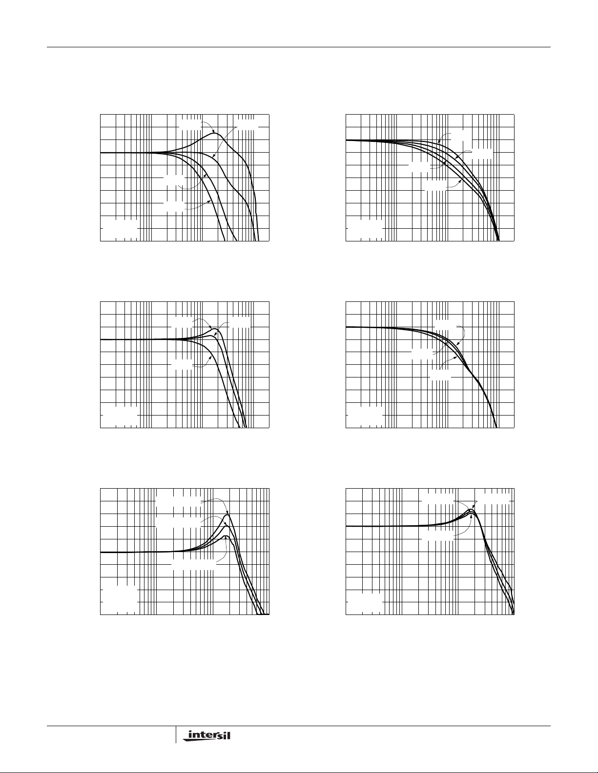
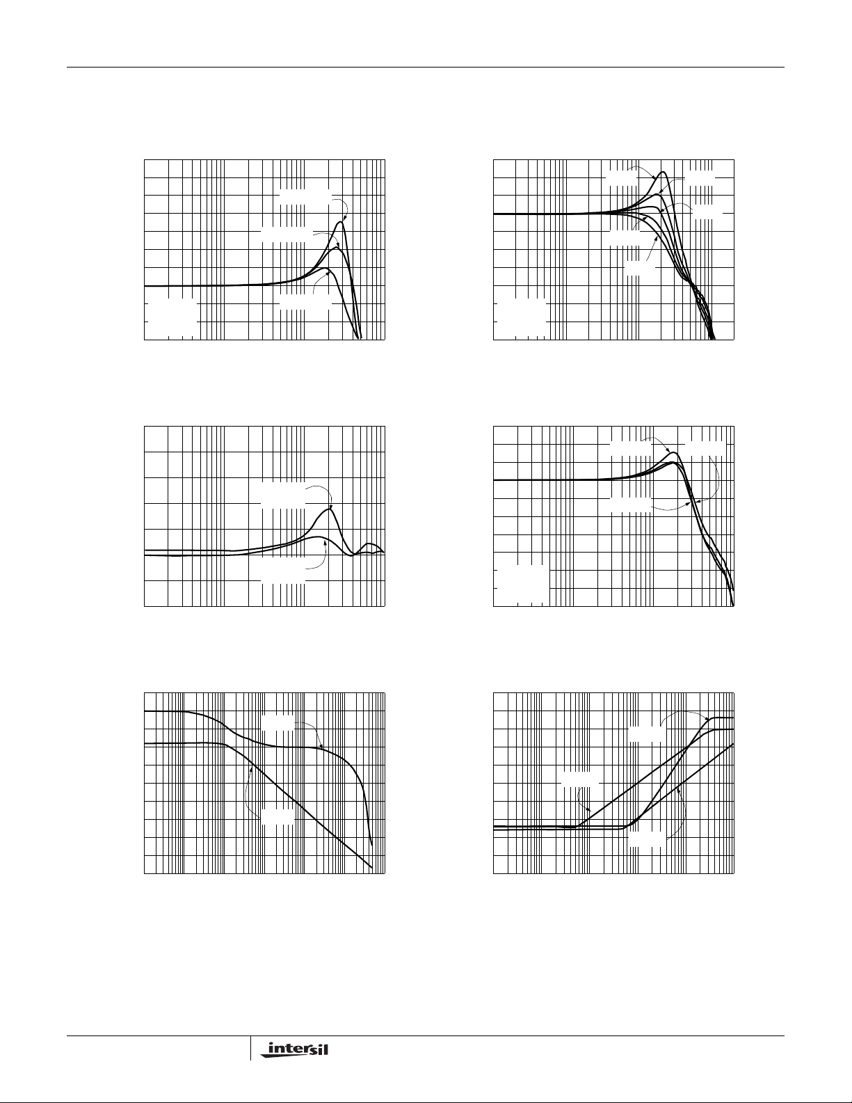
Typical Performance Curves
EL5192, EL5192A
Non-Inverting Frequency Response (Gain)
SOT-23 Package
6
AV=1
2
-2
AV=5
-6
Normalized Magnitude (dB)
-10
RF=750Ω
RL=150Ω
-14
1M 10M 100M 1G
Inverting Frequency Response (Gain)
6
2
-2
-6
AV=10
Frequency (Hz)
AV=-1 AV=-2
AV=-5
AV=2
Non-Inverting Frequency Response (Phase)
90
0
-90
Phase (°)
-180
-270
RF=750Ω
RL=150Ω
-360
1M 10M 100M 1G
Inverting Frequency Response (Phase)
90
0
-90
Phase (°)
-180
AV=5
AV=10
Frequency (Hz)
AV=-1
AV=-2
AV=-5
AV=1
AV=2
Normalized Magnitude (dB)
-10
RF=375Ω
RL=150Ω
-14
1M 10M 100M 1G
Frequency (Hz)
Frequency Response for Various CIN-
10
2pF added
6
2
-2
Normalized Magnitude (dB)
-6
AV=2
R
=375Ω
F
RL=150Ω
-10
1M 10M 1G
1pF added
0pF added
100M
Frequency (Hz)
-270
RF=375Ω
RL=150Ω
-360
1M 10M 100M 1G
Frequency (Hz)
Frequency Response for Various R
6
2
-2
-6
Normalized Magnitude (dB)
-10
AV=2
RF=375Ω
-14
1M 10M 100M 1G
Frequency (Hz)
L
RL=500Ω
RL=100ΩRL=150Ω
4
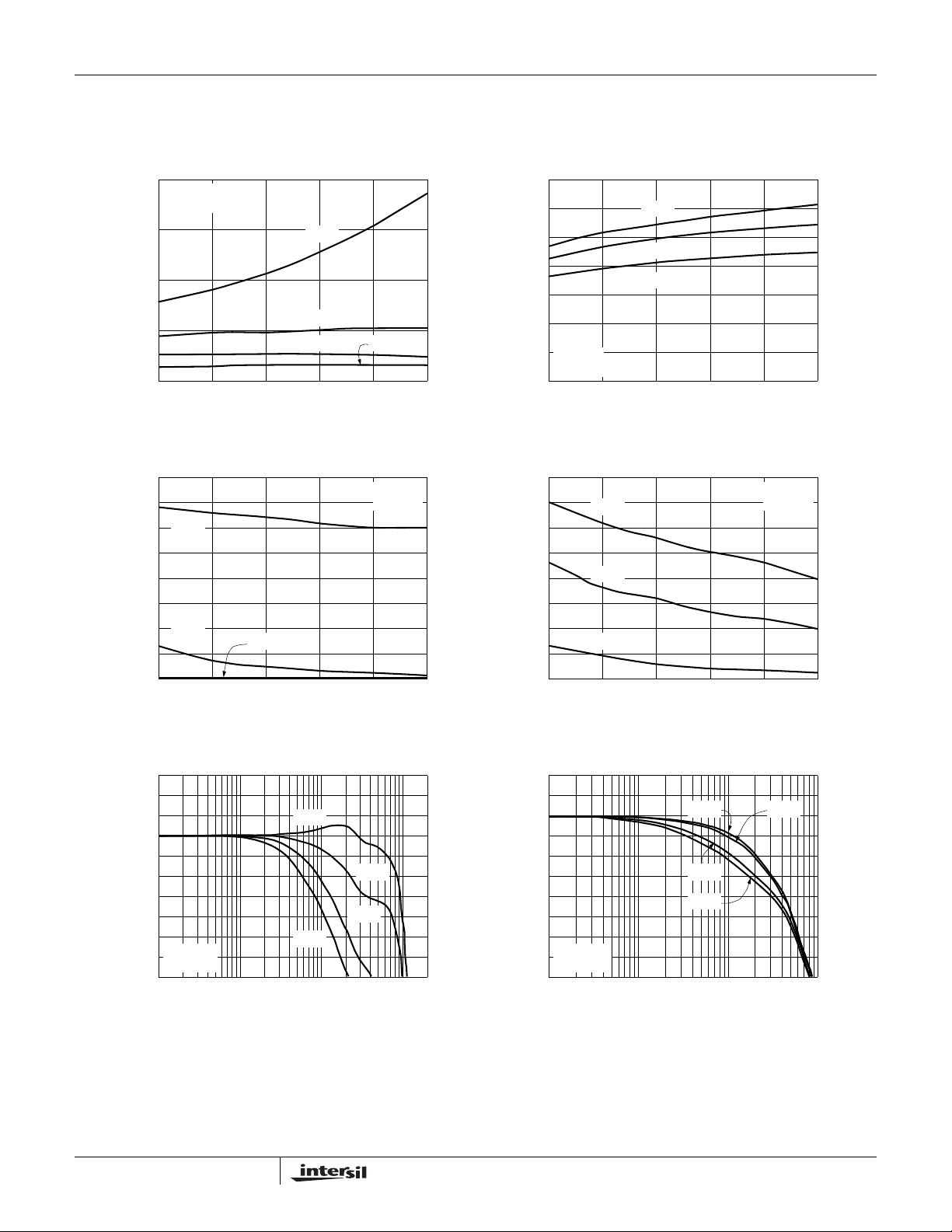
Typical Performance Curves (Continued)
EL5192, EL5192A
Frequency Response for Various C
14
10
6
2
Normalized Magnitude (dB)
-2
AV=2
RF=375Ω
RL=150Ω
-6
1M 10M 100M 1G
Frequency (Hz)
Group Delay vs Frequency
3.5
3
2.5
2
1.5
Group Delay (ns)
1
0.5
0
1M 10M 1G
Frequency (Hz)
L
12pF added
8pF added
0pF added
AV=2
RF=375Ω
AV=1
RF=750Ω
100M
Frequency Response for Various R
6
2
-2
-6
Normalized Magnitude (dB)
-10
AV=2
RG=R
F
RL=150Ω
-14
1M 10M 100M 1G
Frequency (Hz)
Frequency Response for Various Common-Mode Input
Voltages
6
2
-2
-6
Normalized Magnitude (dB)
-10
AV=2
RF=375Ω
RL=150Ω
-14
1M 10M 1G
Frequency (Hz)
F
250Ω 375Ω
620Ω
750Ω
VCM=3V VCM=0V
VCM=-3V
100M
475Ω
Transimpedance (ROL) vs Frequency
10M
1M
100k
10k
Magnitude (Ω)
1k
100
1k
10k 100k 1M 10M 100M 1G
Phase
Gain
Frequency (Hz)
5
0
-90
-180
-270
-360
PSRR and CMRR vs Frequency
20
0
-20
PSRR-
Phase (°)
-40
PSRR/CMRR (dB)
-60
-80
10k
100k 1M 10M 1G100M
Frequency (Hz)
PSRR+
CMRR
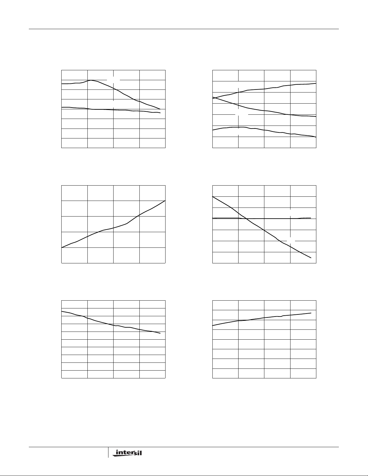
Typical Performance Curves (Continued)
EL5192, EL5192A
-3dB Bandwidth vs Supply Voltage for Non-Inverting Gains
800
RF=750Ω
=150Ω
R
L
600
400
-3dB Bandwidth (MHz)
200
0
567 10
Total Supply Voltage (V)
Peaking vs Supply Voltage for Non-Inverting Gains
4
3
AV=1
2
Peaking (dB)
1
AV=2
AV=10
AV=1
AV=2
AV=5 AV=10
89
RF=750Ω
RL=150Ω
-3dB Bandwidth vs Supply Voltage for Inverting Gains
350
300
250
200
150
100
-3dB Bandwidth (MHz)
50
RF=375Ω
RL=150Ω
0
567 1089
Peaking vs Supply Voltage for Inverting Gains
4
AV=-1
3
2
Peaking (dB)
1
AV=-2
AV=-5
AV=-1
AV=-2
AV=-5
Total Supply Voltage (V)
RF=375Ω
RL=150Ω
0
567 1089
Total Supply Voltage (V)
Non-inverting Frequency Response (Gain)
SO8 Package
6
2
-2
-6
Normalized Magnitude (dB)
-10
RF=750Ω
RL=150Ω
-14
1M 10M 100M 1.6G
AV=1
AV=2
AV=5
AV=10
Frequency (Hz)
1G
0
567 1089
Total Supply Voltage (V)
Non-inverting Frequency Response (Phase)
SO8 Package
90
0
-90
Phase (°)
-180
-270
RF=750Ω
RL=150Ω
-360
1M 10M 100M 1G
AV=1 AV=2
AV=5
AV=10
Frequency (Hz)
6

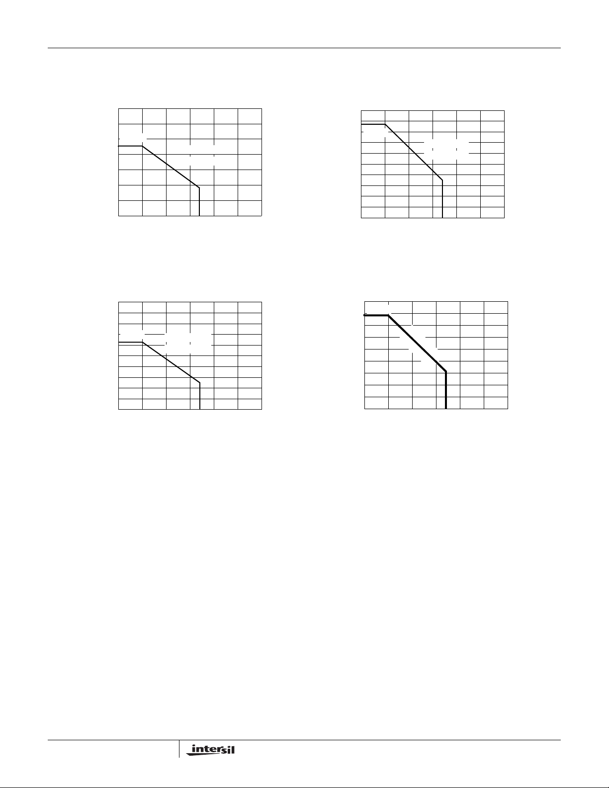
Typical Performance Curves (Continued)
EL5192, EL5192A
Inverting Frequency Response (Gain)
SO8 Package
6
2
-2
-6
Normalized Magnitude (dB)
-10
RF=375Ω
RL=150Ω
-14
1M 10M 100M 1G
-3dB Bandwidth vs Temperature for Non-Inverting Gains
1400
1200
1000
-3dB Bandwidth (MHz)
800
600
400
200
AV=1
AV=2
AV=-1
AV=-5
Frequency (Hz)
AV=5 AV=10
AV=-2
RF=750Ω
RL=150Ω
Inverting Frequency Response (Phase)
SO8 Package
90
0
-90
AV=-2
Phase (°)
-180
-270
RF=375Ω
RL=150Ω
-360
1M 10M 100M 1G
Frequency (Hz)
-3dB Bandwidth vs Temperature for Inverting Gains
500
AV=-1
AV=-2
AV=-5
-3dB Bandwidth (MHz)
400
300
200
100
AV=-1
AV=-5
RF=375Ω
RL=150Ω
0
-40 10 60 160
Ambient Temperature (°C)
Peaking vs Temperature
2
RL=150Ω
1.5
1
0.5
Peaking (dB)
0
-0.5
-50 0 50 100
-50
Ambient Temperature (°C)
AV=1
AV=-1
AV=-2
110
AV=2
Voltage Noise (nV/√Hz)
0
-40 10 60 160
Ambient Temperature (°C)
Voltage and Current Noise vs Frequency
1k
100
in-
10
Current Noise (pA/√Hz)
1
100
in+
e
n
1k 10k 100k 10M1M
Frequency (Hz)
110
7

Typical Performance Curves (Continued)
EL5192, EL5192A
Closed Loop Output Impedance vs Frequency
100
10
1
0.1
Output Impedance (Ω)
0.01
0.001
100 10k 100M 1G1M
2nd and 3rd Harmonic Distortion vs Frequency
-20
AV=+2
V
RL=100Ω
1
OUT
=2V
P-P
-30
-40
-50
-60
-70
-80
Harmonic Distortion (dBc)
-90
-100
100k 10M1k
Frequency (Hz)
2nd Order
Distortion
Frequency (MHz)
3rd Order
Distortion
10 100
Supply Current vs Supply Voltage
10
8
6
4
Supply Current (mA)
2
0
0
Supply Voltage (V)
Two-Tone 3rd Order
Input Referred Intermodulation Intercept (IIP3)
30
25
20
15
10
5
0
-5
Input Power Intercept (dBm)
-10
-15
10
AV=+2
RL=100Ω
Frequency (MHz)
12210864
AV=+2
RL=150Ω
100 200
Differential Gain/Phase vs DC Input
Voltage at 3.58MHz
0.03
AV=2
R
0.02
0.01
0
-0.01
-0.02
dG (%) or dP (°)
-0.03
-0.04
-0.05
=375Ω
F=RG
=150Ω
R
L
-1 -0.5 0 0.5 1
DC Input Voltage
8
dP
dG
Differential Gain/Phase vs DC Input
Voltage at 3.58MHz
0.03
AV=1
0.02
R
=750Ω
F
=500Ω
R
L
0.01
0
-0.01
-0.02
dG (%) or dP (°)
-0.03
-0.04
-0.05
-0.06
-1 -0.5 0 0.5 1
DC Input Voltage
dP
dG

Typical Performance Curves (Continued)
EL5192, EL5192A
)
PP
Output Voltage Swing (V
200mV/div
Output Voltage Swing vs Frequency
THD<1%
9
8
7
6
5
4
3
2
1
AV=2 AV=2
0
1
Small Signal Step Response Large Signal Step Response
RL=150Ω
Frequency (MHz)
RL=500Ω
10 100
VS=±5V
RL=150Ω
AV=2
RF=RG=375Ω
Output Voltage Swing vs Frequency
THD<0.1%
10
)
8
PP
Output Voltage Swing (V
1V/div
6
4
2
0
RL=150Ω RL=500Ω
1
10 100
Frequency (MHz)
VS=±5V
RL=150Ω
AV=2
RF=RG=375Ω
10ns/div
Settling Time vs Settling Accuracy
25
20
15
10
Settling Time (ns)
5
0
0.01 0.1 1
Settling Accuracy (%)
AV=2
R
F=RG
R
L
V
STEP
=150Ω
=375Ω
=5V
P-P
output
10ns/div
Transimpedance (RoI) vs Temperature
500
450
400
RoI (kΩ)
350
300
-40 10 60 110 160
Die Temperature (°C)
9
Typical Performance Curves (Continued)
EL5192, EL5192A
PSRR and CMRR vs Temperature
90
80
70
60
50
40
PSRR/CMRR (dB)
30
20
10
-40 10 60 110 160
Offset Voltage vs Temperature
3
2
1
(mV)
OS
0
V
-1
PSRR
CMRR
Die Temperature (°C)
ICMR and IPSR vs Temperature
2.5
2
1.5
1
0.5
ICMR/IPSR (µA/V)
0
-0.5
-1
-40 10 60 110 160
Input Current vs Temperature
60
40
20
0
-20
Input Current (µA)
-40
-60
ICMR+
IPSR
ICMR-
Die Temperature (°C)
IB-
IB+
-2
-40 10 60 110 160
Die Temperature (°C)
Positive Input Resistance vs Temperature
50
45
40
35
30
25
+ (kΩ)
IN
20
R
15
10
5
0
-40 10 160
Temperature (°C)
-80
-40 10 110 160
Supply Current vs Temperature
8
7
6
5
4
3
Supply Current (mA)
2
1
11060
0
-40 10 110 160
60
Temperature (°C)
60
Temperature (°C)
10

Typical Performance Curves (Continued)
EL5192, EL5192A
Positive Output Swing vs Temperature for Various Loads
4.2
4.1
4
3.9
(V)
OUT
3.8
V
3.7
3.6
3.5
-40 10 50 160
Output Current vs Temperature
135
130
125
(mA)
OUT
I
120
115
-40 10 60 110 160
1kΩ
150Ω
Temperature (°C)
Sink
Source
Die Temperature (°C)
110
Negative Output Swing vs Temperature for Various Loads
-3.5
-3.6
-3.7
-3.8
(V)
OUT
-3.9
V
-4
-4.1
-4.2
-40 10 110 160
Slew Rate vs Temperature
4600
4400
4200
4000
3800
3600
Slew Rate (V/µS)
3400
3200
3000
-40 10 60 110 160
150Ω
1kΩ
60
Temperature (°C)
Die Temperature (°C)
AV=2
RF=RG=375Ω
RL=150Ω
500mV/div
5V/div
Enable Response Disable Response
500mV/div
5V/div
20ns/div
11
400ns/div
Typical Performance Curves (Continued)
EL5192, EL5192A
JEDEC JESD51-7 HIGH EFFECTIVE
THERMAL CONDUCTIVITY TEST BOARD
1.4
1.2
909mW
1
0.8
0.6
0.4
0.2
POWER DISSIPATION (W)
0
0 255075100 150
AMBIENT TEMPERATURE (°C)
JEDEC JESD51-3 LOW EFFECTIVE
THERMAL CONDUCTIVITY TEST BOARD
1
0.9
0.8
0.7
625mW
0.6
0.5
0.4
0.3
0.2
POWER DISSIPATION (W)
0.1
0
0 255075100 150
AMBIENT TEMPERATURE (°C)
SO8
θJA=110°C/W
12585
SO8
θJA=160°C/W
12585
JEDEC JESD51-7 HIGH EFFECTIVE
THERMAL CONDUCTIVITY TEST BOARD
0.5
0.45
0.4
435mW
0.35
0.3
0.25
0.2
0.15
0.1
POWER DISSIPATION (W)
0.05
0
0 25 50 75 100 150
AMBIENT TEMPERATURE (°C)
JEDEC JESD51-3 LOW EFFECTIVE
THERMAL CONDUCTIVITY TEST BOARD
0.45
391mW
0.4
0.35
0.3
0.25
0.2
0.15
0.1
POWER DISSIPATION (W)
0.05
0
0 255075100 150
AMBIENT TEMPERATURE (°C)
S
θ
J
A
=
2
SOT23-5/6
θJA=230°C/W
85
O
T
2
3
-
5
5
-
6
6
°
C
/
W
85
125
125
12

EL5192, EL5192A
Pin Descriptions
8-PIN SO 5-PIN SOT-23 6-PIN SOT-23 PIN NAME FUNCTION EQUIVALENT CIRCUIT
1, 5 NC Not connected
2 4 4 IN- Inverting input
Circuit 1
3 3 3 IN+ Non-inverting input (See circuit 1)
42 2V
61 1OUTOutput
75 6V
85CE
- Negative supply
S
+ Positive supply
S
Chip enable
Circuit 2
VS+
IN-IN+
VS-
VS+
OUT
VS-
VS+
CE
VS-
Circuit 3
13

EL5192, EL5192A
Applications Information
Product Description
The EL5192 is a current-feedback operational amplifier that
offers a wide -3dB bandwidth of 600MHz and a low supply
current of 6mA per amplifier. The EL5192 works with supply
voltages ranging from a single 5V to 10V and they are also
capable of swinging to within 1V of either supply on the
output. Because of their current-feedback topology, the
EL5192 does not have the normal gain-bandwidth product
associated with voltage-feedback operational amplifiers.
Instead, its -3dB bandwidth to remain relatively constant as
closed-loop gain is increased. This combination of high
bandwidth and low power, together with aggressive pricing
make the EL5192 the ideal choice for many low-power/highbandwidth applications such as portable, handheld, or
battery-powered equipment.
For varying bandwidth needs, consider the EL5191 with
1GHz on a 9mA supply current or the EL5193 with 300MHz
on a 4mA supply current. Versions include single, dual, and
triple amp packages with 5-pin SOT-23, 16-pin QSOP, and
8-pin or 16-pin SO outlines.
Power Supply Bypassing and Printed Circuit
Board Layout
As with any high frequency device, good printed circuit
board layout is necessary for optimum performance. Low
impedance ground plane construction is essential. Surface
mount components are recommended, but if leaded
components are used, lead lengths should be as short as
possible. The power supply pins must be well bypassed to
reduce the risk of oscillation. The combination of a 4.7µF
tantalum capacitor in parallel with a 0.01µF capacitor has
been shown to work well when placed at each supply pin.
For good AC performance, parasitic capacitance should be
kept to a minimum, especially at the inverting input. (See the
Capacitance at the Inverting Input section) Even when
ground plane construction is used, it should be removed
from the area near the inverting input to minimize any stray
capacitance at that node. Carbon or Metal-Film resistors are
acceptable with the Metal-Film resistors giving slightly less
peaking and bandwidth because of additional series
inductance. Use of sockets, particularly for the SO package,
should be avoided if possible. Sockets add parasitic
inductance and capacitance which will result in additional
peaking and overshoot.
Disable/Power-Down
The EL5192A amplifier can be disabled placing its output in
a high impedance state. When disabled, the amplifier supply
current is reduced to < 150µA. The EL5192A is disabled
when its CE
supply. Similarly, the amplifier is enabled by floating or
pulling its CE
±5V supply, this means that an EL5192A amplifier will be
pin is pulled up to within 1V of the positive
pin to at least 3V below the positive supply. For
enabled when CE
above 4V. Although the logic levels are not standard TTL,
this choice of logic voltages allows the EL5192A to be
enabled by tying CE
applications. The CE
is 2V or less, and disabled when CE is
to ground, even in 5V single supply
pin can be driven from CMOS outputs.
Capacitance at the Inverting Input
Any manufacturer’s high-speed voltage- or current-feedback
amplifier can be affected by stray capacitance at the
inverting input. For inverting gains, this parasitic capacitance
has little effect because the inverting input is a virtual
ground, but for non-inverting gains, this capacitance (in
conjunction with the feedback and gain resistors) creates a
pole in the feedback path of the amplifier. This pole, if low
enough in frequency, has the same destabilizing effect as a
zero in the forward open-loop response. The use of largevalue feedback and gain resistors exacerbates the problem
by further lowering the pole frequency (increasing the
possibility of oscillation.)
The EL5192 has been optimized with a 375Ω feedback
resistor. With the high bandwidth of these amplifiers, these
resistor values might cause stability problems when
combined with parasitic capacitance, thus ground plane is
not recommended around the inverting input pin of the
amplifier.
Feedback Resistor Values
The EL5192 has been designed and specified at a gain of +2
with R
gives 300MHz of -3dB bandwidth at A
peaking. With A
bandwidth with 1dB of peaking. Since the EL5192 is a
current-feedback amplifier, it is also possible to change the
value of R
Frequency Response for Various R
peaking can be easily modified by varying the value of the
feedback resistor.
Because the EL5192 is a current-feedback amplifier, its
gain-bandwidth product is not a constant for different closedloop gains. This feature actually allows the EL5192 to
maintain about the same -3dB bandwidth. As gain is
increased, bandwidth decreases slightly while stability
increases. Since the loop stability is improving with higher
closed-loop gains, it becomes possible to reduce the value
of R
resulting in only a slight loss of bandwidth with increased
closed-loop gain.
approximately 375Ω. This value of feedback resistor
F
=-2, an RF of 375Ω gives 275MHz of
V
to get more bandwidth. As seen in the curve of
F
below the specified 375Ω and still retain stability,
F
=2 with 2dB of
V
and RG, bandwidth and
F
Supply Voltage Range and Single-Supply
Operation
The EL5192 has been designed to operate with supply
voltages having a span of greater than 5V and less than
10V. In practical terms, this means that the EL5192 will
operate on dual supplies ranging from ±2.5V to ±5V. With
single-supply, the EL5192 will operate from 5V to 10V.
14

EL5192, EL5192A
As supply voltages continue to decrease, it becomes
necessary to provide input and output voltage ranges that
can get as close as possible to the supply voltages. The
EL5192 has an input range which extends to within 2V of
either supply. So, for example, on ±5V supplies, the EL5192
has an input range which spans ±3V. The output range of
the EL5192 is also quite large, extending to within 1V of the
supply rail. On a ±5V supply, the output is therefore capable
of swinging from -4V to +4V. Single-supply output range is
larger because of the increased negative swing due to the
external pull-down resistor to ground.
Video Performance
For good video performance, an amplifier is required to
maintain the same output impedance and the same
frequency response as DC levels are changed at the output.
This is especially difficult when driving a standard video load
of 150Ω, because of the change in output current with DC
level. Previously, good differential gain could only be
achieved by running high idle currents through the output
transistors (to reduce variations in output impedance.)
These currents were typically comparable to the entire 6mA
supply current of each EL5192 amplifier. Special circuitry
has been incorporated in the EL5192 to reduce the variation
of output impedance with current output. This results in dG
and dP specifications of 0.015% and 0.04°, while driving
150Ω at a gain of 2.
Video performance has also been measured with a 500Ω
load at a gain of +1. Under these conditions, the EL5192 has
dG and dP specifications of 0.03% and 0.05°, respectively.
Output Drive Capability
In spite of its low 6mA of supply current, the EL5192 is
capable of providing a minimum of ±95mA of output current.
With a minimum of ±95mA of output drive, the EL5192 is
capable of driving 50Ω loads to both rails, making it an
excellent choice for driving isolation transformers in
telecommunications applications.
Driving Cables and Capacitive Loads
When used as a cable driver, double termination is always
recommended for reflection-free performance. For those
applications, the back-termination series resistor will
decouple the EL5192 from the cable and allow extensive
capacitive drive. However, other applications may have high
capacitive loads without a back-termination resistor. In these
applications, a small series resistor (usually between 5Ω and
50Ω) can be placed in series with the output to eliminate
most peaking. The gain resistor (R
make up for any gain loss which may be created by this
additional resistor at the output. In many cases it is also
possible to simply increase the value of the feedback
resistor (R
) to reduce the peaking.
F
) can then be chosen to
G
Current Limiting
The EL5192 has no internal current-limiting circuitry. If the
output is shorted, it is possible to exceed the Absolute
Maximum Rating for output current or power dissipation,
potentially resulting in the destruction of the device.
Power Dissipation
With the high output drive capability of the EL5192, it is
possible to exceed the 125°C Absolute Maximum junction
temperature under certain very high load current conditions.
Generally speaking when R
important to calculate the maximum junction temperature
(T
) for the application to determine if power supply
JMAX
voltages, load conditions, or package type need to be
modified for the EL5192 to remain in the safe operating area.
These parameters are calculated as follows:
T
JMAXTMAXθJA
where:
T
= Maximum ambient temperature
MAX
θJA = Thermal resistance of the package
n = Number of amplifiers in the package
PD
= Maximum power dissipation of each amplifier in
MAX
the package
PD
for each amplifier can be calculated as follows:
MAX
PD
MAX
2( VSI
SMAX
where:
= Supply voltage
V
S
I
= Maximum supply current of 1A
SMAX
V
OUTMAX
= Load resistance
R
L
= Maximum output voltage (required)
falls below about 25Ω, it is
L
nPD
××()+=
MAX
V
) VS( - V
OUTMAX
----------------------------
)
×+××=
OUTMAX
R
L
15

Typical Application Circuits
Inverting 200mA Output Current Distribution Amplifier
EL5192, EL5192A
0.1µF
+5V
IN+
IN-
VS+
OUT
VS-
0.1µF
-5V
375Ω 5Ω
+5V
IN+
IN-
375Ω 375Ω
V
IN
Fast-Settling Precision Amplifier
375Ω 375Ω
375Ω
-5V
IN+
IN-
+5V
-5V
VS+
VS-
0.1µF
0.1µF
VS+
V
OUT
S
0.1µF
-
0.1µF
OUT
V
OUT
5Ω
16
0.1µF
375Ω
V
IN
IN+
IN-
+5V
-5V
VS+
VS-
0.1µF
OUT
V
OUT

Typical Application Circuits (Continued)
Differential Line Driver/Receiver
EL5192, EL5192A
V
IN
+5V
IN+
IN-
-5V
375Ω 162Ω
+5V
IN+
IN-
-5V
375Ω 375Ω
VS+
VS-
VS+
VS-
0.1µF
0.1µF
0.1µF
0.1µF
OUT
OUT
162Ω
0.1µF
+5V
IN+
IN-
0.1µF
V
+
OUT
1kΩ
240Ω
0.1µF
V
-
OUT
1kΩ
375Ω
IN+
IN-
375Ω 375Ω
-5V
+5V
-5V
ReceiverTransmitter
375Ω
VS+
VS-
VS+
VS-
0.1µF
0.1µF
0.1µF
OUT
OUT
V
OUT
All Intersil U.S. products are manufactured, assembled and tested utilizing ISO9000 quality systems.
Intersil Corporation’s quality certifications can be viewed at www.intersil.com/design/quality
Intersil products are sold by description only. Intersil Corporation reserves the right to make changes in circuit design, software and/or specifications at any time without
notice. Accordingly, the reader is cautioned to verify that data she ets are current before placin g orders. Information furn ished by Intersil is believed to be accurate and
reliable. However, no responsibility is assumed by Intersil or its subsidiaries for its use; nor for any infringements of patents or other rights of third parties which may result
from its use. No license is granted by implication or othe rwise under any patent or patent rights of Intersil or its subsi diaries.
For information regarding Intersil Corporation and its products, see www.intersil.com
17
 Loading...