

查询EL5176IY供应商
®
EL5176
Data Sheet August 3, 2005
250MHz Differential Twisted-Pair Driver
The EL5176 is a high bandwidth amplifier with an output in
differential form. It is primarily targeted for applications such
as driving twisted-pair lines or any application where
common mode injection is likely to occur. The input signal
can be in either single-ended or differential form but the
output is always in differential form.
On the EL5176, two feedback inputs provide the user with
the ability to set the device gain (stable at minimum gain of
one).
The output common mode level is set by the reference pin
(REF), which has a -3dB bandwidth of over 50MHz.
Generally, this pin is grounded but it can be tied to any
voltage reference.
Both outputs (OUT+, OUT-) are short circuit protected to
withstand temporary overload condition.
The EL5176 is available in the 10-pin MSOP package and is
specified for operation over the full -40°C to +85°C
temperature range.
See also EL5171 (EL5176 in 8-pin MSOP.)
Ordering Information
PART
NUMBER PACKAGE TAPE & REEL PKG. DWG. #
EL5176IY 10-Pin MSOP - MDP0043
EL5176IY-T7 10-Pin MSOP 7” MDP0043
EL5176IY-T13 10-Pin MSOP 13” MDP0043
EL5176IYZ
(See Note)
EL5176IYZ-T7
(See Note)
EL5176IYZ-T13
(See Note)
NOTE: Intersil Pb-free plus anneal products employ special Pb-free
material sets; molding compounds/die attach materials and 100%
matte tin plate termination finish, which are RoHS compliant and
compatible with both SnPb and Pb-free soldering operations. Intersil
Pb-free products are MSL classified at Pb-free peak reflow
temperatures that meet or exceed the Pb-free requirements of
IPC/JEDEC J STD-020.
10-Pin MSOP
(Pb-free)
10-Pin MSOP
(Pb-free)
10-Pin MSOP
(Pb-free)
- MDP0043
7” MDP0043
13” MDP0043
FN7343.2
Features
• Fully differential inputs, outputs, and feedback
• Differential input range ±2.3V
• 250MHz 3dB bandwidth
• 800V/µs slew rate
• Low distortion at 20MHz
• Single 5V or dual ±5V supplies
• 40mA maximum output current
• Low power - 8mA typical supply current
• Pb-Free plus anneal available (RoHS compliant)
Applications
• Twisted-pair drivers
• Differential line drivers
• VGA over twisted-pair
• ADSL/HDSL drivers
• Single ended to differential amplification
• Transmission of analog signals in a noisy environment
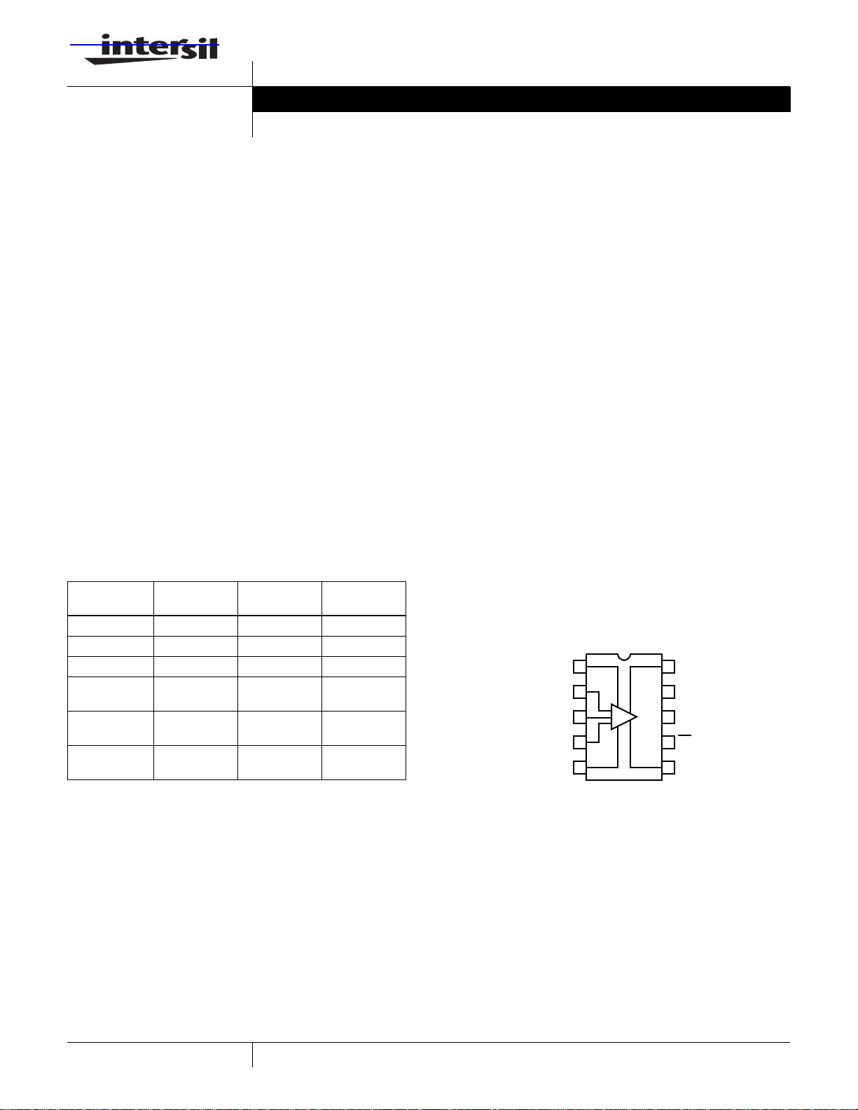
Pinout
EL5176
(10-PIN MSOP)
TOP VIEW
1
FBP
IN+
2
REF
IN-
+
3
-
4
5 6FBN OUT-
10
9
8
7
OUT+
VS-
VS+
EN
1
CAUTION: These devices are sensitive to electrostatic discharge; follow proper IC Handling Procedures.
1-888-INTERSIL or 1-888-468-3774
| Intersil (and design) is a registered trademark of Intersil Americas Inc.
All other trademarks mentioned are the property of their respective owners.
Copyright Intersil Americas Inc. 2003-2005. All Rights Reserved
EL5176
Absolute Maximum Ratings (T
Supply Voltage (V
Maximum Output Current. . . . . . . . . . . . . . . . . . . . . . . . . . . . ±60mA
+ to VS-) . . . . . . . . . . . . . . . . . . . . . . . . . . . .12V
S
= 25°C)
A
Operating Junction Temperature . . . . . . . . . . . . . . . . . . . . . . +135°C
Ambient Operating Temperature . . . . . . . . . . . . . . . .-40°C to +85°C
Storage Temperature Range . . . . . . . . . . . . . . . . . .-65°C to +150°C
CAUTION: Stresses above those listed in “Absolute Maximum Ratings” may cause permanent damage to the device. This is a stress only rating and operation of the
device at these or any other conditions above those indicated in the operational sections of this specification is not implied.
IMPORTANT NOTE: All parameters having Min/Max specifications are guaranteed. Typ values are for information purposes only. Unless otherwise noted, all tests are
at the specified temperature and are pulsed tests, therefore: T
Electrical Specifications V
+ = +5V, VS- = -5V, TA = 25°C, VIN = 0V, RLD = 1kΩ, RF = 0, RG = OPEN, CLD = 2.7pF, Unless Otherwise
S
= TC = T
J
A
Specified
PARAMETER DESCRIPTION CONDITIONS MIN TYP MAX UNIT
AC PERFORMANCE
BW -3dB Bandwidth A
BW ±0.1dB Bandwidth A
SR Slew Rate - Rise V
Slew Rate - Fall V
T
T
STL
OVR
Settling Time to 0.1% V
Output Overdrive Recovery Time 20 ns
= 1, CLD = 2.7pF 250 MHz
V
A
= 2, RF = 500, CLD = 2.7pF 60 MHz
V
= 10, RF = 500, CLD = 2.7pF 10 MHz
A
V
= 1, CLD = 2.7pF 50 MHz
V
OUT
OUT
OUT
= 3V
= 3V
= 2V
, 20% to 80% 600 800 1000 V/µs
P-P
, 20% to 80% 540 700 1000 V/µs
P-P
P-P
10 ns
GBWP Gain Bandwidth Product 100 MHz
BW (-3dB) V
V
REF
V
SR+ V
REF
V
SR- V
REF
V
N
I
N
HD2 Second Harmonic Distortion V
HD3 Third Harmonic Distortion V
dG Differential Gain at 3.58MHz R
dθ Differential Phase at 3.58MHz R
-3dB Bandwidth AV =1, CLD = 2.7pF 50 MHz
REF
Slew Rate - Rise V
REF
Slew Rate - Fall V
REF
OUT
OUT
= 2V
= 2V
, 20% to 80% 90 V/µs
P-P
, 20% to 80% 50 V/µs
P-P
Input Voltage Noise at 10kHz 26 nV/√Hz
Input Current Noise at 10kHz 2 pA/√Hz
OUT
V
OUT
OUT
V
OUT
= 300Ω, A
L
= 300Ω, A
L
= 2V
= 2V
= 2V
= 2V
, 5MHz -94 dBc
P-P
, 20MHz -94 dBc
P-P
, 5MHz -77 dBc
P-P
, 20MHz -75 dBc
P-P
= 2 0.1 %
V
= 2 0.5 °
V
INPUT CHARACTERISTICS
V
I
IN
I
REF
R
C
OS
IN
IN
Input Referred Offset Voltage ±1.5 ±25 mV
Input Bias Current (VIN+, VIN-) -14 -6 -3 µA
Input Bias Current (V
)0.51.34µA
REF
Differential Input Resistance 300 kΩ
Differential Input Capacitance 1pF
DMIR Differential Mode Input Range ±2.1 ±2.3 ±2.5 V
CMIR+ Common Mode Positive Input Range at V
CMIR- Common Mode Negative Input Range at V
V
+ Positive Reference Input Voltage Range VIN+ = VIN- = 0V 3.5 3.8 V
REFIN
V
- Negative Reference Input Voltage Range VIN+ = VIN- = 0V -3.3 -3 V
REFIN
V
REFOS
Output Offset Relative to V
±60 ±100 mV
REF
+, VIN-3.13.4V
IN
+, VIN- -4.5 -4.2 V
IN
2
FN7343.2
August 3, 2005
EL5176
Electrical Specifications V
+ = +5V, VS- = -5V, TA = 25°C, VIN = 0V, RLD = 1kΩ, RF = 0, RG = OPEN, CLD = 2.7pF, Unless Otherwise
S
Specified (Continued)
PARAMETER DESCRIPTION CONDITIONS MIN TYP MAX UNIT
CMRR Input Common Mode Rejection Ratio V
Gain Gain Accuracy V
= ±2.5V 65 82 dB
IN
= 1 0.981 0.996 1.011 V
IN
OUTPUT CHARACTERISTICS
V
OUT
Positive Output Swing RL = 500Ω to GND 3.6 3.9 V
Negative Output Swing -3.8 -3.5 V
I
(Max) Maximum Source Output Current RL = 10Ω,
OUT
Maximum Sink Output Current -40 -30 mA
R
OUT
Output Impedance 130 mΩ
V
+ = 1.1V,
IN
V
- = -1.1V,
IN
V
REF
= 0
35 50 mA
SUPPLY
V
SUPPLY
I
S(ON)
I
+ Positive Power Supply Current - Disabled EN pin tied to 4.8V 80 120 µA
S(OFF)
I
- Negative Power Supply Current - Disabled -200 -120 µA
S(OFF)
PSRR Power Supply Rejection Ratio V
Supply Operating Range VS+ to VS-4.7511V
Power Supply Current - Per Channel 6.8 7.5 8.2 mA
from ±4.5V to ±5.5V 70 84 dB
S
ENABLE
t
EN
t
DS
V
IH
V
IL
Enable Time 215 ns
Disable Time 0.95 µs
EN Pin Voltage for Power-Up VS+ -
1.5
EN Pin Voltage for Shut-Down VS+ -
0.5
I
IH-EN
I
IL-EN
EN Pin Input Current High At VEN = 5V 40 60 µA
EN Pin Input Current Low At VEN = 0V -6 -2.5 µA
V
V
Pin Descriptions
PIN NUMBER PIN NAME PIN DESCRIPTION
1 FBP Non-inverting feedback input; resistor R
2 IN+ Non-inverting input
3 REF Output common-mode control; the common-mode voltage of V
4 IN- Inverting input
5 FBN Inverting feedback input; resistor R
6 OUT- Inverting output
7EN
Enabled when this pin is floating or the applied voltage ≤ VS+ -1.5
8 VS+ Positive supply
9 VS- Negative supply
10 OUT+ Non-inverting output
3
must be connected from this pin to V
F1
must be connected from this pin to V
F2
OUT
will follow the voltage on this pin
OUT
OUT
FN7343.2
August 3, 2005
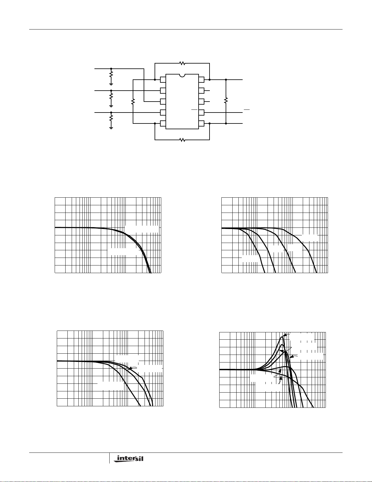
Connection Diagram
VREF
R
50Ω
EL5176
R
F1
0Ω
S3
1
FBP
OUT+
10
OUT+
INP
R
INN-
50Ω
R
50Ω
S1
S2
R
OPEN
Typical Performance Curves
AV = 1, RLD = 1kΩ, CLD = 2.7pF
4
3
2
1
0
-1
-2
-3
MAGNITUDE (dB)
-4
-5
-6
1M
10M 100M 1G
FREQUENCY (Hz)
V
OP-P
= 1V
G
V
OP-P
P-P
= 200mV
IN+
2
REF
3
IN-
4
5 6FBN OUT-
VS-
VS+
EN
R
F2
0Ω
9
-5V
R
8
+5V
7
NORMALIZED MAGNITUDE (dB)
LD
1kΩ
R
= 1kΩ, CLD = 2.7pF
LD
4
3
2
1
0
-1
-2
-3
-4
-5
-6
1M
EN
OUT-
AV = 1
AV = 5
AV = 10
10M 100M 1G
FREQUENCY (Hz)
AV = 2
FIGURE 1. FREQUENCY RESPONSE FIGURE 2. FREQUENCY RESPONSE FOR VARIOUS GAIN
A
= 1, CLD = 2.7pF
V
4
3
2
1
0
-1
-2
-3
-4
NORMINALIZED GAIN (dB)
-5
-6
1M
10M 100M 1G
FREQUENCY (Hz)
RLD = 1kΩ
RLD = 200Ω
FIGURE 3. FREQUENCY RESPONSE vs R
RLD = 500Ω
LD
AV = 1, RLD = 1kΩ
5
4
3
2
1
0
-1
-2
MAGNITUDE (dB)
-3
-4
-5
1M
C
= 9pF
LD
C
= 2.7pF
LD
10M 100M 1G
FREQUENCY (Hz)
FIGURE 4. FREQUENCY RESPONSE vs C
C
= 56pF
LD
C
= 34pF
LD
C
LD
4
= 23pF
LD
August 3, 2005
FN7343.2

Typical Performance Curves (Continued)
A
= 2, RLD = 1kΩ, CLD = 2.7pF
V
10
9
8
7
6
5
4
3
2
NORMALIZED GAIN (dB)
1
0
1M
RF = 200Ω
10M 100M 400M
FREQUENCY (Hz)
RF = 1kΩ
RF = 500Ω
EL5176
= 2, RF = 1kΩ, CLD = 2.7pF
A
V
10
9
8
7
6
5
4
3
2
NORMALIZED GAIN (dB)
1
0
1M
R
= 1kΩ
LD
RLD = 500Ω
R
= 200Ω
LD
10M 100M 400M
FREQUENCY (Hz)
FIGURE 5. FREQUENCY RESPONSE FIGURE 6. FREQUENCY RESPONSE vs R
5
4
3
2
1
0
-1
-2
MAGNITUDE (dB)
-3
-4
-5
100K
1M 10M 100M
FREQUENCY (Hz)
FIGURE 7. FREQUENCY RESPONSE - V
0
-10
-20
-30
-40
-50
PSRR (dB)
-60
-70
-80
-90
1K
10K 1M 100M
PSRR-
PSRR+
100K
FREQUENCY (Hz)
FIGURE 9. PSRR vs FREQUENCY
10M
REF
100
10
1
IMPEDENCE (Ω)
0.1
10K
100K 1M 100M
FREQUENCY (Hz)
10M
FIGURE 8. OUTPUT IMPEDANCE vs FREQUENCY
100
90
80
70
60
50
40
CMRR (dB)
30
20
10
0
100K
1M 100M
10M
FREQUENCY (Hz)
FIGURE 10. CMRR vs FREQUENCY
LD
1G
5
FN7343.2
August 3, 2005

Typical Performance Curves (Continued)
1K
100
E
N
10
VOLTAGE NOISE (nV/√Hz),
CURRENT NOISE (pA/√Hz)
1
100 100K 10M
10
10K
1K
FREQUENCY (Hz)
FIGURE 11. VOLTAGE AND CURRENT NOISE vs FREQUENCY
= ±5V, AV = 1, RLD = 1kΩ
V
S
-50
-55
-60
-65
-70
-75
-80
DISTORTION (dB)
-85
-90
-95
123456789
D
H
f
(
2
D
H
2
D
H
HD3 (f = 5MHz)
M
0
2
=
f
(
3
)
z
H
M
5
=
H
M
0
2
=
f
(
V
OP-P, DM
FIGURE 13. HARMONIC DISTORTION vs DIFFERENTIAL
OUTPUT VOLTAGE
I
N
1M
)
z
H
)
z
10
(V)
EL5176
VS = ±5V, AV = 1, RLD = 1kΩ
-50
-55
-60
-65
-70
-75
-80
-85
DISTORTION (dB)
-90
-95
-100
1 1.5 2 2.5 3 3.5 4 4.5 5
H
D
3
D
H
(
f
=
2
=
f
(
3
2
D
H
V
OP-P, DM
0
M
H
z
)
)
z
H
M
5
)
z
H
M
0
2
=
f
(
D2
H
(V)
)
z
H
M
5
=
f
(
FIGURE 12. HARMONIC DISTORTION vs DIFFERENTIAL
OUTPUT VOLTAGE
V
= ±5V, AV = 1, V
S
-50
-55
-60
H
D
-65
-70
-75
-80
-85
DISTORTION (dB)
-90
-95
-100
100 800400 900
H
D
3
3
(
f
=
H
D
H
D
2
200 600
(
f
2
0
2
(
(
=
M
H
z
)
f
=
2
0
M
H
z
)
f
=
5
M
H
z
)
300 500 700
FIGURE 14. HARMONIC DISTORTION vs R
OP-P, DM
5
M
H
z
)
R
LD
= 1V
1000
(Ω)
LD
= ±5V, AV = 2, V
V
S
-40
-50
-60
-70
-80
DISTORTION (dB)
-90
-100
HD3 (f = 5MHz)
H
D
2
(
f
=
2
0
M
H
z
)
HD2 (f = 5MHz)
400 600 800
300 700
200 900500 1000
OP-P, DM
HD3 (f = 20MHz)
R
LD
= 2V
(Ω)
FIGURE 15. HARMONIC DISTORTION vs R
6
LD
VS = ±5V, RLD = 1kΩ, V
V
OP-P, DM
-40
-50
-60
-70
-80
DISTORTION (dB)
-90
-100
= 2V for AV = 2
=
V
A
(
3
D
H
20 30 40 50 60
100
FREQUENCY (MHz)
OP-P, DM
HD3 (AV = 1)
)
2
= 1V for AV = 1,
A
(
2
D
H
A
(
2
D
H
)
2
=
V
)
1
=
V
FIGURE 16. HARMONIC DISTORTION vs FREQUENCY
FN7343.2
August 3, 2005

Typical Performance Curves (Continued)
EL5176
50mV/DIV
10ns/DIV
FIGURE 17. SMALL SIGNAL TRANSIENT RESPONSE
M = 100ns, CH1 = 500mV/DIV, CH2 = 5V/DIV
CH1
CH2
100ns/DIV
FIGURE 19. ENABLED RESPONSE
0.5V/DIV
10ns/DIV
FIGURE 18. LARGE SIGNAL TRANSIENT RESPONSE
M = 200ns, CH1 = 500mV/DIV, CH2 = 5V/DIV
CH1
CH2
200ns/DIV
FIGURE 20. DISABLED RESPONSE
JEDEC JESD51-3 LOW EFFECTIVE THERMAL
CONDUCTIVITY TEST BOARD
0.6
0.5
486mW
0.4
0.3
0.2
POWER DISSIPATION (W)
0.1
0
0 25 50 75 100 125
AMBIENT TEMPERATURE (°C)
MSOP8/10
θJA=206°C/W
85
FIGURE 21. PACKAGE POWER DISSIPATION vs AMBIENT
TEMPERATURE
7
JEDEC JESD51-7 HIGH EFFECTIVE THERMAL
CONDUCTIVITY TEST BOARD
1
0.9
870mW
0.8
0.7
0.6
0.5
0.4
0.3
0.2
POWER DISSIPATION (W)
0.1
0
0 25 50 75 100 125
AMBIENT TEMPERATURE (°C)
MSOP8/10
θJA=115°C/W
85
FIGURE 22. PACKAGE POWER DISSIPATION vs AMBIENT
TEMPERATURE
FN7343.2
August 3, 2005

Simplified Schematic
EL5176
VS+
R
R
1
R
2
FBNFBPIN-IN+
3
R
C
C
R
5
Description of Operation and Application
Information
Product Description
The EL5176 is a wide bandwidth, low power and
single/differential ended to differential output amplifier. It can
be used as single/differential ended to differential converter.
The EL5176 is internally compensated for closed loop gain
of +1 of greater. Connected in gain of 1 and driving a 1kΩ
differential load, the EL5176 has a -3dB bandwidth of
250MHz. Driving a 200Ω differential load at gain of 2, the
bandwidth is about 30MHz. The EL5176 is available with a
power down feature to reduce the power while the amplifier
is disabled.
R
4
R
7
8
V
B1
V
B2
C
C
R
6
V
-
S
OUT+
OUT-
R
CD
R
CD
R
REF
R
10
9
The gain setting for EL5176 is:
R
V
ODMVIN
V
ODM
=
V
OCMVREF
+1
×=
VIN( +VIN-) 1
+
F1RF2
----------------------------+
R
G
2R
F
-----------+
×–=
R
G
Where:
•R
= RF2 = R
F1
F
R
F1
Input, Output, and Supply Voltage Range
The EL5176 has been designed to operate with a single
supply voltage of 5V to 10V or a split supplies with its total
voltage from 5V to 10V. The amplifier has an input common
mode voltage range from -4.5V to 3.4V for ±5V supply. The
differential mode input range (DMIR) between the two inputs
is from -2.3V to +2.3V. The input voltage range at the REF
pin is from -3.3V to 3.8V. If the input common mode or
differential mode signal is outside the above-specified
ranges, it will cause the output signal distorted.
The output of the EL5176 can swing from -3.8V to +3.9V at
1kΩ differential load at ±5V supply. As the load resistance
becomes lower, the output swing is reduced.
Differential and Common Mode Gain Settings
The voltage applied at REF pin can set the output common
mode voltage and the gain is one. The differential gain is set
by the R
and RG network.
F
8
FBP
VIN+
V
V
REF
R
-
IN
IN+
G
IN-
REF
FBN
R
F2
VO+
VO-
FIGURE 23.
Choice of Feedback Resistor and Gain Bandwidth
Product
For applications that require a gain of +1, no feedback
resistor is required. Just short the OUT+ pin to FBP pin and
OUT- pin to FBN pin. For gains greater than +1, the
feedback resistor forms a pole with the parasitic capacitance
at the inverting input. As this pole becomes smaller, the
amplifier's phase margin is reduced. This causes ringing in
the time domain and peaking in the frequency domain.
Therefore, R
exceeded for optimum performance. If a large value of R
must be used, a small capacitor in the few Pico farad range
has some maximum value that should not be
F
FN7343.2
August 3, 2005
F

EL5176
in parallel with RF can help to reduce the ringing and
peaking at the expense of reducing the bandwidth.
The bandwidth of the EL5176 depends on the load and the
feedback network. R
and RG appear in parallel with the
F
load for gains other than +1. As this combination gets
smaller, the bandwidth falls off. Consequently, R
also has a
F
minimum value that should not be exceeded for optimum
bandwidth performance. For gain of +1, R
= 0 is optimum.
F
For the gains other than +1, optimum response is obtained
with R
between 500Ω to 1kΩ.
F
The EL5176 has a gain bandwidth product of 100MHz for
R
= 1kΩ. For gains ≥5, its bandwidth can be predicted by
LD
the following equation:
Gain BW 100MHz=×
Driving Capacitive Loads and Cables
The EL5176 can drive 50pF differential capacitor in parallel
with 1kΩ differential load with less than 5dB of peaking at
gain of +1. If less peaking is desired in applications, a small
series resistor (usually between 5Ω to 50Ω) can be placed in
series with each output to eliminate most peaking. However,
this will reduce the gain slightly. If the gain setting is greater
than 1, the gain resistor R
for any gain loss which may be created by the additional
series resistor at the output.
When used as a cable driver, double termination is always
recommended for reflection-free performance. For those
applications, a back-termination series resistor at the
amplifier's output will isolate the amplifier from the cable and
allow extensive capacitive drive. However, other applications
may have high capacitive loads without a back-termination
resistor. Again, a small series resistor at the output can help
to reduce peaking.
can then be chosen to make up
G
±40mA. This limit is set by the design of the internal metal
interconnect.
Power Dissipation
With the high output drive capability of the EL5176. It is
possible to exceed the 135°C absolute maximum junction
temperature under certain load current conditions.
Therefore, it is important to calculate the maximum junction
temperature for the application to determine if the load
conditions or package types need to be modified for the
amplifier to remain in the safe operating area.
The maximum power dissipation allowed in a package is
determined according to:
T
–
PD
MAX
Where:
•T
JMAX
•T
AMAX
• θ
JA
The maximum power dissipation actually produced by an IC
is the total quiescent supply current times the total power
supply voltage, plus the power in the IC due to the load, or:
PD V
Where:
•V
S
•I
SMAX
• ∆V
application
JMAXTAMAX
-------------------------------------------- -=
Θ
JA
= Maximum junction temperature
= Maximum ambient temperature
= Thermal resistance of the package
∆V
O
SISMAXVS
------------×+×=
R
LD
= Total supply voltage
= Maximum quiescent supply current per channel
= Maximum differential output voltage of the
O
Disable/Power-Down
The EL5176 can be disabled and placed its outputs in a high
impedance state. The turn off time is about 0.95µs and the
turn on time is about 215ns. When disabled, the amplifier's
supply current is reduced to 1.7µA for I
+ and 120µA for IS-
S
typically, thereby effectively eliminating the power
consumption. The amplifier's power down can be controlled
by standard CMOS signal levels at the ENABLE pin. The
applied logic signal is relative to V
float or applying a signal that is less than 1.5V below V
+ pin. Letting the EN pin
S
+ will
S
enable the amplifier. The amplifier will be disabled when the
signal at EN
pin is above VS+ - 0.5V.
Output Drive Capability
The EL5176 has internal short circuit protection. Its typical
short circuit current is ±40mA for EL5176. If the output is
shorted indefinitely, the power dissipation could easily
increase such that the part will be destroyed. Maximum
reliability is maintained if the output current never exceeds
9
•R
= Differential load resistance
LD
•I
By setting the two PD
can solve the output current and R
= Load current
LOAD
equations equal to each other, we
MAX
to avoid the device
LD
overheat.
Power Supply Bypassing and Printed Circuit
Board Layout
As with any high frequency device, a good printed circuit
board layout is necessary for optimum performance. Lead
lengths should be as sort as possible. The power supply pin
must be well bypassed to reduce the risk of oscillation. For
normal single supply operation, where the V
connected to the ground plane, a single 4.7µF tantalum
capacitor in parallel with a 0.1µF ceramic capacitor from V
to GND will suffice. This same capacitor combination should
be placed at each supply pin to ground if split supplies are to
be used. In this case, the V
- pin becomes the negative
S
supply rail.
- pin is
S
S
FN7343.2
August 3, 2005
+

EL5176
For good AC performance, parasitic capacitance should be
kept to minimum. Use of wire wound resistors should be
avoided because of their additional series inductance. Use
of sockets should also be avoided if possible. Sockets add
parasitic inductance and capacitance that can result in
Typical Applications
R
F
FBP
R
R
G
T
IN+
IN-
REF
FBN
EL5176
R
F
FIGURE 24. TWISTED PAIR CABLE RECEIVER
As the signal is transmitted through a cable, the high
frequency signal will be attenuated. One way to compensate
this loss is to boost the high frequency gain at the receiver
side.
R
F
50
50
compromised performance. Minimizing parasitic capacitance
at the amplifier's inverting input pin is very important. The
feedback resistor should be placed very close to the
inverting input pin. Strip line design techniques are
recommended for the signal traces.
TWISTED PAIR
= 100Ω
Z
O
R
GR
Gain
(dB)
IN+
IN-
REF
EL5172
R
FR
V
O
R
T
R
GC
75
C
L
DC Gain 1
HF()Gain 1
R
G
2R
-----------+=
R
--------------------------+=
RGR
FBP
IN+
I
-
N
REF
FBN
R
F
F
G
2R
F
||
GC
VO+
VO-
f
L
1
f
------------------------ -≅
L
2π R
GCC
---------------------------- -≅
2π R
1
GCCC
f
H
f
H
frequency
FIGURE 25. TRANSMIT EQUALIZER
10
FN7343.2
August 3, 2005

MSOP Package Outline Drawing
EL5176
NOTE: The package drawing shown here may not be the latest version. To check the latest revision, please refer to the Intersil website at
http://www.intersil.com/design/packages/index.asp
All Intersil U.S. products are manufactured, assembled and tested utilizing ISO9000 quality systems.
Intersil Corporation’s quality certifications can be viewed at www.intersil.com/design/quality
Intersil products are sold by description only. Intersil Corporation reserves the right to make changes in circuit design, software and/or specifications at any time without
notice. Accordingly, the reader is cautioned to verify that data sheets are current before placing orders. Information furnished by Intersil is believed to be accurate and
reliable. However, no responsibility is assumed by Intersil or its subsidiaries for its use; nor for any infringements of patents or other rights of third parties which may result
from its use. No license is granted by implication or otherwise under any patent or patent rights of Intersil or its subsidiaries.
For information regarding Intersil Corporation and its products, see www.intersil.com
11
FN7343.2
August 3, 2005
 Loading...