


查询EL5144供应商
®
EL5144, EL5146, EL5244, EL5246, EL5444
Data Sheet April 13, 2005
100MHz Single-Supply Rail-to-Rail
Amplifiers
The EL5144 series amplifiers are voltage-feedback, high
speed, rail-to-rail amplifiers designed to operate on a single
+5V supply. They offer unity gain stability with an unloaded 3dB bandwidth of 100MHz. The input common-mode voltage
range extends from the negative rail to within 1.5V of the
positive rail. Driving a 75Ω double terminated coaxial cable,
the EL5144 series amplifiers drive to within 150mV of either
rail. The 200V/µs slew rate and 0.1%/0.1° differential
gain/differential phase makes these parts ideal for composite
and component video applications. With their voltagefeedback architecture, these amplifiers can accept reactive
feedback networks, allowing them to be used in analog
filtering applications These amplifiers will source 90mA and
sink 65mA.
The EL5146 and EL5246 have a power-savings disable
feature. Applying a standard TTL low logic level to the CE
(Chip Enable) pin reduces the supply current to 2.6µA within
10ns. Turn-on time is 500ns, allowing true break-beforemake conditions for multiplexing applications. Allowing the
CE pin to float or applying a high logic level will enable the
amplifier.
For applications where board space is critical, singles are
offered in a 5-pin SOT-23 package, duals in 8- and 10-pin
MSOP packages, and quads in a 16-pin QSOP package.
Singles, duals, and quads are also available in industrystandard pinouts in SO and PDIP packages. All parts
operate over the industrial temperature range of -40°C to
+85°C.
FN7177.1
Features
• Rail-to-rail output swing
• -3dB bandwidth = 100MHz
• Single-supply +5V operation
• Power-down to 2.6µA
• Large input common-mode range 0V < VCM < 3.5V
• Diff gain/phase = 0.1%/0.1°
• Low power 35mW per amplifier
• Space-saving SOT23-5, MSOP8 & 10, & QSOP16
packages
• Pb-Free available (RoHS compliant)
Applications
• Video amplifiers
• 5V analog signal processing
• Multiplexers
• Line drivers
• Portable computers
• High speed communications
• Sample & hold amplifiers
• Comparators
1
CAUTION: These devices are sensitive to electrostatic discharge; follow proper IC Handling Procedures.
1-888-INTERSIL or 1-888-352-6832
| Intersil (and design) is a registered trademark of Intersil Americas Inc.
Copyright Intersil Americas Inc. 2003, 2005. All Rights Reserved
All other trademarks mentioned are the property of their respective owners.

EL5144, EL5146, EL5244, EL5246, EL5444
Ordering Information
PART NUMBER PACKAGE TAPE & REEL PKG. DWG. #
EL5144CW-T7 5-Pin SOT-23* 7” (3K pcs) MDP0038
EL5144CW-T7A 5-Pin SOT-23* 7” (250 pcs) MDP0038
EL5144CWZ-T7
(See Note)
EL5144CWZ-T7A
(See Note)
EL5146CN 8-Pin PDIP - MDP0031
EL5146CS 8-Pin SOIC - MDP0027
EL5146CS-T7 8-Pin SOIC 7” MDP0027
EL5146CS-T13 8-Pin SOIC 13” MDP0027
EL5146CSZ
(See Note)
EL5146CSZ-T7
(See Note)
EL5146CSZ-T13
(See Note)
EL5244CN 8-Pin PDIP - MDP0031
EL5244CS 8-Pin SOIC - MDP0027
EL5244CS-T7 8-Pin SOIC 7” MDP0027
EL5244CS-T13 8-Pin SOIC 13” MDP0027
EL5244CSZ
(See Note)
EL5244CSZ-T7
(See Note)
EL5244CSZ-T13
(See Note)
EL5244CY 8-Pin MSOP - MDP0043
EL5244CY-T13 8-Pin MSOP 13” MDP0043
EL5244CYZ
(See Note)
EL5244CYZ-T7
(See Note)
EL5244CYZ-T13
(See Note)
EL5246CN 14-Pin PDIP - MDP0031
EL5246CS 14-Pin SOIC - MDP0027
EL5246CS-T7 14-Pin SOIC 7” MDP0027
EL5246CS-T13 14-Pin SOIC 13” MDP0027
EL5246CSZ
(See Note)
EL5246CSZ-T7
(See Note)
EL5246CSZ-T13
(See Note)
EL5246CY 10-Pin MSOP - MDP0043
EL5246CY-T13 10-Pin MSOP 13” MDP0043
5-Pin SOT-23*
(Pb-free)
5-Pin SOT-23*
(Pb-free)
8-Pin SOIC
(Pb-free)
8-Pin SOIC
(Pb-free)
8-Pin SOIC
(Pb-free)
8-Pin SOIC
(Pb-free)
8-Pin SOIC
(Pb-free)
8-Pin SOIC
(Pb-free)
8-Pin MSOP
(Pb-free)
8-Pin MSOP
(Pb-free)
8-Pin MSOP
(Pb-free)
14-Pin SOIC
(Pb-free)
14-Pin SOIC
(Pb-free)
14-Pin SOIC
(Pb-free)
7” (3K pcs) MDP0038
7” (250 pcs) MDP0038
- MDP0027
7” MDP0027
13” MDP0027
- MDP0027
7” MDP0027
13” MDP0027
- MDP0043
7” MDP0043
13” MDP0043
- MDP0027
7” MDP0027
13” MDP0027
Ordering Information (Continued)
PART NUMBER PACKAGE TAPE & REEL PKG. DWG. #
EL5246CYZ
(See Note)
EL5246CYZ-T7
(See Note)
EL5246CYZ-T13
(See Note)
EL5444CN 14-Pin PDIP - MDP0031
EL5444CS 14-Pin SOIC - MDP0027
EL5444CS-T7 14-Pin SOIC 7” MDP0027
EL5444CS-T13 14-Pin SOIC 13” MDP0027
EL5444CSZ
(See Note)
EL5444CSZ-T7
(See Note)
EL5444CSZ-T13
(See Note)
EL5444CU 16-Pin QSOP - MDP0040
EL5444CU-T13 16-Pin QSOP 13” MDP0040
EL5444CUZ
(See Note)
EL5444CUZ-T7
(See Note)
EL5444CUZ-T13
(See Note)
*EL5144CW symbol is .Jxxx where xxx represents date
NOTE: Intersil Pb-free products employ special Pb-free material
sets; molding compounds/die attach materials and 100% matte tin
plate termination finish, which are RoHS compliant and compatible
with both SnPb and Pb-free soldering operations. Intersil Pb-free
products are MSL classified at Pb-free peak reflow temperatures that
meet or exceed the Pb-free requirements of IPC/JEDEC J STD-020.
10-Pin MSOP
(Pb-free)
10-Pin MSOP
(Pb-free)
10-Pin MSOP
(Pb-free)
14-Pin SOIC
(Pb-free)
14-Pin SOIC
(Pb-free)
14-Pin SOIC
(Pb-free)
16-Pin QSOP
(Pb-free)
16-Pin QSOP
(Pb-free)
16-Pin QSOP
(Pb-free)
- MDP0043
7” MDP0043
13” MDP0043
- MDP0027
7” MDP0027
13” MDP0027
- MDP0040
7” MDP0040
13” MDP0040
2

s
Pinouts
EL5144
(5-PIN SOT-23)
TOP VIEW
EL5144, EL5146, EL5244, EL5246, EL5444
EL5146 & EL5146
(8-PIN SO, PDIP)
TOP VIEW
1
OUT
2
GND
IN+
3
-+
EL5244
(8-PIN SOIC, PDIP, MSOP)
TOP VIEW
1
OUT
A
INA-
2
-
+
INA+
3
4
GND
EL5444
(14-PIN SOIC, PDIP)
TOP VIEW
5
VS
4
IN-
EL5246
(10-PIN MSOP)
TOP VIEW
V
8
S
7
OUT
B
INB-
6
-
+
+
IN
5
B
INA+
CEA
GND
CEB
INB+
1
2
3
4
-
+
+
-
INA-
10
OUT
9
A
8
V
S
7
OUT
B
65
INB-
1
NC
2
IN-
3
IN+
4
GND
(14-PIN SOIC, PDIP)
TOP VIEW
1
INA+
2
NC
3
CEA
4
GND
CEB
5
NC
6
7
INB+
-
+
EL5246
-
+
+
-
8
CE
7
VS
6
OUT
5
NC
14
INA-
13
OUT
A
12
NC
11
V
S
10
NC
9
OUT
B
8
INB-
EL5444
(16-PIN QSOP)
TOP VIEW
OUT
INA+
INB+
OUT
INA-
IN
1
A
2
-
+
3
4
V
S
5
+
-
-
6
B
7
B
14
OUT
D
+
-
13
IND-
12
IND+
11
GND
10
INC+
-
+
9
INC-
8
OUT
C
1
OUT
A
2
IN
INA+
INB+
OUT
-
A
V
S
V
S
-
IN
B
B
-
3
4
5
6
-
7
8 9
+
+
16
OUT
D
+
-
15
IN
-
D
14
IND+
13
GND
12
GND
11
INC+
-
+
10
INC-
OUT
C
3

EL5144, EL5146, EL5244, EL5246, EL5444
Absolute Maximum Ratings (T
Supply Voltage between V
Maximum Continuous Output Current . . . . . . . . . . . . . . . . . . . 50mA
Power Dissipation . . . . . . . . . . . . . . . . . . . . . . . . . . . . . See Curves
CAUTION: Stresses above those listed in “Absolute Maximum Ratings” may cause permanent damage to the device. This is a stress only rating and operation of the
device at these or any other conditions above those indicated in the operational sections of this specification is not implied .
IMPORTANT NOTE: All parameters having Min/Max specifications are guaranteed. Typical values are for information purposes only. Unless otherwise noted, all tests
are at the specified temperature and are pulsed tests , therefore: T
and GND. . . . . . . . . . . . . . . . . . . . .+6V
S
Electrical Specifications V
= 25°C)
A
Pin Voltages. . . . . . . . . . . . . . . . . . . . . . . . . GND -0.5V to V
Storage Temperature. . . . . . . . . . . . . . . . . . . . . . . .- 65°C to +150°C
Operating Temperature . . . . . . . . . . . . . . . . . . . . . . .-40°C to +85°C
= TC = T
J
= +5V, GND = 0V, TA = 25°C, CE = +2V, unless otherwise specified.
S
A
+0.5V
S
PARAMETER DESCRIPTION CONDITIONS MIN TYP MAX UNIT
AC PERFORMANCE
d
G
d
P
BW Bandwidth -3dB, G = 1, R
BW1 Bandwidth ±0.1dB, G = 1, R
Differential Gain Error (Note 1) G = 2, RL = 150Ω to 2.5V, RF = 1kΩ 0.1 %
Differential Phase Error (Note 1) G = 2, RL = 150Ω to 2.5V, RF = 1kΩ 0.1 °
= 10kΩ, RF = 0 100 MHz
L
-3dB, G = 1, R
= 150Ω, RF = 0 60 MHz
L
= 150Ω to GND, RF = 0 8 MHz
L
GBWP Gain Bandwidth Product 60 MHz
SR Slew Rate G = 1, R
to 3.5V
t
S
Settling Time to 0.1%, V
= 150Ω to GND, RF = 0, VO = 0.5V
L
= 0V to 3V 35 ns
OUT
150 200 V/µs
DC PERFORMANCE
A
VOL
V
OS
T
CVOS
I
B
Open Loop Voltage Gain RL = no load, V
= 150Ω to GND, V
R
L
Offset Voltage V
= 1V, SOT23-5 and MSOP packages 25 mV
CM
V
= 1V, All other packages 15 mV
CM
Input Offset Voltage Temperature
Coefficient
Input Bias Current V
= 0V & 3.5V 2 100 nA
CM
= 0.5V to 3V 54 65 dB
OUT
= 0.5V to 3V 40 50 dB
OUT
10 mV/°C
INPUT CHARACTERISTICS
CMIR Common Mode Input Range CMRR
CMRR Common Mode Rejection Ratio DC, V
R
IN
C
IN
Input Resistance 1.5 GΩ
Input Capacitance 1.5 pF
≥ 47dB 0 3.5 V
= 0 to 3.0V 50 60 dB
CM
DC, V
= 0 to 3.5V 47 60 dB
CM
OUTPUT CHARACTERISTICS
V
V
+I
-I
OP
ON
OUT
OUT
Positive Output Voltage Swing RL = 150Ω to 2.5V (Note 2) 4.70 4.85 V
= 150Ω to GND (Note 2) 4.20 4.65 V
R
L
R
= 1kΩ to 2.5V (Note 2) 4.95 4.97 V
L
Negative Output Voltage Swing RL = 150Ω to 2.5V (Note 2) 0.15 0.30 V
= 150Ω to GND (Note 2) 0 V
R
L
= 1kΩ to 2.5V (Note 2) 0.03 0.05 V
R
L
Positive Output Current RL = 10Ω to 2.5V 60 90 120 mA
Negative Output Current RL = 10Ω to 2.5V -50 -65 -80 mA
ENABLE (EL5146 & EL5246 ONLY)
4

EL5144, EL5146, EL5244, EL5246, EL5444
Electrical Specifications V
= +5V, GND = 0V, TA = 25°C, CE = +2V, unless otherwise specified. (Continued)
S
PARAMETER DESCRIPTION CONDITIONS MIN TYP MAX UNIT
t
EN
t
DIS
I
IHCE
I
ILCE
V
IHCE
V
ILCE
Enable Time EL5146, EL5246 500 ns
Disable Time EL5146, EL5246 10 ns
CE pin Input High Current CE = 5V, EL5146, EL5246 0.003 1 mA
CE pin Input Low Current CE = 0V, EL5146, EL5246 -1.2 -3 mA
CE pin Input High Voltage for Power UpEL5146, EL5246 2.0 V
CE pin Input Low Voltage for Power
EL5146, EL5246 0.8 V
Down
SUPPLY
Is
Is
ON
OFF
Supply Current - Enabled (per
amplifier)
Supply Current - Disabled (per
amplifier)
No load, V
No load, V
= 0V, CE = 5V 7 8.8 mA
IN
= 0V, CE = 0V 2.6 5 mA
IN
PSOR Power Supply Operating Range 4.75 5.0 5.25 V
PSRR Power Supply Rejection Ratio DC, V
= 4.75V to 5.25V 50 60 dB
S
NOTES:
1. Standard NTSC test, AC signal amplitude = 286mV
is total load resistance due to feedback resistor and load resistor.
2. R
L
, f = 3.8MHz, V
P-P
is swept from 0.8V to 3.4V, RL is DC-coupled.
OUT
5

EL5144, EL5146, EL5244, EL5246, EL5444
Typical Performance Curves
Non-Inverting Frequency Response (Gain)
2
0
-2
AV=5.6, RF=1kΩ
-4
-6
Normalized Magnitude (dB)
VCM=1.5V
RL=150Ω
-8
1M 10M
Inverting Frequency Response (Gain) Inverting Frequency Response (Phase)
2
0
-2
-4
-6
VCM=1.5V
Normalized Magnitude (dB)
RF=1kΩ
RL=150Ω
-8
1M 10M
AV=1, RF=0Ω
AV=2, RF=1kΩ
100M 1M 10M
Frequency (Hz)
AV=-1
AV=-2
AV=-5.6
100M
Frequency (Hz)
Non-Inverting Frequency Response (Phase)
0
-45
AV=5.6, RF=1kΩ
-90
Phase (°)
-135
VCM=1.5V
-180
RL=150Ω
180
135
90
Phase (°)
45
VCM=1.5V
RF=1kΩ
0
RL=150Ω
1M 10M
AV=2, RF=1kΩ
AV=1, RF=0Ω
100M
Frequency (Hz)
AV=-1
AV=-2
AV=-5.6
100M
Frequency (Hz)
100
RL=150Ω
80
60
40
3dB Bandwidth (MHz)
20
0
-55 25
AV=1, RF=0Ω
AV=2, RF=1kΩ
AV=5.6, RF=1kΩ
Die Temperature (°C)
3dB Bandwidth vs Die Temperature for Various Gains 3dB Bandwidth vs Die Temperature for Various Gains
150
RL=10kΩ
120
90
60
3dB Bandwidth (MHz)
30
145-15 65 105
0
-55 25
Die Temperature (°C)
AV=1, RF=0Ω
AV=2, RF=1kΩ
AV=5.6, RF=1kΩ
145-15 65 105
6

EL5144, EL5146, EL5244, EL5246, EL5444
Typical Performance Curves (Continued)
Frequency Response for Various R
VCM=1.5V
4
RF=0Ω
=1
A
V
2
0
-2
Normalized Magnitude (dB)
-4
1M 10M
Frequency (Hz)
Frequency Response for Various RF and R
2
0
-2
-4
Normalized Magnitude (dB)
-6
1M 10M
VCM=1.5V
RL=150Ω
AV=2
RF=RG=1kΩ
RF=RG=560Ω
Frequency (Hz)
RL=10kΩ
RL=520Ω
RL=150Ω
L
G
RF=RG=2kΩ
100M
100M
Frequency Response for Various C
VCM=1.5V
8
RL=150Ω
=1
A
V
4
0
-4
Normalized Magnitude (dB)
-8
1M 10M
Group Delay vs Frequency
10
8
6
4
Group Delay (ns)
2
0
1M 10M
AV=2
RF=1kΩ
CL=47pF
CL=22pF
CL=0pF
Frequency (Hz)
AV=1
RF=1Ω
Frequency (Hz)
L
CL=100pF
100M
100M
Open Loop Gain and Phase vs Frequency Open Loop Voltage Gain vs Die Temperature
80
RL=1kΩ
60
RL=150Ω
40
Gain (dB)
20
0
1k 1M
Gain
Frequency (Hz)
Phase
0
45
Phase (°)
90
135
180
225
100M10k 10M100k
80
70
60
50
Open Loop Gain (dB)
40
30
-55 65
RL=150Ω
Die Temperature (°C)
No Load
145-15 10525
7

EL5144, EL5146, EL5244, EL5246, EL5444
Typical Performance Curves (Continued)
Voltage Noise vs Frequency - Video Amp
10k
1k
100
Voltage Noise (nV/√Hz)
10
10 100 10k 100M
Frequency (Hz)
(6 Typical Samples)
12
6
0
-6
Offset Voltage (mV)
-12
-55 65
Die Temperature (°C)
1M1k 100k 10M
Closed Loop Output Impedance vs Frequency
200
RF=0Ω
AV=2
)
20
O
2
Closed Loop (Z
0.2
10k 10M
Frequency (Hz)
PSRR and CMRR vs FrequencyOffset Voltage vs Die Temperature
20
0
-20
-40
PSRR, CMRR (dB)
-60
145-15 10525 1k 10M
-80
PSRR-
Frequency (Hz)
CMRR
PSRR+
100M100k 1M
100M100k 1M10k
Output Voltage Swing vs Frequency for THD < 1% Output Voltage Swing vs Frequency for THD < 0.1%
5
)
4
PP
3
RL=150Ω to 2.5V
2
1
Output Voltage Swing (V
0
1M 10M
RL=500Ω to 2.5V
Frequency (Hz)
RF=1kΩ
AV=2
100M
5
RF=1kΩ
AV=2
)
4
PP
3
2
1
Output Voltage Swing (V
0
1M 10M
RL=500Ω to 2.5V
RL=150Ω to 2.5V
Frequency (Hz)
100M
8

EL5144, EL5146, EL5244, EL5246, EL5444
Typical Performance Curves (Continued)
Large Signal Pulse Response (Single Supply) Small Signal Pulse Response (Single Supply)
4
3
VS=5V
RL=150Ω to 0V
RF=1kΩ
AV=2
1.9
1.7
VS=5V
RL=150Ω to 0V
RF=1kΩ
AV=2
2
Output Voltage (V)
1
0
Large Signal Pulse Response (Split Supplies)
4
2
0
Output Voltage (V)
-2
-4
Settling Time vs Settling Accuracy
100
80
60
40
Settling Time (ns)
20
Time (20ns/div)
Time (20ns/div)
VS=±2.5V
RL=150Ω to 0V
=1kΩ
R
F
A
=2
V
RL=1kΩ
RF=500Ω
AV=-1
V
=3V
STEP
1.5
Output Voltage (V)
1.3
1.1
Small Signal Pulse Response (Split Supply)
0.4
0.2
0
Output Voltage (V)
-0.2
-0.4
Slew Rate vs Die Temperature
250
200
Slew Rate (V/µs)
Time (20ns/div)
Time (20ns/div)
VS=±2.5V
RL=150Ω to 0V
=1kΩ
R
F
A
=2
V
0
0.01 0.1
Settling Accuracy (%)
9
150
1
-55 25
Die Temperature (°C)
145-15 65 105

EL5144, EL5146, EL5244, EL5246, EL5444
Typical Performance Curves (Continued)
Differential Gain for RL Tied to 0V
RF=0Ω
0.08
AV=1
0.04
-0.04
Differential Gain (%)
-0.08
-0.1
Differential Gain (%)
-0.2
0.2
0.1
RL=10kΩ
0
RL=150Ω
0.25 1.75
V
(V)
OUT
Differential Gain for RL Tied to 2.5V Differential Phase for RL Tied to 2.5V
RF=0Ω
AV=1
0
RL=150Ω
0.5 2
V
OUT
RL=10kΩ
(V)
3.25
3.5
Differential Phase for RL Tied to 0V
RF=0Ω
0.2
AV=1
0.1
0
RL=150Ω
-0.1
Differential Phase (°)
-0.2
0.25 1.75
RF=0Ω
0.2
AV=1
0.1
0
-0.1
Differential Phase (°)
-0.2
0.5 2
RL=150Ω
V
OUT
RL=10kΩ
V
OUT
RL=10kΩ
3.25
(V)
3.5
(V)
Differential Gain for RL Tied to 0V Differential Phase for RL Tied to 0V
0.2
0.1
0
-0.1
Differential Gain (%)
-0.2
0.5 2
RL=10kΩ
RL=150Ω
V
OUT
(V)
RF=1kΩ
AV=2
3.5
RF=1kΩ
0.2
AV=2
0.1
0
-0.1
Differential Phase (°)
-0.2
0.5 2
RL=150Ω
V
OUT
RL=10kΩ
3.5
(V)
10

EL5144, EL5146, EL5244, EL5246, EL5444
Typical Performance Curves (Continued)
Differential Gain for RL Tied to 2.5V Differential Phase for RL Tied to 2.5V
RF=1kΩ
0.2
AV=2
0.1
0
-0.1
Differential Gain (%)
-0.2
0.5 2
2nd and 3rd Harmonic Distortion vs Frequency
-25
-35
-45
-55
Distortion (dBc )
-65
V
OUT
RL=100Ω to 0V
-75
1M 10M
RL=150Ω
HD2
=0.25V to 2.25V
Frequency (Hz)
V
(V)
OUT
RL=10kΩ
HD3
3.5
100M
RF=1kΩ
0.2
AV=2
0.1
0
-0.1
Differential Phase (°)
-0.2
0.5 2
2nd and 3rd Harmonic Distortion vs Frequency
-25
-35
-45
HD2
-55
Distortion (dBc )
-65
-75
1M 10M
RL=10kΩ
RL=150Ω
V
(V)
OUT
HD3
Frequency (Hz)
V
=0.5V to 2.5V
OUT
RL=100Ω to 0V
3.5
100M
2nd and 3rd Harmonic Distortion vs. Frequency
2nd and 3rd Harmonic Distortion vs. Frequency
-25
-25
HD3
-35
-35
-45
-45
HD2
HD2
-55
-55
Distortion (dBc)
Distortion (dBc)
-65
-65
-75
-75
1M 10M
1M 10M
HD3
Frequency (Hz)
Frequency (Hz)
V
V
=1V to 3V
OUT
OUT
=100Ω to 0V
3V
R
L
=1V to
100M
100M
Channel to Channel Crosstalk - Duals and Quads
(Worst Channel)
0
-20
-40
-60
Crosstalk (dB)
-80
-100
100k 1M
Frequency (Hz)
100M10M
11

EL5144, EL5146, EL5244, EL5246, EL5444
Typical Performance Curves (Continued)
Supply Current (per Amp) vs Supply Voltage Output Current vs Die Temperature
8
6
4
2
Supply Current (mA)
0
03
Supply Voltage (V)
120
100
-55
Source
Sink
25
Die Temperature (°C)
80
60
Output Current (mA)
40
5142
20
RL=10Ω to 2.5V
145-15 10565
Supply Current - ON (per Amp) vs Die Temperature Supply Current - OFF (per Amp) vs Die
9
8
7
6
Supply Current (mA)
5
4
-55
Positive Output Voltage Swing vs Die Temperat ure
5
RL=150Ω
4.9
4.8
4.7
Output Voltage (V)
4.6
4.5
-55
25 -55
Die Temperature (°C)
RL=150Ω to 2.5V
RL=150Ω to 0V
Die Temperature (°C)
145-15 10565
145-15 1056525
Temperature
5
4
3
2
Supply Current (µA)
1
0
Negative Output Voltage Swing vs Die
Temperature
0.5
0.4
0.3
0.2
Output Voltage (V)
0.1
0
-55
25
Die Temperature (°C)
RL=150Ω to 2.5V
RL=150Ω to 0V
Die Temperature (°C)
145-15 10565
145-15 1056525
12

EL5144, EL5146, EL5244, EL5246, EL5444
Typical Performance Curves (Continued)
Output Voltage from Either Rail vs Die
Temperature for Various Effective R
300
c
e
f
f
100
10
Output Voltage (V)
Effective R
1
-55
Maximum Power Dissipation vs. Ambient
Temperature Singles (T
2.0
1.6
1.2
0.8
Power Dissipation (W)
0.4
SOT23-5, ΘJA = 256°C/W
0
-50 104070-20
E
e
f
f
E
f
f
E
= RL//RF to VS/2
LOAD
Die Temperature (°C)
JMAX
PDIP, ΘJA = 110°C/W
SOIC, ΘJA = 161°C/W
Ambient Temperature (°C)
i
t
t
c
c
e
R
e
v
R
e
v
i
R
e
v
i
t
= 150°C)
LOAD
Ω
0
5
1
=
D
OA
L
Ω
k
1
=
D
A
O
L
Ω
k
5
=
D
A
O
L
145-15 1056525
100
OFF Isolation - EL5146 & EL5246
-20
EL5146CS &
-40
-60
-80
Magnitude (dBc)
-100
-120
10k
Maximum Power Dissipation vs. Ambient
Temperature Duals (T
2.5
2.0
1.5
1.0
Power Dissipation (W)
0.5
SOIC-8, ΘJA = 159°C/W
MSOP-8,10, ΘJA = 206°C/W
0
-50 104070-20
EL5146CN
Frequency (Hz)
JMAX
Ambient Temperature (°C)
EL5246CS
EL5246CN
100M100k 10M1M
= 150°C)
PDIP-14, ΘJA = 87°C/W
PDIP-8, ΘJA = 107°C/W
SOIC-14, ΘJA = 120°C/W
100
Maximum Power Dissipation vs. Ambient
Temperature Quads (T
2.5
2.0
1.5
1.0
SOIC-14, ΘJA = 118°C/W
Power Dissipation (W)
0.5
QSOP-16, ΘJA = 158°C/W
0
-50 10 40 70-20
JMAX
PDIP-14, ΘJA = 83°C/W
Ambient Temperature (°C)
= 150°C)
100
13

EL5144, EL5146, EL5244, EL5246, EL5444
Pin Descriptions
8-PIN
5-PIN
SOT23
8-PIN
SO/PDIP
SO/PDIP/
MSOP
57881144,5VSPositive Power
244341112,13GNDGround or
3 3 IN+ Noninverting
4 2 IN- Inverting Input (Reference Circuit 1)
1 6 OUT Amplifier Output
16-PIN
MSOP
14-PIN
SO/PDIP
14-PIN
SO/PDIP
16-PIN
QSOP NAME FUNCTION EQUIVALENT CIRCUIT
Supply
Negative Power
Supply
Input
Circuit 1
GND
V
S
V
S
31133INA+Amplifier A
Noninverting
Input
2 10 14 2 2 INA- Amplifier A
Inverting Input
191311OUTAAmplifier A
Output
55756INB+Amplifier B
Noninverting
Input
66867INB-Amplifier B
Inverting Input
77978OUTBAmplifier B
Output
10 11 INC+ Amplifier C
Noninverting
Input
9 10 INC- Amplifier C
Inverting Input
8 9 OUTC Amplifier C
Output
12 14 IND+ Amplifier D
Noninverting
Input
13 15 IND- Amplifier D
Inverting Input
GND
Circuit 2
(Reference Circuit 1)
(Reference Circuit 1)
(Reference Circuit 2)
(Reference Circuit 1)
(Reference Circuit 1)
(Reference Circuit 2)
(Reference Circuit 1)
(Reference Circuit 1)
(Reference Circuit 2)
(Reference Circuit 1)
(Reference Circuit 1)
14
Pin Descriptions (Continued)
8-PIN
5-PIN
SOT23
8-PIN
SO/PDIP
SO/PDIP/
MSOP
8 CE Enable (Enabled
1,5 2,6,
16-PIN
MSOP
EL5144, EL5146, EL5244, EL5246, EL5444
14-PIN
SO/PDIP
2 3 CEA Enable Amplifier
4 5 CEB Enable Amplifier
10,12
14-PIN
SO/PDIP
14 16 OUTD Amplifier D
16-PIN
QSOP NAME FUNCTION EQUIVALENT CIRCUIT
Output
when high)
A (Enabled
when high)
B (Enabled
when high)
NC No Connect. Not
internally
connected.
(Reference Circuit 2)
V
S
GND
Circuit 3
(Reference Circuit 3)
(Reference Circuit 3)
+
1.4V
–
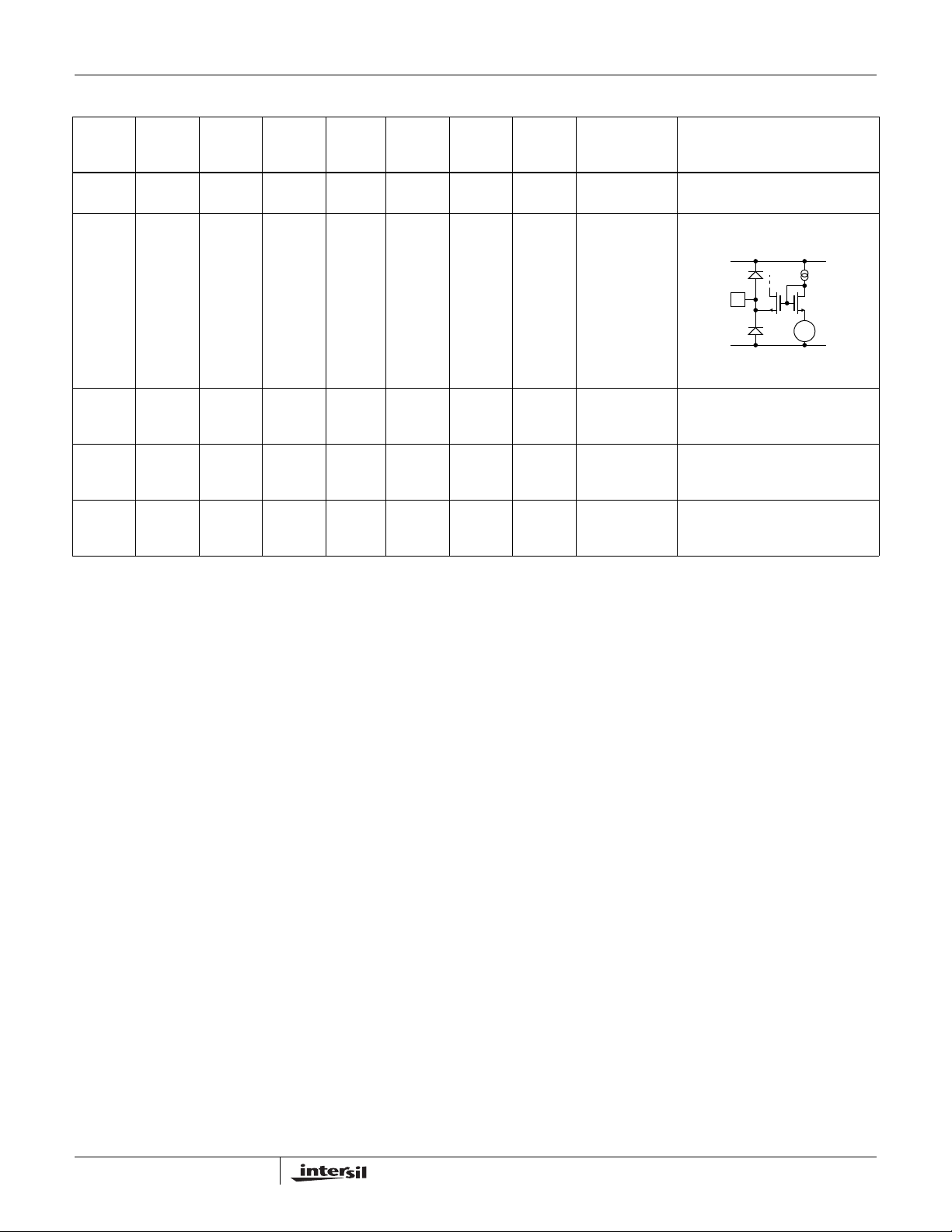
Description of Operation and Applications
Information
Product Description
The EL5144 series is a family of wide bandwidth, single
supply, low power, rail-to-rail output, voltage feedback
operational amplifiers. The family includes single, dual, and
quad configurations. The singles and duals are available with
a power down pin to reduce power to 2.6µA typically. All the
amplifiers are internally compensated for closed loop
feedback gains of +1 or greater . Larger gains are acceptable
but bandwidth will be reduced according to the familiar GainBandwidth Product.
Connected in voltage follower mode and driving a high
impedance load, the EL5144 series has a -3dB bandwidth of
100MHz. Driving a 150Ω load, they have a -3dB bandwidth
of 60MHz while maintaining a 200V/µs slew rate. The input
common mode voltage range includes ground while the
output can swing rail to rail.
Power Supply Bypassing and Printed Circuit
Board Layout
As with any high-frequency device, good printed circuit
board layout is necessary for optimum performance. Ground
plane construction is highly recommended. Lead lengths
should be as short as possible. The power supply pin must
be well bypassed to reduce the risk of oscillation For normal
single supply operation, where the GND pin is connected to
the ground plane, a single 4.7µF tantalum capacitor in
parallel with a 0.1µF ceramic capacitor from V
to GND will
S
suffice. This same capacitor combination should be placed
at each supply pin to ground if split supplies are to be used.
In this case, the GND pin becomes the negative supply rail.
For good AC performance, parasitic capacitance should be
kept to a minimum. Use of wire wound resistors should be
avoided because of their additional series inductance. Use of
sockets, particularly for the SO package, should be avoided
if possible. Sockets add parasitic inductance and
capacitance that can result in compromised performance.
Input, Output, and Supply Voltage Range
The EL5144 series has been designed to operate with a
single supply voltage of 5V. Split supplies can be used so
long as their total range is 5V.
The amplifiers have an input common mode voltage range
that includes the negative supply (GND pin) and extends to
within 1.5V of the positive supply (V
specified over this range.
The output of the EL5144 series amplifiers can swing rail to
rail. As the load resistance becomes lower in value, the
ability to drive close to each rail is reduced. However, even
with an effective 150Ω load resistor connected to a voltage
halfway between the supply rails, the output will swing to
within 150mV of either rail.
pin). They are
S
15

EL5144, EL5146, EL5244, EL5246, EL5444
Figure 1 shows the output of the EL5144 series amplifier
swinging rail to rail with R
Figure 2 is with R
5V
0V
5V
= 150Ω.
L
= 1kΩ, AV = +2 and RL = 1MΩ.
F
FIGURE 1.
Video Performance
For good video signal integrity, an amplifier is required to
maintain the same output impedance and the same
frequency response as DC levels are changed at the output.
This can be difficult when driving a standard video load of
150Ω, because of the change in output current with DC level.
A look at the Differential Gain and Differential Phase curves
for various supply and loading conditions will help you obtain
optimal performance. Curves are provided for A
+2, and R
= 150Ω and 10kΩ tied both to ground as well as
L
2.5V. As with all video amplifiers, there is a common mode
sweet spot for optimum differential gain/differential phase.
For example, with A
= +2 and RL=150Ω tied to 2.5V, and
V
the output common mode voltage kept between 0.8V and
3.2V, dG/dP is a very low 0.1%/0.1°. This condition
corresponds to driving an AC-coupled, double terminated
75Ω coaxial cable. With A
= +1, RL = 150Ω tied to ground,
V
and the video level kept between 0.85V and 2.95V, these
amplifiers provide dG/dP performance of 0.05%/0.20°. This
condition is representative of using the EL5144 series
amplifier as a buffer driving a DC coupled, double
terminated, 75Ω coaxial cable. Driving high impedance
loads, such as signals on computer video cards, gives
similar or better dG/dP performance as driving cables.
= +1 and
V
0V
FIGURE 2.
Choice of Feedback Resistor, R
F
These amplifiers are optimized for applications that require a
gain of +1. Hence, no feedback resistor is required.
However, for gains greater than +1, the feedback resistor
forms a pole with the input capacitance. As this pole
becomes larger, phase margin is reduced. This causes
ringing in the time domain and peaking in the frequency
domain. Therefore, R
has some maximum value that
F
should not be exceeded for optimum performance. If a large
value of R
picofarad range in parallel with R
must be used, a small capacitor in the few
F
can help to reduce this
F
ringing and peaking at the expense of reducing the
bandwidth.
As far as the output stage of the amplifier is concerned, R
R
appear in parallel with RL for gains other than +1. As this
G
+
F
combination gets smaller, the bandwidth falls off.
Consequently, R
also has a minimum value that should not
F
be exceeded for optimum performance.
For A
= +1, RF = 0Ω is optimum. For AV = -1 or +2 (noise
V
gain of 2), optimum response is obtained with R
300Ω and 1kΩ. For A
= -4 or +5 (noise gain of 5), keep R
V
between
F
F
between 300Ω and 15kΩ.
Driving Cables and Capacitive Loads
The EL5144 series amplifiers can drive 50pF loads in
parallel with 150Ω with 4dB of peaking and 100pF with 7dB
of peaking. If less peaking is desired in these applications, a
small series resistor (usually between 5Ω and 50Ω) can be
placed in series with the output to eliminate most peaking.
Howeve r, this will obviously reduce the gain slightly. If your
gain is greater than 1, the gain resistor (R
) can then be
G
chosen to make up for any gain loss which may be created
by this additional resistor at the output. Another method of
reducing peaking is to add a “snubber” circuit at the output. A
snubber is a resistor in a series with a capacitor, 150Ω
and
100pF being typical values. The advantage of a snubber is
that it does not draw DC load current.
When used as a cable driver, double termination is always
recommended for reflection-free performance. For those
applications, the back-termination series resistor will decouple the EL5144 series amplifier from the cable and allow
extensive capacitive drive. However, other applications may
have high capacitive loads without a back-termination
resistor. Again, a small series resistor at the output can
reduce peaking.
Disable/Power-Down
The EL5146 and EL5246 amplifiers can be disabled, placing
its output in a high-impedance state. Turn off time is only
10ns and turn on time is around 500ns. When disabled, the
amplifier’s supply current is reduced to 2.6µA typically,
thereby effectively eliminating power consumption. The
amplifier’s power do wn can be controlled by standard TTL or
CMOS signal levels at the CE pin. The applied logic signal is
16

EL5144, EL5146, EL5244, EL5246, EL5444
relative to the GND pin. Letting the CE pin float will enable
the amplifier. Hence, the 8-pin PDIP and SOIC single amps
are pin compatible with standard amplifiers that don’t have a
power down feature.
Short Circuit Current Limit
The EL5144 series amplifiers do not have internal short
circuit protection circuitry. Short circuit current of 90mA
sourcing and 65mA sinking typically will flow if the output is
trying to drive high or low but is shorted to half way between
the rails. If an output is shorted indefinitely, the power
dissipation could easily increase such that the part will be
destroyed. Maximum reliability is maintained if the output
current never exceeds ±50mA. This limit is set by internal
metal interconnect limitations. Obviously, short circuit
conditions must not remain or the internal metal connections
will be destroyed.
Power Dissipation
With the high output drive capability of the EL5144 series
amplifiers, it is possible to exceed the 150°C Absolute
Maximum junction temperature under certain load current
conditions. Therefore, it is important to calculate the
maximum junction temperature for the application to
determine if load conditions or package type need to be
modified for the amplifier to remain in the safe operating
area.
The maximum power dissipation allowed in a package is
determined according to:
T
- T
PD
MAX
JMAX
---------------------------------------------=
where:
T
= Maximum junction temperature
JMAX
= Maximum ambient temperature
T
AMAX
θ
= Thermal resistance of the package
JA
PD
= Maximum power dissipation in the package
MAX
The maximum power dissipation actually produced by an IC
is the total quiescent supply current times the to tal power
supply voltage, plus the power in the IC due to the load, or:
AMAX
θ
JA
If we set the two PD
can solve for R
--------------------------------------------------------------------------------------------- -=
R
L
:
L
V
OUTVS
- T
T
JMAX
---------------------------------------------
N θJA×
Assuming worst case conditions of T
V
OUT=VS
/2V, VS = 5.5V, and I
below is a table of all packages and the minimum R
equations equal to each other, we
MAX
- V
()×
OUT
AMAX
×()
- V
SISMAX
A
SMAX
= +85°C,
= 8.8mA per amplifier,
L
allowed.
PART PACKAGE MINIMUM R
EL5144CW SOT23-5 37
EL5146CS SOIC-8 21
EL5146CN PDIP-8 14
EL5244CS SOIC-8 48
EL5244CN PDIP-8 30
EL5244CY MSOP-8 69
EL5246CY MSOP-10 69
EL5246CS SOIC-14 34
EL5246CN PDIP-14 23
EL5444CU QSOP-16 139
EL5444CS SOIC-14 85
EL5444CN PDIP-14 51
L
EL5144 Series Comparator Application
The EL5144 series amplifier can be used as a very fast,
single supply comparator. Most op amps used as a
comparator allow only slow speed operation because of
output saturation issues. The EL5144 series amplifier
doesn’t suffer from output saturation issues. Figure 3 shows
the amplifier implemented as a comparator. Figure 4 is a
PD
MAX
NVSI
( - V
SMAXVS
OUT
where:
N = Number of amplifiers in the package
V
= Total supply voltage
S
I
= Maximum supply current per amplifier
SMAX
V
= Maximum output voltage of the application
OUT
RL = Load resistance tied to ground
17
)
×+××=
V
OUT
--------------- -
R
L

EL5144, EL5146, EL5244, EL5246, EL5444
graph of propagation delay vs. overdriv e as a square wav e is
presented at the input of the comparator.
1
EL5146
2
+2.5V
+
V
IN
–
-
+
3
4
FIGURE 3.
Propagation Delay vs. Overdrive for Amplifier
Used as a Comparator
1000
Negative Going Signal
100
Propagation Delay (ns)
Positive Going Signal
10
0.01 0.1 1.0
Overdrive (V)
FIGURE 4.
+5V
8
0.1µF
7
V
6
5
OUT
R
L
directly together. Isolation resistors at each output are not
necessary.
V
1
IN
Select
V
OUT
Select
3V
10MHz
V
2.4V
5MHz
5V
0V
5V
0V
1
PP
-
2
+
3
EL5246
4
5
+
6
2
IN
PP
-
7
14
V
13
12
11
10
9
8
OUT
+5V
0.1µF4.7µF
150Ω
FIGURE 5.
Multiplexing with the EL5144 Series Amplifier
Besides normal power down usage, the CE pin on the
EL5146 and EL5246 series amplifiers also allow for
multiplexing applications. Figure 5 shows an EL5246 with its
outputs tied together, driving a back terminated 75Ω video
load. A 3V
and a 2.4V
shows the SELECT signal that is applied, and the resulting
output waveform at V
operation of the multiplexing. Amp A is on and V
passed through to the output of the amplifier. Then Amp A
turns off in about 10ns. The output decays to ground with an
R
time constants. 500ns later, Amp B turns on and V
LCL
is passed through to the output. This break-before-make
operation ensures that more than one amplifier isn’t trying to
drive the bus at the same time. Notice the outputs are tied
10MHz sine wave is applied at Amp A input,
P-P
5MHz square wave to Amp B. Figure 6
P-P
. Observe the break-befo re -ma ke
OUT
IN1
is being
IN2
FIGURE 6.
Free Running Oscillator Application
Figure 7 is an EL5144 configured as a free running oscillator.
To first order, R
oscillation according to:
F
OSC
---------------------------------------=
R
For rail to rail output swings, maximum frequency of
oscillation is around 15MHz. If reduced output swings are
acceptable, 25MHz can be achieved. Figure 8 shows the
and C
OSC
0.72
×
OSCCOSC
determine the frequency of
OSC
18

EL5144, EL5146, EL5244, EL5246, EL5444
oscillator for R
F
=6MHz.
OSC
V
OUT
OSC
470K
470K
5V
0V
= 510Ω, C
470K
1
+
2
3
FIGURE 7.
= 240pF and
OSC
-
5
4
0.1µF
+5V
R
OSC
C
OSC
FIGURE 8.
5V
0V
FIGURE 9.
All Intersil U.S. products are manufactured, assembled and tested utilizing ISO9000 quality systems.
Intersil Corporation’s quality certifications can be viewed at www.intersil.com/design/quality
Intersil products are sold by description only. Intersil Corporation reserves the right to make changes in circuit design, software and/or specifications at any time without
notice. Accordingly, the reader is cautioned to verify that data sheets are current before placing orders. Information furnished by Intersil is believed to be accurate and
reliable. However, no responsibility is assumed by Intersil or its subsidiaries for its use; nor for any infringements of patents or other rights of third parties which may result
from its use. No license is granted by implication or otherwise under any patent or pat ent rights of In tersi l or its subs idi aries.
For information regarding Intersil Corporation and its products, see www.intersil.com
19
 Loading...